EP1563509B1 - Spin driven resistors and nanogates - Google Patents
Spin driven resistors and nanogates Download PDFInfo
- Publication number
- EP1563509B1 EP1563509B1 EP03774483A EP03774483A EP1563509B1 EP 1563509 B1 EP1563509 B1 EP 1563509B1 EP 03774483 A EP03774483 A EP 03774483A EP 03774483 A EP03774483 A EP 03774483A EP 1563509 B1 EP1563509 B1 EP 1563509B1
- Authority
- EP
- European Patent Office
- Prior art keywords
- spin
- magnetic body
- spin driven
- resistance
- magnetic field
- Prior art date
- Legal status (The legal status is an assumption and is not a legal conclusion. Google has not performed a legal analysis and makes no representation as to the accuracy of the status listed.)
- Expired - Lifetime
Links
Images



Classifications
-
- H—ELECTRICITY
- H01—ELECTRIC ELEMENTS
- H01F—MAGNETS; INDUCTANCES; TRANSFORMERS; SELECTION OF MATERIALS FOR THEIR MAGNETIC PROPERTIES
- H01F10/00—Thin magnetic films, e.g. of one-domain structure
- H01F10/32—Spin-exchange-coupled multilayers, e.g. nanostructured superlattices
- H01F10/3213—Exchange coupling of magnetic semiconductor multilayers, e.g. MnSe/ZnSe superlattices
-
- B—PERFORMING OPERATIONS; TRANSPORTING
- B82—NANOTECHNOLOGY
- B82Y—SPECIFIC USES OR APPLICATIONS OF NANOSTRUCTURES; MEASUREMENT OR ANALYSIS OF NANOSTRUCTURES; MANUFACTURE OR TREATMENT OF NANOSTRUCTURES
- B82Y25/00—Nanomagnetism, e.g. magnetoimpedance, anisotropic magnetoresistance, giant magnetoresistance or tunneling magnetoresistance
-
- G—PHYSICS
- G01—MEASURING; TESTING
- G01R—MEASURING ELECTRIC VARIABLES; MEASURING MAGNETIC VARIABLES
- G01R33/00—Arrangements or instruments for measuring magnetic variables
- G01R33/02—Measuring direction or magnitude of magnetic fields or magnetic flux
- G01R33/06—Measuring direction or magnitude of magnetic fields or magnetic flux using galvano-magnetic devices
-
- G—PHYSICS
- G01—MEASURING; TESTING
- G01R—MEASURING ELECTRIC VARIABLES; MEASURING MAGNETIC VARIABLES
- G01R33/00—Arrangements or instruments for measuring magnetic variables
- G01R33/02—Measuring direction or magnitude of magnetic fields or magnetic flux
- G01R33/06—Measuring direction or magnitude of magnetic fields or magnetic flux using galvano-magnetic devices
- G01R33/09—Magnetoresistive devices
-
- G—PHYSICS
- G11—INFORMATION STORAGE
- G11C—STATIC STORES
- G11C11/00—Digital stores characterised by the use of particular electric or magnetic storage elements; Storage elements therefor
- G11C11/02—Digital stores characterised by the use of particular electric or magnetic storage elements; Storage elements therefor using magnetic elements
- G11C11/16—Digital stores characterised by the use of particular electric or magnetic storage elements; Storage elements therefor using magnetic elements using elements in which the storage effect is based on magnetic spin effect
-
- H—ELECTRICITY
- H01—ELECTRIC ELEMENTS
- H01F—MAGNETS; INDUCTANCES; TRANSFORMERS; SELECTION OF MATERIALS FOR THEIR MAGNETIC PROPERTIES
- H01F10/00—Thin magnetic films, e.g. of one-domain structure
- H01F10/08—Thin magnetic films, e.g. of one-domain structure characterised by magnetic layers
- H01F10/10—Thin magnetic films, e.g. of one-domain structure characterised by magnetic layers characterised by the composition
- H01F10/18—Thin magnetic films, e.g. of one-domain structure characterised by magnetic layers characterised by the composition being compounds
- H01F10/193—Magnetic semiconductor compounds
-
- H—ELECTRICITY
- H01—ELECTRIC ELEMENTS
- H01F—MAGNETS; INDUCTANCES; TRANSFORMERS; SELECTION OF MATERIALS FOR THEIR MAGNETIC PROPERTIES
- H01F10/00—Thin magnetic films, e.g. of one-domain structure
- H01F10/32—Spin-exchange-coupled multilayers, e.g. nanostructured superlattices
- H01F10/324—Exchange coupling of magnetic film pairs via a very thin non-magnetic spacer, e.g. by exchange with conduction electrons of the spacer
-
- Y—GENERAL TAGGING OF NEW TECHNOLOGICAL DEVELOPMENTS; GENERAL TAGGING OF CROSS-SECTIONAL TECHNOLOGIES SPANNING OVER SEVERAL SECTIONS OF THE IPC; TECHNICAL SUBJECTS COVERED BY FORMER USPC CROSS-REFERENCE ART COLLECTIONS [XRACs] AND DIGESTS
- Y10—TECHNICAL SUBJECTS COVERED BY FORMER USPC
- Y10S—TECHNICAL SUBJECTS COVERED BY FORMER USPC CROSS-REFERENCE ART COLLECTIONS [XRACs] AND DIGESTS
- Y10S977/00—Nanotechnology
- Y10S977/902—Specified use of nanostructure
- Y10S977/932—Specified use of nanostructure for electronic or optoelectronic application
Definitions
- This invention relates to spintronic devices. Specifically, this invention relates to spin driven resistors and spin driven nanogates.
- spintronics refers to a new generation of electronic devices that make use of the electron spin as well as its charge. It is anticipated that spintronic devices, such as disclosed in US 2002/0097598 will have superior properties compared to their semiconductor counterparts based on reduced power consumption due to their inherent nonvolatility, elimination of the initial booting-up of random access memory, rapid switching speed, ease of fabrication, and large number of carriers and good thermal conductivity of metals.
- Such devices include giant magnetoresistance (GMR) and tunneling magnetoresistance (TMR) structures that consist of ferromagnetic films separated by metallic or insulating layers, respectively. Switching of the magnetization direction of such elementary units is by means of an external magnetic field that is generated by current pulses in electrical leads that are in proximity.
- the term “resonance” shall mean the process by which the wave amplitude and probability are transferred between two degenerate states, in a manner analogous to the energy transfer between two harmonic oscillators.
- the term “resonance absorption” shall mean the absorption of radiation by an atom (or molecule) at a frequency corresponding to some transition between stationary states.
- the term “resonance frequency” shall mean the frequency at which resonance absorption occurs; the difference between some pair of atomic energy levels divided by Planck's constant.
- One of the goals of the present invention to provide spin driven resistors and nanogates.
- the present invention provides a spin driven resistor system according to the characterising portion of claim 1. Increasing the power of the applied electromagnetic field increases the magnitude of the ratio of change in resistance over resistance. The magnitude of the ratio of change in resistance over resistance decreases with increasing temperatures.
- the magnetic body comprises a material selected from the group of metallic and semi-conducting magnets. It is most preferred that the magnetic body comprise vanadium di-tetracyanoethanide (V[TCNE] 2 ).
- V[TCNE] 2 vanadium di-tetracyanoethanide
- the resistor is held at a constant temperature while being subjected to the externally applied electromagnetic field and/or the externally applied magnetic field.
- the externally applied electromagnetic field comprise microwave radiation. It is most preferred that the microwave radiation have an applied power in the range of about 1 mW to about 25 mW. It is further preferred that the externally applied magnetic field comprise a direct-current (DC) magnetic field.
- DC direct-current
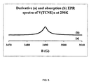
- Figure 5 illustrates derivative (a) and absorption (b) curves for 9.5 GHz EPR of V[TCNE] x at 2.02 mW of applied microwave power at 290K.
- Figure 6 illustrates the ⁇ R/R versus applied magnetic field for applied 9.5 GHz microwave power of 2.02 mW applied to V[TCNE] x films at 290K.
- Figure 7 illustrates the ⁇ R/R versus applied magnetic field for applied 9.5 GHz microwave power of 20.2 mW applied to V[TCNE] x films at 290K.
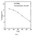
- Figure 8 represents the 20.2 mW ⁇ R/R as a function of temperature from 275K to 298K.
- the present invention includes new types of "spintronic” devices that are termed “spin driven resistor” (SDR) or “spin driven nanogate” (SDN). These devices have potential as a platform technology for information storage and processing as well as in other uses. Examples include magnetic read heads and detectors.
- SDR spin driven resistor
- SDN spin driven nanogate
- a magnetic body was placed in electrical communication with two conducting wires.
- the wires were each connected to a voltage source so as to place a potential across the magnetic body.
- the resistance of the magnetic body was then measured, for example with a voltmeter.
- the magnetic body's resistance was monitored with the voltmeter as the SDR was subjected to an externally applied dc magnetic field.
- a time varying electromagnetic field acted upon the SDR. As the dc magnetic field is increased or decreased so as to pass the value of 'resonance' to occur so electromagnetic energy is absorbed there is a change in the resistance of the sample (increase or decrease), termed the spin driven resistance due to activation of the spin driven nanogate.
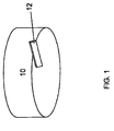
- FIG. 1 is a photograph of a Sum coating of the organic V[TCNE] 2 magnet on a glass cover slide 12 being attracted to a Co 5 Sm magnet 10 at room temperature in air.
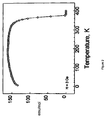
- Figure 2 shows the magnetization (emu/mol) as a function of temperature for the organic V[TCNE] 2 magnet shown in Figure 1 .
- the organic V[TCNE] 2 magnet shows ordering at 370K.
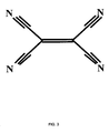
- the chemical structure of tetracyanoethanide is shown in Figure 3 .
- the newly achieved SDR is a spin-dependent quantum effect active at room temperature.
- Figure 4 is a schematic diagram for V[TCNE] 2 showing the half-filled band of TCNE-split into two non-overlapping spin-subbands.
- FIG. 5 shows the 290 K electron paramagnetic resonance (EPR) derivative signal (a) measured for V[TCNE]x films (prepared via low-temperature (40°C) chemical vapor deposition) that are magnetic at room temperature. Also shown in Figure 5 is the absorption curve (b) that represents the power absorbed by the sample. As expected it was found that the EPR line shape and center field depend upon the angle of the V[TCNE]x films with respect to the applied magnetic field.
- EPR electron paramagnetic resonance
- Figures 6 and 7 illustrate the percentage change in resistance at 290 K of the V[TCNE]x film as a function of the applied magnetic field for 2 mW and 20 mW of applied 9.5 GHz microwave power respectively.
- the resistance dramatically increases.
- a ⁇ R/R of 1.3% is achieved for 2 mW of applied microwave power.
- the SDR increases nearly linearly to a ⁇ R/R of 10.5% for applied microwave power of 20 mW as shown in Figure 7 .
- the shape of the ⁇ R/R versus magnetic field curve mimics that of the EPR absorption curve.
- Figure 8 presents the ⁇ R/R as a function of temperature from 275 K to 298 K for a V[TCNE]x film subjected to 20.2 mW of microwave radiation.
- the ⁇ R/R decrease three-fold as the temperature is increased across this temperature range.
- the V[TCNE]x is proposed to be a half semiconductor with a filled lower Hubbard energy band centered on the TCNE-sites (one electron per site).
- x ⁇ 2 typical of samples made, the upper Hubbard band is assumed partly occupied with electrons with spin opposite to that of the electrons in the lower Hubbard band due to the Pauli exclusion principle.
- the conductivity is achieved by electrons hopping among states in the upper Hubbard band.
- spin driven resistors The operation of spin driven resistors is sharply dependent on the applied magnetic field, with the magnetic field for SDR tunable by choice of applied resonance frequency. For example, use of -20 MHz frequency would lead to SDR at ⁇ 7 Oe applied field for the V [TCNE]x based devices.
- SDR may have eventual application in a variety of spintronic devices including read heads and detectors that are very fast and operate at low power.
- the SDR phenomenon may also be used to modulate spin valve, spin tunnel junction, spin-LED, and spin-transistor devices by exposing the magnetic semiconductor or conductor layer to a time varying electromagnetic field and a dc magnetic field so as to pass through a resonance condition.
Landscapes
- Engineering & Computer Science (AREA)
- Chemical & Material Sciences (AREA)
- Physics & Mathematics (AREA)
- Power Engineering (AREA)
- General Physics & Mathematics (AREA)
- Crystallography & Structural Chemistry (AREA)
- Nanotechnology (AREA)
- Condensed Matter Physics & Semiconductors (AREA)
- Materials Engineering (AREA)
- Computer Hardware Design (AREA)
- Hall/Mr Elements (AREA)
- Semiconductor Integrated Circuits (AREA)
- Non-Adjustable Resistors (AREA)
- Measuring Magnetic Variables (AREA)
- Bipolar Transistors (AREA)
- Apparatuses And Processes For Manufacturing Resistors (AREA)
Abstract
Description
- This invention relates to spintronic devices. Specifically, this invention relates to spin driven resistors and spin driven nanogates.
- The term "spintronics" refers to a new generation of electronic devices that make use of the electron spin as well as its charge. It is anticipated that spintronic devices, such as disclosed in
US 2002/0097598 will have superior properties compared to their semiconductor counterparts based on reduced power consumption due to their inherent nonvolatility, elimination of the initial booting-up of random access memory, rapid switching speed, ease of fabrication, and large number of carriers and good thermal conductivity of metals. Such devices include giant magnetoresistance (GMR) and tunneling magnetoresistance (TMR) structures that consist of ferromagnetic films separated by metallic or insulating layers, respectively. Switching of the magnetization direction of such elementary units is by means of an external magnetic field that is generated by current pulses in electrical leads that are in proximity. - As used herein the term "resonance" shall mean the process by which the wave amplitude and probability are transferred between two degenerate states, in a manner analogous to the energy transfer between two harmonic oscillators. As used herein, the term "resonance absorption" shall mean the absorption of radiation by an atom (or molecule) at a frequency corresponding to some transition between stationary states. As used herein, the term "resonance frequency" shall mean the frequency at which resonance absorption occurs; the difference between some pair of atomic energy levels divided by Planck's constant.
- One of the goals of the present invention to provide spin driven resistors and nanogates.
- The present invention provides a spin driven resistor system according to the characterising portion of claim 1. Increasing the power of the applied electromagnetic field increases the magnitude of the ratio of change in resistance over resistance. The magnitude of the ratio of change in resistance over resistance decreases with increasing temperatures.
- Preferably, the magnetic body comprises a material selected from the group of metallic and semi-conducting magnets. It is most preferred that the magnetic body comprise vanadium di-tetracyanoethanide (V[TCNE]2).
- Preferably, the resistor is held at a constant temperature while being subjected to the externally applied electromagnetic field and/or the externally applied magnetic field. It is more preferred that the externally applied electromagnetic field comprise microwave radiation. It is most preferred that the microwave radiation have an applied power in the range of about 1 mW to about 25 mW. It is further preferred that the externally applied magnetic field comprise a direct-current (DC) magnetic field.
-
-
Figure 1 is a photograph of a 5um coating of the organic V[TCNE]2 magnet on a glass cover slide being attracted to a Co5Sm magnet at room temperature in the air. -
Figure 2 shows the magnetization (emu/mol) as a function of temperature showing ordering at 370K for the organic magnet shown inFigure 1 . -
Figure 3 illustrates the chemical structure of tetracyanoethanide. -
Figure 4 is a schematic level diagram for V[TCNE]2 showing the half-filled π*-band of TCNE' split into two non-overlapping spin-subbands. -
Figure 5 illustrates derivative (a) and absorption (b) curves for 9.5 GHz EPR of V[TCNE]x at 2.02 mW of applied microwave power at 290K. -
Figure 6 illustrates the ΔR/R versus applied magnetic field for applied 9.5 GHz microwave power of 2.02 mW applied to V[TCNE]x films at 290K. -
Figure 7 illustrates the ΔR/R versus applied magnetic field for applied 9.5 GHz microwave power of 20.2 mW applied to V[TCNE]x films at 290K. -
Figure 8 represents the 20.2 mW ΔR/R as a function of temperature from 275K to 298K. - The present invention includes new types of "spintronic" devices that are termed "spin driven resistor" (SDR) or "spin driven nanogate" (SDN). These devices have potential as a platform technology for information storage and processing as well as in other uses. Examples include magnetic read heads and detectors.
- In developing the spin driven resistor (SDR) of the present invention, a magnetic body was placed in electrical communication with two conducting wires. The wires were each connected to a voltage source so as to place a potential across the magnetic body. The resistance of the magnetic body was then measured, for example with a voltmeter. The magnetic body's resistance was monitored with the voltmeter as the SDR was subjected to an externally applied dc magnetic field. Additionally, a time varying electromagnetic field acted upon the SDR. As the dc magnetic field is increased or decreased so as to pass the value of 'resonance' to occur so electromagnetic energy is absorbed there is a change in the resistance of the sample (increase or decrease), termed the spin driven resistance due to activation of the spin driven nanogate.
- Metallic or semiconducting magnets with a substantial excess of one polarization of conduction carrier spin polarization over the opposite of spin polarization are preferred.
- A spin driven resistor of the present invention was developed using the "half-semiconductor" V[TCNE]x.
Figure 1 is a photograph of a Sum coating of the organic V[TCNE]2 magnet on aglass cover slide 12 being attracted to a Co5Sm magnet 10 at room temperature in air.Figure 2 shows the magnetization (emu/mol) as a function of temperature for the organic V[TCNE]2 magnet shown inFigure 1 . As can be seen fromFigure 2 , the organic V[TCNE]2 magnet shows ordering at 370K. The chemical structure of tetracyanoethanide is shown inFigure 3 . The newly achieved SDR is a spin-dependent quantum effect active at room temperature. -
Figure 4 is a schematic diagram for V[TCNE]2 showing the half-filled band of TCNE-split into two non-overlapping spin-subbands. -
Figure 5 shows the 290 K electron paramagnetic resonance (EPR) derivative signal (a) measured for V[TCNE]x films (prepared via low-temperature (40°C) chemical vapor deposition) that are magnetic at room temperature. Also shown inFigure 5 is the absorption curve (b) that represents the power absorbed by the sample. As expected it was found that the EPR line shape and center field depend upon the angle of the V[TCNE]x films with respect to the applied magnetic field. -
Figures 6 and7 illustrate the percentage change in resistance at 290 K of the V[TCNE]x film as a function of the applied magnetic field for 2 mW and 20 mW of applied 9.5 GHz microwave power respectively. As the magnetic field sweeps past the field for resonance (3492 Oersted), the resistance dramatically increases. As seen inFigure 6 , a ΔR/R of 1.3% is achieved for 2 mW of applied microwave power. The SDR increases nearly linearly to a ΔR/R of 10.5% for applied microwave power of 20 mW as shown inFigure 7 . The shape of the ΔR/R versus magnetic field curve mimics that of the EPR absorption curve. -
Figure 8 presents the ΔR/R as a function of temperature from 275 K to 298 K for a V[TCNE]x film subjected to 20.2 mW of microwave radiation. The ΔR/R decrease three-fold as the temperature is increased across this temperature range. - A proposed mechanism for spin driven resistor operation may be understood by viewing
Figure 4 . The V[TCNE]x is proposed to be a half semiconductor with a filled lower Hubbard energy band centered on the TCNE-sites (one electron per site). The magnetic exchange coupling of the spin S =1/2 of TCNE-sites with the S = 3/2 of V2+ sites result in all of the sites in this lower Hubbard band being in the same spin direction. With x < 2, typical of samples made, the upper Hubbard band is assumed partly occupied with electrons with spin opposite to that of the electrons in the lower Hubbard band due to the Pauli exclusion principle. The conductivity is achieved by electrons hopping among states in the upper Hubbard band. - It is further believed that at resonance, the applied microwave field flips some of the spins in the lower Hubbard band of localized states.
- These 'inverted' states then block passage of the spin (and associated charge) in the upper Hubbard band thereby increasing the resistance. In essence, each TCNE-becomes a "spin-driven nanogate". At finite temperatures some thermally reversed spins already exist. By lowering the temperature, the ratio of minority to majority spin sites decreases making the effect of spin flip due to resonant microwave field larger, in agreement with
Figure 8 . - The operation of spin driven resistors is sharply dependent on the applied magnetic field, with the magnetic field for SDR tunable by choice of applied resonance frequency. For example, use of -20 MHz frequency would lead to SDR at ~7 Oe applied field for the V [TCNE]x based devices.
- It is noted that SDR may have eventual application in a variety of spintronic devices including read heads and detectors that are very fast and operate at low power. The SDR phenomenon may also be used to modulate spin valve, spin tunnel junction, spin-LED, and spin-transistor devices by exposing the magnetic semiconductor or conductor layer to a time varying electromagnetic field and a dc magnetic field so as to pass through a resonance condition.
Claims (8)
- A spin driven resistor system comprising:a voltage source;a magnetic body being subjected to an externally - applied magnetic field, said magnetic body having a resonance frequency and being electrically connected to the voltage source so as to, in use, place a potential across the magnetic body;the magnetic body having a resistance to said potential imposed thereacross, the resistance increasing from a base resistance as the power of the externally-applied magnetic field increases;characterized by:an electromagnetic field source arranged to apply a time-varying externally-applied electromagnetic field to said magnetic body at said resonance frequency of the magnetic body so as to maximize a ratio of the increased resistance to the base resistance.
- The spin driven resistor system according to claim 1 wherein the magnetic body comprises a material selected from the group consisting of metallic and semi-conducting magnets.
- The spin driven resistor system according to claim 1 wherein the magnetic body comprises vanadium di-tetracyanoethanide.
- The spin driven resistor system according to claim 1 wherein the spin driven resistor is held at a constant temperature.
- The spin driven resistor system according to claim 1 further comprising a magnetic field source arranged to apply a direct-current magnetic field to said magnetic body.
- The spin driven resistor system according to claim 1 wherein the externally applied electromagnetic field comprises microwave radiation.
- The spin driven resistor system according to claim 6 wherein the microwave radiation has a power in the range of about 1 mW to about 25 mW.
- The spin driven resistance system according to claim 1 wherein the maximum ratio of the increased resistance to the base resistance decreases as temperature increases.
Applications Claiming Priority (3)
| Application Number | Priority Date | Filing Date | Title |
|---|---|---|---|
| US41192302P | 2002-09-19 | 2002-09-19 | |
| US411923P | 2002-09-19 | ||
| PCT/US2003/029664 WO2004028002A2 (en) | 2002-09-19 | 2003-09-19 | Spin driven resistors and nanogates |
Publications (3)
| Publication Number | Publication Date |
|---|---|
| EP1563509A2 EP1563509A2 (en) | 2005-08-17 |
| EP1563509A4 EP1563509A4 (en) | 2006-03-08 |
| EP1563509B1 true EP1563509B1 (en) | 2011-03-09 |
Family
ID=32030763
Family Applications (1)
| Application Number | Title | Priority Date | Filing Date |
|---|---|---|---|
| EP03774483A Expired - Lifetime EP1563509B1 (en) | 2002-09-19 | 2003-09-19 | Spin driven resistors and nanogates |
Country Status (7)
| Country | Link |
|---|---|
| US (1) | US7075815B2 (en) |
| EP (1) | EP1563509B1 (en) |
| JP (1) | JP5060022B2 (en) |
| AT (1) | ATE501512T1 (en) |
| AU (1) | AU2003282805A1 (en) |
| DE (1) | DE60336337D1 (en) |
| WO (1) | WO2004028002A2 (en) |
Families Citing this family (6)
| Publication number | Priority date | Publication date | Assignee | Title |
|---|---|---|---|---|
| US7099122B2 (en) * | 2003-12-16 | 2006-08-29 | Seagate Technology Llc | Spin polarization enhancement artificial magnet |
| US8326389B2 (en) * | 2006-12-07 | 2012-12-04 | The Ohio State University Research Foundation | System for in vivo biosensing based on the optical response of electronic polymers |
| US8941379B2 (en) | 2009-05-14 | 2015-01-27 | University Of Delaware | Electromagnetic wave detection systems and methods |
| WO2010132541A2 (en) | 2009-05-14 | 2010-11-18 | University Of Delaware | Electromagnetic detection apparatus and methods |
| US8808861B2 (en) | 2010-11-18 | 2014-08-19 | The Ohio State University | Laminate composite and method for making same |
| CN113176483B (en) * | 2020-01-09 | 2023-04-28 | 国家纳米科学中心 | Spin signal measurement method and system for spin field effect transistor |
Family Cites Families (10)
| Publication number | Priority date | Publication date | Assignee | Title |
|---|---|---|---|---|
| JP2569542B2 (en) * | 1987-03-28 | 1997-01-08 | 株式会社日立製作所 | Magnetic flux transmission circuit |
| JPH07193184A (en) * | 1993-12-27 | 1995-07-28 | Fujitsu Ltd | Manufacturing method of multi-chip module and multi-chip module |
| JP2000040212A (en) * | 1998-07-24 | 2000-02-08 | Alps Electric Co Ltd | Spin valve type thin film element |
| US6172902B1 (en) * | 1998-08-12 | 2001-01-09 | Ecole Polytechnique Federale De Lausanne (Epfl) | Non-volatile magnetic random access memory |
| US6381171B1 (en) * | 1999-05-19 | 2002-04-30 | Kabushiki Kaisha Toshiba | Magnetic element, magnetic read head, magnetic storage device, magnetic memory device |
| US6249453B1 (en) * | 2000-04-18 | 2001-06-19 | The University Of Chicago | Voltage controlled spintronic devices for logic applications |
| FR2813987B1 (en) * | 2000-09-12 | 2003-01-10 | Memscap | MICRO-COMPONENT OF THE MICRO-INDUCTANCE OR MICRO-TRANSFORMER TYPE |
| US6490194B2 (en) * | 2001-01-24 | 2002-12-03 | Infineon Technologies Ag | Serial MRAM device |
| US6864418B2 (en) * | 2002-12-18 | 2005-03-08 | Nanoset, Llc | Nanomagnetically shielded substrate |
| US6753562B1 (en) * | 2003-03-27 | 2004-06-22 | Sharp Laboratories Of America, Inc. | Spin transistor magnetic random access memory device |
-
2003
- 2003-09-19 EP EP03774483A patent/EP1563509B1/en not_active Expired - Lifetime
- 2003-09-19 US US10/665,253 patent/US7075815B2/en not_active Expired - Fee Related
- 2003-09-19 WO PCT/US2003/029664 patent/WO2004028002A2/en not_active Ceased
- 2003-09-19 JP JP2004538322A patent/JP5060022B2/en not_active Expired - Fee Related
- 2003-09-19 AU AU2003282805A patent/AU2003282805A1/en not_active Abandoned
- 2003-09-19 DE DE60336337T patent/DE60336337D1/en not_active Expired - Lifetime
- 2003-09-19 AT AT03774483T patent/ATE501512T1/en not_active IP Right Cessation
Also Published As
| Publication number | Publication date |
|---|---|
| JP2006500770A (en) | 2006-01-05 |
| DE60336337D1 (en) | 2011-04-21 |
| ATE501512T1 (en) | 2011-03-15 |
| US7075815B2 (en) | 2006-07-11 |
| JP5060022B2 (en) | 2012-10-31 |
| US20040109350A1 (en) | 2004-06-10 |
| AU2003282805A8 (en) | 2004-04-08 |
| WO2004028002A2 (en) | 2004-04-01 |
| EP1563509A4 (en) | 2006-03-08 |
| WO2004028002A3 (en) | 2005-06-16 |
| EP1563509A2 (en) | 2005-08-17 |
| AU2003282805A1 (en) | 2004-04-08 |
Similar Documents
| Publication | Publication Date | Title |
|---|---|---|
| Kao | Dielectric phenomena in solids | |
| Walter et al. | Voltage-induced ferromagnetism in a diamagnet | |
| US8254163B2 (en) | Spintronic device and information transmitting method | |
| US11422209B2 (en) | Magnetic tunnel barriers and related heterostructure devices and methods | |
| KR20180136556A (en) | Magnetic tunnel junction | |
| JP2005501404A (en) | Magnetoresistive device and electronic device | |
| WO2009152434A2 (en) | Method and apparatus for measuring magnetic fields | |
| Raju et al. | Anomalous magnetoresistance in high-temperature organic-based magnetic semiconducting V (TCNE) x films | |
| Kim et al. | Electrical detection of the surface spin polarization of the candidate topological Kondo insulator Sm B 6 | |
| Healey et al. | Varied magnetic phases in a van der Waals easy-plane antiferromagnet revealed by nitrogen-vacancy center microscopy | |
| Burger et al. | Atomic force manipulation of single magnetic nanoparticles for spin-based electronics | |
| US7075815B2 (en) | Spin driven resistors and nanogates | |
| KR102235692B1 (en) | Low-Power Terahertz Magnetic Nano-oscillators | |
| Zhang et al. | Magnetic-field-controlled spin valve and spin memory based on single-molecule magnets | |
| Negishi et al. | Dielectric ordering and colossal magnetodielectricity in the antiferromagnetic insulating state of λ-(BEDT-TSF) 2 Fe Cl 4 | |
| Tao et al. | Magnetization Switching by Spin–Orbit Torque in L1 0-FePt and Ta/FePt Films With Large Perpendicular Magnetic Anisotropy | |
| ES3001458T3 (en) | A magnetoelectric device and uses of the magnetoelectric device | |
| US20150072442A1 (en) | Spin injector device comprising a protection layer at the centre thereof | |
| JP3240310B2 (en) | Magnetoresistance effect element | |
| JP2005503034A (en) | Bias field compensation in the memory layer of magnetoresistive memory cells. | |
| Jacobsen et al. | Organic conductors: Electrical and magnetic properties of tetrathiafulvalenium-methyl-tetracyano-p-quinodimethanide (TTF-MTCNQ) | |
| Zhang | Anomalous Metals and Quantum Superconductor-Metal-Insulator Transitions in Two-Dimensional Granular Superconductors | |
| Bodepudi | Design and construction of ultrahigh vacuum system to fabricateSpintronic devices, fabrication and characterization of OMAR (organic magnetoresistance) devices | |
| Zadvorna | Spin pumping measurements at interfaces between magnetic metal or insulator and organic semiconductors | |
| BĂJENESCU | Challenges of Spintronics. |
Legal Events
| Date | Code | Title | Description |
|---|---|---|---|
| PUAI | Public reference made under article 153(3) epc to a published international application that has entered the european phase |
Free format text: ORIGINAL CODE: 0009012 |
|
| AK | Designated contracting states |
Kind code of ref document: A2 Designated state(s): AT BE BG CH CY CZ DE DK EE ES FI FR GB GR HU IE IT LI LU MC NL PT RO SE SI SK TR |
|
| AX | Request for extension of the european patent |
Extension state: AL LT LV MK |
|
| DAX | Request for extension of the european patent (deleted) | ||
| 17P | Request for examination filed |
Effective date: 20051216 |
|
| RBV | Designated contracting states (corrected) |
Designated state(s): AT BE BG CH CY CZ DE DK EE ES FI FR GB GR HU IE IT LI LU MC NL PT RO SE SI SK TR |
|
| A4 | Supplementary search report drawn up and despatched |
Effective date: 20060119 |
|
| RIC1 | Information provided on ipc code assigned before grant |
Ipc: G11C 11/16 20060101AFI20060113BHEP Ipc: G01R 33/09 20060101ALI20060113BHEP |
|
| GRAP | Despatch of communication of intention to grant a patent |
Free format text: ORIGINAL CODE: EPIDOSNIGR1 |
|
| GRAS | Grant fee paid |
Free format text: ORIGINAL CODE: EPIDOSNIGR3 |
|
| GRAA | (expected) grant |
Free format text: ORIGINAL CODE: 0009210 |
|
| AK | Designated contracting states |
Kind code of ref document: B1 Designated state(s): AT BE BG CH CY CZ DE DK EE ES FI FR GB GR HU IE IT LI LU MC NL PT RO SE SI SK TR |
|
| REG | Reference to a national code |
Ref country code: GB Ref legal event code: FG4D |
|
| REG | Reference to a national code |
Ref country code: CH Ref legal event code: EP |
|
| REG | Reference to a national code |
Ref country code: IE Ref legal event code: FG4D |
|
| REF | Corresponds to: |
Ref document number: 60336337 Country of ref document: DE Date of ref document: 20110421 Kind code of ref document: P |
|
| REG | Reference to a national code |
Ref country code: DE Ref legal event code: R096 Ref document number: 60336337 Country of ref document: DE Effective date: 20110421 |
|
| REG | Reference to a national code |
Ref country code: SE Ref legal event code: TRGR |
|
| REG | Reference to a national code |
Ref country code: NL Ref legal event code: VDEP Effective date: 20110309 |
|
| PG25 | Lapsed in a contracting state [announced via postgrant information from national office to epo] |
Ref country code: GR Free format text: LAPSE BECAUSE OF FAILURE TO SUBMIT A TRANSLATION OF THE DESCRIPTION OR TO PAY THE FEE WITHIN THE PRESCRIBED TIME-LIMIT Effective date: 20110610 Ref country code: ES Free format text: LAPSE BECAUSE OF FAILURE TO SUBMIT A TRANSLATION OF THE DESCRIPTION OR TO PAY THE FEE WITHIN THE PRESCRIBED TIME-LIMIT Effective date: 20110620 |
|
| PG25 | Lapsed in a contracting state [announced via postgrant information from national office to epo] |
Ref country code: NL Free format text: LAPSE BECAUSE OF FAILURE TO SUBMIT A TRANSLATION OF THE DESCRIPTION OR TO PAY THE FEE WITHIN THE PRESCRIBED TIME-LIMIT Effective date: 20110309 Ref country code: FI Free format text: LAPSE BECAUSE OF FAILURE TO SUBMIT A TRANSLATION OF THE DESCRIPTION OR TO PAY THE FEE WITHIN THE PRESCRIBED TIME-LIMIT Effective date: 20110309 Ref country code: BG Free format text: LAPSE BECAUSE OF FAILURE TO SUBMIT A TRANSLATION OF THE DESCRIPTION OR TO PAY THE FEE WITHIN THE PRESCRIBED TIME-LIMIT Effective date: 20110609 Ref country code: AT Free format text: LAPSE BECAUSE OF FAILURE TO SUBMIT A TRANSLATION OF THE DESCRIPTION OR TO PAY THE FEE WITHIN THE PRESCRIBED TIME-LIMIT Effective date: 20110309 Ref country code: SI Free format text: LAPSE BECAUSE OF FAILURE TO SUBMIT A TRANSLATION OF THE DESCRIPTION OR TO PAY THE FEE WITHIN THE PRESCRIBED TIME-LIMIT Effective date: 20110309 Ref country code: CY Free format text: LAPSE BECAUSE OF FAILURE TO SUBMIT A TRANSLATION OF THE DESCRIPTION OR TO PAY THE FEE WITHIN THE PRESCRIBED TIME-LIMIT Effective date: 20110309 |
|
| PG25 | Lapsed in a contracting state [announced via postgrant information from national office to epo] |
Ref country code: BE Free format text: LAPSE BECAUSE OF FAILURE TO SUBMIT A TRANSLATION OF THE DESCRIPTION OR TO PAY THE FEE WITHIN THE PRESCRIBED TIME-LIMIT Effective date: 20110309 |
|
| PG25 | Lapsed in a contracting state [announced via postgrant information from national office to epo] |
Ref country code: EE Free format text: LAPSE BECAUSE OF FAILURE TO SUBMIT A TRANSLATION OF THE DESCRIPTION OR TO PAY THE FEE WITHIN THE PRESCRIBED TIME-LIMIT Effective date: 20110309 Ref country code: PT Free format text: LAPSE BECAUSE OF FAILURE TO SUBMIT A TRANSLATION OF THE DESCRIPTION OR TO PAY THE FEE WITHIN THE PRESCRIBED TIME-LIMIT Effective date: 20110711 |
|
| PG25 | Lapsed in a contracting state [announced via postgrant information from national office to epo] |
Ref country code: CZ Free format text: LAPSE BECAUSE OF FAILURE TO SUBMIT A TRANSLATION OF THE DESCRIPTION OR TO PAY THE FEE WITHIN THE PRESCRIBED TIME-LIMIT Effective date: 20110309 Ref country code: SK Free format text: LAPSE BECAUSE OF FAILURE TO SUBMIT A TRANSLATION OF THE DESCRIPTION OR TO PAY THE FEE WITHIN THE PRESCRIBED TIME-LIMIT Effective date: 20110309 Ref country code: RO Free format text: LAPSE BECAUSE OF FAILURE TO SUBMIT A TRANSLATION OF THE DESCRIPTION OR TO PAY THE FEE WITHIN THE PRESCRIBED TIME-LIMIT Effective date: 20110309 |
|
| PLBE | No opposition filed within time limit |
Free format text: ORIGINAL CODE: 0009261 |
|
| STAA | Information on the status of an ep patent application or granted ep patent |
Free format text: STATUS: NO OPPOSITION FILED WITHIN TIME LIMIT |
|
| 26N | No opposition filed |
Effective date: 20111212 |
|
| PG25 | Lapsed in a contracting state [announced via postgrant information from national office to epo] |
Ref country code: DK Free format text: LAPSE BECAUSE OF FAILURE TO SUBMIT A TRANSLATION OF THE DESCRIPTION OR TO PAY THE FEE WITHIN THE PRESCRIBED TIME-LIMIT Effective date: 20110309 |
|
| REG | Reference to a national code |
Ref country code: DE Ref legal event code: R097 Ref document number: 60336337 Country of ref document: DE Effective date: 20111212 |
|
| PG25 | Lapsed in a contracting state [announced via postgrant information from national office to epo] |
Ref country code: MC Free format text: LAPSE BECAUSE OF NON-PAYMENT OF DUE FEES Effective date: 20110930 |
|
| REG | Reference to a national code |
Ref country code: CH Ref legal event code: PL |
|
| GBPC | Gb: european patent ceased through non-payment of renewal fee |
Effective date: 20110919 |
|
| PG25 | Lapsed in a contracting state [announced via postgrant information from national office to epo] |
Ref country code: IT Free format text: LAPSE BECAUSE OF FAILURE TO SUBMIT A TRANSLATION OF THE DESCRIPTION OR TO PAY THE FEE WITHIN THE PRESCRIBED TIME-LIMIT Effective date: 20110309 |
|
| REG | Reference to a national code |
Ref country code: IE Ref legal event code: MM4A |
|
| REG | Reference to a national code |
Ref country code: DE Ref legal event code: R119 Ref document number: 60336337 Country of ref document: DE Effective date: 20120403 |
|
| PG25 | Lapsed in a contracting state [announced via postgrant information from national office to epo] |
Ref country code: DE Free format text: LAPSE BECAUSE OF NON-PAYMENT OF DUE FEES Effective date: 20120403 Ref country code: CH Free format text: LAPSE BECAUSE OF NON-PAYMENT OF DUE FEES Effective date: 20110930 Ref country code: IE Free format text: LAPSE BECAUSE OF NON-PAYMENT OF DUE FEES Effective date: 20110919 Ref country code: LI Free format text: LAPSE BECAUSE OF NON-PAYMENT OF DUE FEES Effective date: 20110930 |
|
| PG25 | Lapsed in a contracting state [announced via postgrant information from national office to epo] |
Ref country code: GB Free format text: LAPSE BECAUSE OF NON-PAYMENT OF DUE FEES Effective date: 20110919 |
|
| PG25 | Lapsed in a contracting state [announced via postgrant information from national office to epo] |
Ref country code: LU Free format text: LAPSE BECAUSE OF NON-PAYMENT OF DUE FEES Effective date: 20110919 |
|
| PG25 | Lapsed in a contracting state [announced via postgrant information from national office to epo] |
Ref country code: TR Free format text: LAPSE BECAUSE OF FAILURE TO SUBMIT A TRANSLATION OF THE DESCRIPTION OR TO PAY THE FEE WITHIN THE PRESCRIBED TIME-LIMIT Effective date: 20110309 |
|
| PG25 | Lapsed in a contracting state [announced via postgrant information from national office to epo] |
Ref country code: HU Free format text: LAPSE BECAUSE OF FAILURE TO SUBMIT A TRANSLATION OF THE DESCRIPTION OR TO PAY THE FEE WITHIN THE PRESCRIBED TIME-LIMIT Effective date: 20110309 |
|
| PGFP | Annual fee paid to national office [announced via postgrant information from national office to epo] |
Ref country code: FR Payment date: 20140917 Year of fee payment: 12 Ref country code: SE Payment date: 20140929 Year of fee payment: 12 |
|
| REG | Reference to a national code |
Ref country code: SE Ref legal event code: EUG |
|
| PG25 | Lapsed in a contracting state [announced via postgrant information from national office to epo] |
Ref country code: SE Free format text: LAPSE BECAUSE OF NON-PAYMENT OF DUE FEES Effective date: 20150920 |
|
| REG | Reference to a national code |
Ref country code: FR Ref legal event code: ST Effective date: 20160531 |
|
| PG25 | Lapsed in a contracting state [announced via postgrant information from national office to epo] |
Ref country code: FR Free format text: LAPSE BECAUSE OF NON-PAYMENT OF DUE FEES Effective date: 20150930 |