EP1563500B1 - An efficient analog front end for a read/write channel of a hard disk drive running from a highly regulated power supply - Google Patents
An efficient analog front end for a read/write channel of a hard disk drive running from a highly regulated power supply Download PDFInfo
- Publication number
- EP1563500B1 EP1563500B1 EP02808174.3A EP02808174A EP1563500B1 EP 1563500 B1 EP1563500 B1 EP 1563500B1 EP 02808174 A EP02808174 A EP 02808174A EP 1563500 B1 EP1563500 B1 EP 1563500B1
- Authority
- EP
- European Patent Office
- Prior art keywords
- voltage
- read
- write channel
- write
- power supply
- Prior art date
- Legal status (The legal status is an assumption and is not a legal conclusion. Google has not performed a legal analysis and makes no representation as to the accuracy of the status listed.)
- Expired - Lifetime
Links
- 230000001105 regulatory effect Effects 0.000 title claims description 24
- 238000000034 method Methods 0.000 claims description 28
- 239000000872 buffer Substances 0.000 claims description 14
- 230000008569 process Effects 0.000 claims description 11
- 238000012360 testing method Methods 0.000 claims description 7
- 238000012545 processing Methods 0.000 claims description 4
- 229920005994 diacetyl cellulose Polymers 0.000 description 21
- 230000004907 flux Effects 0.000 description 12
- 238000005516 engineering process Methods 0.000 description 8
- 238000004519 manufacturing process Methods 0.000 description 6
- 238000001514 detection method Methods 0.000 description 5
- 238000010586 diagram Methods 0.000 description 5
- 230000004044 response Effects 0.000 description 4
- 238000004088 simulation Methods 0.000 description 4
- 238000012795 verification Methods 0.000 description 4
- 238000007476 Maximum Likelihood Methods 0.000 description 3
- 238000012937 correction Methods 0.000 description 3
- 238000013461 design Methods 0.000 description 3
- 230000036961 partial effect Effects 0.000 description 3
- 238000004891 communication Methods 0.000 description 2
- 238000013500 data storage Methods 0.000 description 2
- 230000003247 decreasing effect Effects 0.000 description 2
- 238000011084 recovery Methods 0.000 description 2
- 230000002829 reductive effect Effects 0.000 description 2
- 238000012546 transfer Methods 0.000 description 2
- XUIMIQQOPSSXEZ-UHFFFAOYSA-N Silicon Chemical compound [Si] XUIMIQQOPSSXEZ-UHFFFAOYSA-N 0.000 description 1
- 230000002238 attenuated effect Effects 0.000 description 1
- 239000003990 capacitor Substances 0.000 description 1
- 230000008859 change Effects 0.000 description 1
- 238000006243 chemical reaction Methods 0.000 description 1
- 230000000295 complement effect Effects 0.000 description 1
- 230000005672 electromagnetic field Effects 0.000 description 1
- 230000000670 limiting effect Effects 0.000 description 1
- 239000002184 metal Substances 0.000 description 1
- 229910044991 metal oxide Inorganic materials 0.000 description 1
- 150000004706 metal oxides Chemical class 0.000 description 1
- 238000012986 modification Methods 0.000 description 1
- 230000004048 modification Effects 0.000 description 1
- 229910021420 polycrystalline silicon Inorganic materials 0.000 description 1
- 229920005591 polysilicon Polymers 0.000 description 1
- 230000035755 proliferation Effects 0.000 description 1
- 239000004065 semiconductor Substances 0.000 description 1
- 230000035945 sensitivity Effects 0.000 description 1
- 229910052710 silicon Inorganic materials 0.000 description 1
- 239000010703 silicon Substances 0.000 description 1
Images


Classifications
-
- G—PHYSICS
- G11—INFORMATION STORAGE
- G11B—INFORMATION STORAGE BASED ON RELATIVE MOVEMENT BETWEEN RECORD CARRIER AND TRANSDUCER
- G11B20/00—Signal processing not specific to the method of recording or reproducing; Circuits therefor
- G11B20/10—Digital recording or reproducing
- G11B20/10009—Improvement or modification of read or write signals
-
- G—PHYSICS
- G11—INFORMATION STORAGE
- G11B—INFORMATION STORAGE BASED ON RELATIVE MOVEMENT BETWEEN RECORD CARRIER AND TRANSDUCER
- G11B20/00—Signal processing not specific to the method of recording or reproducing; Circuits therefor
- G11B20/10—Digital recording or reproducing
- G11B20/14—Digital recording or reproducing using self-clocking codes
- G11B20/1403—Digital recording or reproducing using self-clocking codes characterised by the use of two levels
Definitions
- Computer hard disk drives also known as fixed disk drives or hard drives, have become a de facto standard data storage component of modem computer systems and are making further inroads into modem consumer electronics as well. Their proliferation can be directly attributed to their low cost, high storage capacity and high reliability, in addition to wide availability, low power consumption, high data transfer speeds and decreasing physical size.
- These disk drives typically consist of one or more rotating magnetic platters encased within an environmentally controlled housing that further includes all of the electronics and mechanics to read and write data and interface with other devices.
- Read/write heads are positioned above each of the platters, and typically on each face, to record and read data.
- the electronics of a hard disk drive are coupled with these read/write heads and include numerous components to control the position of the heads and generate or sense the electromagnetic fields representing data. These components receive data from a host device, such as a personal computer, and translate that data into magnetic encodings written onto the disk platters by the heads.
- the electronics locate the desired data, sense the magnetic encodings which represent that data and translate those encodings back into the binary digital information which the host device can understand. Further, error detection and correction algorithms are applied to ensure accurate storage and retrieval of data.
- the read/write head of which a typical hard disk has several, is the interface between magnetic platters and the disk drive electronics.
- the read/write head actually reads and writes the magnetically encoded data as areas of magnetic flux on the platters.
- Data consisting of binary 1's and 0's, are encoded by sequences of the presence or absence of flux reversals recorded or detected by the read/write head.
- a flux reversal is a change in the magnetic flux in two contiguous areas of the disk platter.
- PRML Partial Response Maximum Likelihood
- PRML-based drives digitally sample this analog waveform (the "Partial Response") and use advanced signal processing technologies to determine the bit pattern represented by that wave form (the “Maximum Likelihood”).
- This technology in conjunction magneto-resistive (“MR”) heads, have permitted manufacturers to further increase data storage densities. PRML technology further tolerates more noise in the sensed magnetic signals permitting the use of lower quality platters and read/write heads which increases manufacturing yields and lowers costs.
- the read/write heads of the hard disk drive are coupled with a device called a read/write channel.
- the phrase "coupled with” is defined to mean directly connected to or indirectly connected with through one or more intermediate components.
- Such intermediate components may include both hardware and software based components.
- the read/write channel converts binary/digital data from the host device into the electrical impulses which drive the read/write head to magnetically record the data to the disk drive platters. Further, the read/write channel receives the analog waveform magnetically sensed by the read/write heads and converts that waveform back into the binary/digital data stored on the drive.
- hard disk drives are typically differentiated by factors such as cost/megabyte of storage, data transfer rate, power requirements and form factor (physical dimensions) with the bulk of competition based on cost.
- factors such as cost/megabyte of storage, data transfer rate, power requirements and form factor (physical dimensions) with the bulk of competition based on cost.
- the read/write channel of the hard drive typically includes an analog portion, which is used to convert digital signals received from a controller to analog signals which then get sent to the read/write heads.
- the analog portion may also be used to receive analog signals from the read/write heads and convert them into digital signals.
- the analog portion of the read/write channel 108 is manufactured using one of two methods.
- the first method is to use only high voltage transistors which all operate within the same voltage range. However, high voltage transistors require a lot of power, are relatively slow, and do not scale so well with a CMOS manufacturing process.
- the second method is to use both high voltage transistors and low voltage transistors and use a power supply voltage, which is substantially higher than the maximum rating for the low voltage transistors.
- Low voltage transistors operate at a higher speed, occupy less silicon area, and consume less power than high voltage transistors.
- low voltage transistors are used in a core area of a circuit and high voltage transistors are used in an I/O area of the circuit.
- the analog portion may include high voltage transistors that operate at a voltage range of between 2.16 volts and 2.64 volts (2.4 volts +/- 10%), and low voltage transistors that operate at a lower voltage range, such as between 1.62 volts and 1.98 volts (1.8 volts +/- 10%).
- the analog portion is typically supplied a voltage that is within a single range, such as a voltage of 2.4 volts +/- 10%, verification and simulations must be performed on the analog portion to insure that the low voltage transistors never receive more voltage than is required for them to operate.
- additional circuitry is placed inside the analog portion to further insure that the low voltage transistors never receive more voltage than is required for them to operate. The additional circuitry, and the verification and the simulations that must be performed on the analog portion, in turn, increase the time required to design the read/write channel.
- the embodiments described herein relate to a PRML-based read/write channel device for hard disk drive controllers.
- the read/write channel is a device coupled with the read/write heads of the hard disk drive.
- the phrase "coupled with” is defined to mean directly connected to or indirectly connected with through one or more intermediate components. Such intermediate components may include both hardware and software based components.
- the read/write channel converts binary/digital data from the host device into the electrical impulses which drive the read/write head to magnetically record the data to the disk drive platters. Further, the read/write channel receives the analog waveform magnetically sensed by the read/write heads and converts that waveform back into the binary/digital data stored on the drive.
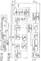
- FIG. 1A there is shown a block diagram of an exemplary hard disk drive 100 coupled with a host device 112. For clarity, some components, such as the servo/actuator motor control, are not shown.
- the drive 100 includes the magnetic platters and spindle motor 102, the read/write heads and actuator assembly 104, pre-amplifiers 106, a read/write channel 108 and a controller 110.
- the pre-amplifiers 106 are coupled with the read/write channel 108 via interfaces 114, 116.
- the controller 110 interfaces with the read/write channel 108 via interfaces 118, 120.
- the host device 112 For reads from the hard disk 100, the host device 112 provides a location identifier which identifies the location of the data on the disk drive, e.g. a cylinder and sector address.
- the controller 110 receives this address and determines the physical location of the data on the platters 102.
- the controller 110 then moves the read/write heads into the proper position for the data to spin underneath the read/write heads 104.
- the read/write head 104 senses the presence or absence of flux reversals, generating a stream of analog signal data. This data is passed to the pre-amplifiers 106 which amplify the signal and pass it to the read/write channel 108 via the interface 114.
- the read/write channel receives the amplified analog waveform from the pre-amplifiers 106 and decodes this waveform into the digital binary data that it represents. This digital binary data is then passed to the controller 110 via the interface 118.
- the controller 110 interfaces the hard drive 100 with the host device 112 and may contain additional functionality, such as caching or error detection/correction functionality, intended to increase the operating speed and/or reliability of the hard drive 100.
- the host device 112 provides the controller 110 with the binary digital data to be written and the location, e.g. cylinder and sector address, of where to write it.
- the controller 110 moves the read/write heads 104 to the proper location and sends the binary digital data to be written to the read/write channel 108 via interface 120.
- the read/write channel 108 receives the binary digital data, encodes it and generates analog signals which are used to drive the read/write head 104 to impart the proper magnetic flux reversals onto the magnetic platters 102 representing the binary digital data.
- the generated signals are passed to the pre-amplifiers 106 via interface 116 which drive the read/write heads 104.
- CMOS complementary metal oxide semiconductor
- PRML Partial Response Maximum Likelihood
- the read/write channel 108 is implemented as an integrated circuit using a complementary metal oxide semiconductor (“CMOS") process at 0.18 micron.
- CMOS processes include processes which use metal gates as well as polysilicon gates.
- CMOS processes include processes which use metal gates as well as polysilicon gates.
- other process technologies and feature sizes may be used and that the circuitry disclosed herein may be further integrated with other circuitry comprising the hard disk electronics such as the hard disk controller logic.
- the read/write channel 108 converts between binary digital information and the analog signals representing the magnetic flux on the platters 102.
- the read/write channel 108 is divided into two main sections, the read path 156 and the write path 158.
- the write path 158 includes a parallel-to-serial converter 144, a run-length-limited (“RLL") encoder 146, a parity encoder 148, a write pre-compensation circuit 150 and a driver circuit 152.
- the parallel-to-serial converter 144 receives data from the host device 112 via interface 120 eight bits at a time.
- the converter 144 serializes the input data and sends the serial bit stream to the RLL encoder 146.
- the RLL encoder 146 encodes the serial bit stream into symbolic binary sequences according to a known run-length limited algorithm for recording on the platters 102.
- the exemplary RLL encoder uses a 32/34 bit symbol code to ensure that flux reversals are properly spaced and that long runs of data without flux reversals are not recorded.
- the RLL encoded data is then passed to the parity encoder 148 which adds a parity bit to the data.
- odd parity is used to ensure that long run's of 0's and 1's are not recorded due to the magnetic properties of such recorded data.
- the parity encoded data is subsequently treated as an analog signal rather than a digital signal.
- the analog signal is passed to a write pre-compensation circuit 150 which dynamically adjusts the pulse widths of the bit stream to account for magnetic distortions in the recording process.
- the adjusted analog signal is passed to a driver circuit 152 which drives the signal to the pre-amplifiers 106 via interface 116 to drive the read/write heads 104 and record the data.
- the exemplary driver circuit 152 includes a pseudo emitter coupled logic (“PECL”) driver circuit which generates a differential output to the pre-amplifiers 106.
- PECL pseudo emitter coupled logic
- the read path 156 of the read/write channel 108 includes an analog portion 162 and a digital portion 164, as illustrated in FIG. 1B .
- the analog portion 162 of the read path 156 is the portion of the read path 156 in which the signal passing through it is primarily analog.
- the analog portion 162 includes an attenuation circuit/input resistance 122, a variable gain amplifier (“VGA”) 124, a magneto-resistive asymmetry linearizer (“MRA”) 126, a continuous time filter (“CTF”) 128, a buffer 130, and an analog to digital converter (“ADC”) 132.
- VGA variable gain amplifier
- MRA magneto-resistive asymmetry linearizer
- CTF continuous time filter
- ADC analog to digital converter
- the digital portion 164 includes a finite impulse response (“FIR”) filter 134, an interpolated timing recovery (“ITR”) circuit 136, a Viterbi algorithm detector 138, a parity decoder 140 and a run-length-limited (“RLL”) decoder 142.
- FIR finite impulse response
- ITR interpolated timing recovery
- RLL run-length-limited
- the amplified magnetic signals sensed from the platters 102 by the read/write head 104 are received by the read/write channel 108 via interface 114.
- the analog signal waveform representing the sensed magnetic signals is first passed through an input resistance 122 which is a switching circuit to attenuate the signal and account for any input resistance.
- the attenuated signal is then passed to a VGA 124 which amplifies the signal.
- the VGA 124 uses (1+X) and (1-X) resistor DACs in gain cells within the VGA 124 to achieve equal gain step size in the logarithmic domain, an example of which is described in greater detail in U.S. Patent Application Serial No. US 2001 0866147, filed on May 25, 2001 , assigned attorney docket no.
- the VGA 124 uses current feedback in the gain cells to achieve equal gain step size in the logarithmic domain, an example of which is described in greater detail in U.S. Patent Application Serial No. US 2001 0865744, filed on May 25, 2001 , assigned attorney docket no. 01 P 09234 US, and titled "High-Bandwidth Low-Voltage Gain-Cell And Voltage Follower Having An Enhanced Transconductance".
- the VGA 124 includes auto zero capacitors that are not in the signal path, an example of which is described in greater detail in U.S. Patent Application Serial No. US 2001 0865389, filed on May 25, 2001 , assigned attorney docket no. 01 P 09221 US, and titled "Active Auto Zero Circuit For Time Continuous Open Loop Amplifiers.
- the amplified signal is then passed to the MRA 126 which adjusts the signal for any distortion created by the recording process.
- the MRA 126 performs the opposite function of the write-pre-compensation circuit 150 in the write path 158.
- the output from the MRA pass to a stemming node 155.
- the stemming node 155 is connected with an offset correction DAC (ODAC) 160.
- ODAC 160 introduces an analog offset, which is proportional to its digital input. Its digital input is controlled by a DC-restore-loop.
- the DC-restore-loop decides based on the output from the ADC 132 if the offset value of the ODAC 160 has to be increased or reduced.
- the goal of the DC-restore-loop is to remove any offset in the analog signal path.
- the analog signal path starts with the signal inputs of the read write channel into the VGA 124 and ends at the ADC 132.
- the DC-restore-loop does this by adding an offset to the analog signal at the output of the MRA 126.
- This offset has ideally the same absolute value as the effective offset in the analog signal path with an opposite sign. By doing so the DC-restore-loop cancels the offset of the analog signal path.
- the signal is next passed through the CTF 128, which is essentially a low pass filter that filters out noise and pre-equalizes the signal by boosting some part of the signal in a pass-band.
- the CTF 128 includes switching Gm cells, an example of which is described in greater detail in U.S. Patent Application Serial No. US 2001 0865863, filed on May 25,2001 , assigned attorney docket no. 01 P 09240 US, and titled "Efficient Low Voltage Switchable Gm Cell In CMOS Technique For Filter and Gain Amplifier Applications," and in U.S. Patent Application Serial No. US 2001 0865649, filed on May 25, 2001 , assigned attorney docket no.
- the CTF 128 includes a separate read filter circuit and a separate servo filter circuit, an example of which is described in greater detail in U.S. Patent Application Serial No. US 2001 0865861, filed on May 25, 2001 , assigned attorney docket no. 01 P 09246 US, and titled "Method and Apparatus For Operating a Continuous Time Filter of a Read/Write Channel For a Hard Disk Drive”.
- the filtered signal is then passed to the ADC 132 via the buffer 130 which samples the analog signal and converts it to a digital form.
- the ADC 132 includes pre-amplifiers 106 with local common mode feedback in analog latches of the ADC 132, an example of which is described in greater detail in U.S. Patent Application Serial No. US 2001 0865856, filed on May 25,2001 , assigned attorney docket no. 01 P 09248 US, and titled “Ultra High Speed Clocked Analog Latch," and in U.S. Patent Application Serial No. US 2001 0865791, filed on May 25, 2001 , assigned attorney docket no. 01 P 09247 US, and titled "Ultra High Speed Clocked Limiting Preamplifier".
- the digital signal Upon passing through the ADC 132, the digital signal is then passed to a FIR filter 134 and then to a timing recovery circuit (ITR) 136.
- the ITR 136 is connected (not shown in the figure) to the FIR filter 134, the MRA 126 and the VGA 124 in a feedback orientation to adjust these circuits according to the signals received to provide timing compensation.
- the exemplary FIR filter 134 is a 10 tap FIR filter.
- the digital signal is then passed to the Viterbi algorithm detector 138 which determines the binary bit pattern represented by the digital signal using digital signal processing techniques.
- the exemplary Viterbi algorithm detector 138 uses a 32 state Viterbi processor.
- the binary data represented by the digital signal is then passed to the parity decoder 140 which removes the parity bit and then to the RLL decoder 142 which decodes the binary RLL encoding symbols back into the actual binary data that they represents This data is then passed to the controller 110 via the interface 118.
- the read/write channel 108 further includes a clock synthesizer 154.
- the clock synthesizer 154 generates the clock signals required for operating the read/write channel 108.
- the exemplary clock synthesizer 154 includes a phased locked loop ("PLL”) with a voltage controlled oscillator and various clock dividers to generate the necessary frequencies.
- PLL phased locked loop
- the clock synthesizer 154 includes a servo clock generator 200, a read/write clock generator 204, a clock multiplexer 208 and an auxiliary clock multiplexer and divider 230, as illustrated in FIG. 2 .
- the servo clock generator 200 generates a servo clock signal 202 and the read/write clock generator 204 generates a read/write clock signal 206.
- the servo clock signal 202 and read/write clock signal 206 then go to a clock multiplexer 208 and an auxiliary clock multiplexer and divider 230.
- the clock multiplexer 208 allows either the servo clock signal 202 or the read/write clock signal 206 to pass through and go to the ADC 132.
- the auxiliary clock multiplexer and divider 230 allows either the servo clock signal 202 or the read/write clock signal 206 to pass through and go to the view DAC 212, as described below.
- the auxiliary clock multiplexer and divider 230 allows the view DAC 212 and the ADC 132 to run at the same time using different clock signals, an example of which is described in greater detail in U.S. Patent Application Serial No. US 2001 0865757, filed on May 25, 2001 , assigned attorney docket no. 01 P 09220 US, and titled "Method and System For Utilizing a View DAC To Calibrate a Continuous Time Filter".
- the read/write clock generator 204 uses no divider at reference frequency inputs of phase locked loops for generating the read clock signal 206, an example of which is described in greater detail in U.S. Patent Application Serial No. 09/676,277, filed September 28,2000 , assigned attorney docket no. 00 P 7955 US, and titled "High Resolution, Low Jitter Frequency Synthesizer”.
- the servo clock generator 200 also referred to as “servo clock generation” uses no divider at reference frequency inputs of phase locked loops for generating the servo clock signal 202, an example of which is described in greater detail in U.S. Patent Application Serial No. 09/676,277, filed September 28, 2000 , assigned attorney docket no. 00 P 7955 US, and titled "High Resolution, Low Jitter Frequency Synthesizer”.
- the read/write clock generator 204 includes read/write phased locked loops having a feedback path.
- the read/write clock generator 204 uses a fractional divider in the feedback path of the read/write phased locked loops to achieve low frequency programming step sizes, an example of which is described in greater detail in U.S. Patent Application Serial No. 09/676,277, filed September 28, 2000 , assigned attorney docket no. 00 P 7955 US, and titled "High Resolution, Low Jitter Frequency Synthesizer".
- the read/write clock generator 204 uses a low voltage charge pump, an example of which is described in greater detail in U.S. Patent Application Serial No. US 2001 0865610, filed on May 25, 2001 , assigned attorney docket no. 01 P 09228, and titled "Low Voltage Charge Pump for Synthesizer/PLL”.
- the read/write clock generator 204 uses an offset canceled charge-pump-based-phase-frequency detector, an example of which is described in greater detail in U.S. Patent Application Serial No. US 2001 0865406, filed on May 25,2001 , assigned attorney docket no. 01 P 09233 US, and titled "Offset Calibration of Charge Pump Based Phase Detector for Synthesizer/PLL".
- the read/write clock generator 204 includes a Voltage Controlled Oscillator (VCO) 250 that is used for read/write clock generation.
- VCO Voltage Controlled Oscillator
- the read/write clock generator 204 uses a delay unit with four transistors as a delay unit for the VCO 250, an example of which is described in greater detail in U.S. Patent Application Serial No. US 2001 0865269, filed on May 25, 2001 , assigned attorney docket no. 01 P 09241 US, and titled "Differential CMOS Controlled Delay Unit".
- the read/write clock generator 204 uses a delay unit to build a VCO 250 with only two delay stages, an example of which is described in greater detail in U.S. Patent Application Serial No.
- the read/write clock generator 204 uses a fully functional VCO 250 which has only one port for receiving both the power supply voltage and the control input signal to the VCO 250, an example of which is described in greater detail in U.S. Patent Application Serial No. US 2001 0866269, filed on May 25,2001 , assigned attorney docket no. 01 P 09241 US, and titled "Differential CMOS Controlled Delay Unit".
- the read/write clock generator 204 uses a VCO buffer that includes only one source follower and a current feedback loop, an example of which is described in greater detail in U.S. Patent Application Serial No. US 2001 0866178, filed on May 25,2001 , assigned attorney docket no. 01 P 09239 US, and titled "Efficient Current Feedback Buffer".
- the read/write clock generator 204 includes a multiphase multiplexer that only has one or two NMOS transistors in each signal path of each phase and a pull up PMOS transistor operating as a pull up resistor, an example of which is described in greater detail in U.S. Patent Application Serial No. US 2001 0866264, filed on May 25, 2001 , assigned attorney docket no. 01 P 09237 US, and titled "High-Speed Multiplexer".
- the analog portion 162 of the read path 156 includes a write pre-compensation circuit 262, which dynamically adjusts the pulse widths of the bit stream to account for magnetic distortions in the recording process, as illustrated in Figure 2 .
- the synthesizer 154 and more specifically, the read/write clock generator 204 is connected with the write pre-compensation circuit 262. Additionally, the write pre-compensation circuit 262 receives write data 264 from the digital portion 164 of the read path 156 of the read/write channel 108. The write pre-compensation circuit 262 outputs write data with pre-compensation 268, which is received by write output drivers 272.
- the read/write clock generator 204 generates a multiphase output signal 270 using the VCO 250.
- the multiphase output signal 270 preferably includes at least four signals of varying phase, as illustrated in Figure 2 .
- the multiphase output signal 270 is then passed to and used by the write pre-compensation circuit 262.
- the write pre-compensation circuit 262 interpolates one or two times between difference phases of the VCO 250, an example of which is described in greater detail in U.S. Patent Application Serial No. US 2001 0865786, filed on May 25, 2001 , assigned attorney docket no. 01 P 09230 US, and titled "Method and System for Managing a Pulse Width of a Signal Pulse".
- the write pre-compensation circuit 262 uses a write compensation technique that has a digital zero phase restart, an example of which is described in greater detail in U.S. Patent Application Serial No. US 2001 0865787, filed on May 25, 2001 , assigned attorney docket no. 01 P 09227 US, and titled "High Speed Digital Zero Phase Restart for a Multiphase Clock".
- the analog portion 162 of the read path 156 further includes a 7 bit digital multiplexer 228, a view DAC 212, an analog multiplexer 216, high speed analog pin driver buffers 218, an analog comparator 220, and a successive approximation register 222, as illustrated in Figure 2 .
- the 7 bit digital multiplexer 228 receives 7 bit view DAC data from the digital portion of the read/write channel 108 and receives a 7 bit auxiliary ADC output signal 224 from the successive approximation register 222, and decides which signal should pass to the view DAC 212.
- the view DAC 212 received the signal from the 7 bit digital multiplexer 228 and an additional clock signal from the auxiliary clock multiplexer and divider 230 and generates a view DAC output signal 214.
- the view DAC output signal 214 then passes to the analog comparator 220 and the analog multiplexer 216.
- the analog multiplexer 216 receives signals from the outputs of the VGA 124, the MRA 126, the CTF 128, and the buffer 130. Upon receiving all these signals, the analog multiplexer 216 then decides which signal to output, and outputs one of these signals to the high speed analog pin driver buffers 218.
- the high speed analog pin driver buffers 218 also receive a disable/power down signal.
- the read/write channel is able to multiplex the view DAC output 214 and an AC test bus output to the same pins, an example of which is described in greater detail in U.S. Patent Application Serial No. US 2001 0865611, filed on May 25, 2001 , assigned attorney docket no. 01 P 09250 US, and titled "InpudOutput Multiplex System for a Read/Write Channel in a Disk Drive".
- the analog comparator 220 receives the view DAC output signal 214 and compares it with the output from the high speed analog pin driver buffers 218 and generates an output signal that is passed to the successive approximation register 222.
- the successive approximation register 222 together with the view DAC 212 and the analog comparator 220, forms an auxiliary analog to digital converter (ADC).
- ADC auxiliary analog to digital converter
- the successive approximation register 222 decides, based on the output of the analog comparator 220, the voltage that should be generated in the next clock cycle by the view DAC 212 for purposes of comparison with the analog voltage being input to the analog comparator 220.
- the successive approximation register 222 contains the output of the analog to digital converter 132.
- the successive approximation register 222 then generates the 7 bit auxiliary ADC output signal 224 that is passed to the digital portion 164 and to the 7 bit digital multiplexer 228, as illustrated in Figure 2 .
- the analog portion 162 of the read path 156 further includes a second analog multiplexer 274, write output drivers 272, and a DC test bus enable switch 276, as illustrated in Figure 2 .
- the second analog multiplexer 274 receives the signal output from the high speed analog pin driver buffers 218 and the signal from the analog multiplexer 216 and decides which signal should pass to the analog comparator 220.
- the output of the high speed analog pin driver buffers 218 is also connected with the output of the write output drivers 272, as illustrated in Figure 2 .
- the write output drivers 272 receive the write data with pre-compensation 268 from the write pre-compensation circuit, the write data 264 from the digital portion, and a disable/power down write driver signal 266.
- the output of the write output drivers 272 is connected with the output of the DC test bus enable switch 276.
- the DC test bus enable switch 276 is in communication with internal analog nodes, as illustrated in Figure 2 .
- the read/write channel 108 is able to multiplex write data outputs, a DC test bus input, and a DC test bus output to the same pins, an example of which is described in greater detail in U.S. Patent Application Serial No. US 2001 0865611, filed on May 25, 2001 , assigned attorney docket no. 01 P 09250 US, and titled "Input/Output Multiplex System for a Read/Write Channel in a Disk Drive”. Additionally, using the above described circuitry, the read/write channel 108 is able to reuse the view DAC 212 to build an auxiliary analog to digital converter, an example of which is described in greater detail in U.S. Patent Application Serial No. US 2001 0865651, on May 25, 2001 , assigned attorney docket no. 01 P 09249 US, and titled "Diagnostic System for a Read/Write Channel in a Disk Driver".
- the analog portion 162 of the read path 156 further includes a first view DAC feedback circuit 278 and a second view DAC feedback circuit 280 which allows the view DAC output signal 214 to enter the input of the VGA 124 or the input of the CTF 128, as illustrated in Figure 3 , an example of which is described in greater detail in U.S. Patent Application Serial No. US 2001 0865757, filed on May 25,2001 , assigned attorney docket no. 01 P 09220 US, and titled "Method and System For Utilizing a View DAC To Calibrate a Continuous Time Filter".
- the read/write channel 108 and in particular, the analog portion 162 and the clock synthesizer 154, are supplied power from a highly regulated power supply 260, as illustrated in Figure 2 .
- the highly regulated power supply 260 supplies power having a narrow voltage range to the read/write channel 108.
- a narrow voltage range is a voltage range that is within +/- 7% of the nominal voltage, and more preferably, within +/- 3% of the nominal voltage.
- Highly regulated power supply 260 includes a chopper stabilized bandgap 240, an integrated voltage regulator 244, a negative power supply voltage 246, resistive voltage dividers 248, an pass transistor 258, and an external power supply 238.
- the chopper stabilized bandgap 240, the integrated voltage regulator 244, the negative power supply voltage 246, and the resistive voltage dividers 248 are located within the read/write channel 108 while the pass transistor 258 and the external power supply 238 are not located within the read/write channel 108, as illustrated in Figure 2 .
- the external power supply 238 generates a negative high power supply voltage 246 and a positive high power supply voltage 254.
- the negative high power supply voltage 246 and the positive high power supply voltage 254 are about 2.4 volts +/- 10%.
- the positive high power supply voltage 254 is supplied to the chopper stabilized bandgap 240 and the negative high power supply voltage 246 passes through a resistive voltage divider 248 and is then supplied to a negative input of the integrated voltage regulator 244, as illustrated in Figure 2 .
- the chopper stabilized bandgap 240 generates a reference voltage 242 from the positive high power supply voltage 254.
- the reference voltage 242 has a high absolute accuracy and a low temperature coefficient, so that even if the temperature of the surrounding environment changes, the reference voltage 242 stays within a narrow voltage range, that is a voltage range that is within +/- 7% of the nominal voltage for the reference voltage 242, and more preferably, +/- 3% of the nominal voltage for the reference voltage 242.
- the reference voltage 242 is supplied to a positive input of the integrated voltage regulator 244.
- the integrated voltage regulator 244 receives the reference voltage 242 and the negative high power supply voltage 246, and generates an output voltage 253.
- the integrated voltage regulator 244 increases the value of the output voltage 253 until the value of the reference voltage 242 entering the positive input and the value of the negative high power supply voltage 246 entering the negative input, are the essentially same.
- the output voltage 253 enters the pass transistor 258 at a base of the pass transistor 258.
- Positive high power supply voltage 254 enters the pass transistor 258, as illustrated in Figure 2 . If the pass transistor 258 is a NPN-type transistor, then positive high power supply voltage 254 enters the pass transistor 258 at a collector of the pass transistor 258.
- positive high power supply voltage 254 enters the pass transistor 258 at an emitter of the pass transistor 258.
- An external signal 255 leaves the pass transistor 258 either at an emitter, if the pass transistor 258 is a NPN-type transistor, or at a collector, if the pass transistor 258 is a PNP-type transistor.
- a portion of the external signal 255 is transmitted through a resistive voltage divider 248 to the negative input of the integrated voltage divider 244, while another portion of the external signal 255 is supplied to the analog portion 162 and the clock synthesizer 154 as an internal positive low power supply voltage 256.
- the internal positive low power supply voltage 256 has a narrow voltage range.
- the internal positive low power supply voltage 256 is less than 2.2 volts, and more preferably less than 2.0 volts. In one embodiment, the internal positive low power supply voltage 256 has a value of 1.92 volts +/- 3%. While the above described pass transistor 258 is either a PNP-transistor, or a NPN transistor, the pass transistor 258 may include any transistor known to those skilled in the art, such as an MOS transistor, a NMOS transistor, or a PMOS transistor.
- the highly regulated power supply 260 supplies power having a single, low voltage range to the read/write channel 108.
- Operating the read/write channel 108 in a single, low voltage range would prevent the use of additional circuitry, would eliminate verification and simulations performed on the analog portion 162 and the clock synthesizer 154, and would lower the power consumption of the read/write channel 108.
- the time required to design the read/write channel 108 would be decreased.
- the read/write channel 108 including high voltage transistors that operate at a voltage range of between 1.86 volts and 1.98 volts (1.92 volts +/- 3%) and low voltage transistors that operate at a voltage range of between 1.62 volts and 1.98 volts (1.8 volts +/- 10%), wherein the highly regulated power supply 260 supplies power having a single, low voltage range of between 1.86 volts and 1.98 volts (1.92 volts +/- 3%) to the read/write channel 108.
- the low voltage transistors have a maximum voltage rating.
- the maximum voltage rating is the maximum voltage at which the low voltage transistors may operate at.
- the highly regulated power supply 260 supplies power to the analog portion 162 and the clock synthesizer 154 having a nominal value between 95% and 100% of the maximum voltage rating of the low voltage transistors. So, for example, if the low voltage transistors have a maximum voltage rating of 1.98 volts, then the highly regulated power supply 260 would supply power to the analog portion 162 and the clock synthesizer 154 which is between 1.88 volts and 1.98 volts.
Landscapes
- Engineering & Computer Science (AREA)
- Signal Processing (AREA)
- Digital Magnetic Recording (AREA)
- Signal Processing For Digital Recording And Reproducing (AREA)
Description
- Computer hard disk drives, also known as fixed disk drives or hard drives, have become a de facto standard data storage component of modem computer systems and are making further inroads into modem consumer electronics as well. Their proliferation can be directly attributed to their low cost, high storage capacity and high reliability, in addition to wide availability, low power consumption, high data transfer speeds and decreasing physical size.
- These disk drives typically consist of one or more rotating magnetic platters encased within an environmentally controlled housing that further includes all of the electronics and mechanics to read and write data and interface with other devices. Read/write heads are positioned above each of the platters, and typically on each face, to record and read data. The electronics of a hard disk drive are coupled with these read/write heads and include numerous components to control the position of the heads and generate or sense the electromagnetic fields representing data. These components receive data from a host device, such as a personal computer, and translate that data into magnetic encodings written onto the disk platters by the heads. Further, when a host device requests data from the drive, the electronics locate the desired data, sense the magnetic encodings which represent that data and translate those encodings back into the binary digital information which the host device can understand. Further, error detection and correction algorithms are applied to ensure accurate storage and retrieval of data.
- One area in which significant advancements have been made has been in the area of read/write head technology and the methods of interpreting the magnetic fluctuations sensed by these heads. The read/write head, of which a typical hard disk has several, is the interface between magnetic platters and the disk drive electronics. The read/write head actually reads and writes the magnetically encoded data as areas of magnetic flux on the platters. Data, consisting of binary 1's and 0's, are encoded by sequences of the presence or absence of flux reversals recorded or detected by the read/write head. A flux reversal is a change in the magnetic flux in two contiguous areas of the disk platter. Traditional hard drives read data off the platters by detecting the voltage peak imparted in the read/write head when a flux reversal passes underneath the read/write head as the platters rotate. This is known as "peak detection." However, increasing storage densities require reduced peak amplitudes and better signal discrimination and higher platter rotational speeds are pushing the peaks closer together thus making peak detection more difficult to accomplish.
- Magneto-resistive ("MR") read/write heads have been developed with increased sensitivity to sense smaller amplitude magnetic signals and with increased signal discrimination to address some of the problems with increasing storage densities. In addition, another technology, known as Partial Response Maximum Likelihood ("PRML"), has been developed to further address the problems with peak detection as densities and rotational speeds increase. Borrowed from communications technology, PRML is an algorithm implemented in the disk drive electronics to interpret the magnetic signals sensed by the read/write heads. PRML-based disk drives read the analog waveforms generated by the magnetic flux reversals stored on the disk. However, instead of looking for peak values to indicate flux reversals, PRML-based drives digitally sample this analog waveform (the "Partial Response") and use advanced signal processing technologies to determine the bit pattern represented by that wave form (the "Maximum Likelihood"). This technology, in conjunction magneto-resistive ("MR") heads, have permitted manufacturers to further increase data storage densities. PRML technology further tolerates more noise in the sensed magnetic signals permitting the use of lower quality platters and read/write heads which increases manufacturing yields and lowers costs.
- The read/write heads of the hard disk drive are coupled with a device called a read/write channel. Herein, the phrase "coupled with" is defined to mean directly connected to or indirectly connected with through one or more intermediate components. Such intermediate components may include both hardware and software based components. The read/write channel converts binary/digital data from the host device into the electrical impulses which drive the read/write head to magnetically record the data to the disk drive platters. Further, the read/write channel receives the analog waveform magnetically sensed by the read/write heads and converts that waveform back into the binary/digital data stored on the drive.
- With many different drives available from multiple manufacturers, hard disk drives are typically differentiated by factors such as cost/megabyte of storage, data transfer rate, power requirements and form factor (physical dimensions) with the bulk of competition based on cost. With most competition between hard disk drive manufacturers coming in the area of cost, there is a need for enhanced hard disk drive components which prove cost effective in increasing supplies and driving down manufacturing costs all while increasing storage capacity, operating speed, reliability and power efficiency.
- One area in which power efficiency can be increased is with the read/write channel of the hard drive. The read/write channel of the hard drive typically includes an analog portion, which is used to convert digital signals received from a controller to analog signals which then get sent to the read/write heads. The analog portion may also be used to receive analog signals from the read/write heads and convert them into digital signals.
- Typically, the analog portion of the read/write
channel 108 is manufactured using one of two methods. The first method is to use only high voltage transistors which all operate within the same voltage range. However, high voltage transistors require a lot of power, are relatively slow, and do not scale so well with a CMOS manufacturing process. The second method is to use both high voltage transistors and low voltage transistors and use a power supply voltage, which is substantially higher than the maximum rating for the low voltage transistors. Low voltage transistors operate at a higher speed, occupy less silicon area, and consume less power than high voltage transistors. Typically, low voltage transistors are used in a core area of a circuit and high voltage transistors are used in an I/O area of the circuit. However, since the high voltage transistors operate at a higher voltage range than the low voltage transistors, verification and simulations must be performed on the analog portion to insure that the low voltage transistors never receive more voltage than is required for them to operate. For example, the analog portion may include high voltage transistors that operate at a voltage range of between 2.16 volts and 2.64 volts (2.4 volts +/- 10%), and low voltage transistors that operate at a lower voltage range, such as between 1.62 volts and 1.98 volts (1.8 volts +/- 10%). In this example, since the analog portion is typically supplied a voltage that is within a single range, such as a voltage of 2.4 volts +/- 10%, verification and simulations must be performed on the analog portion to insure that the low voltage transistors never receive more voltage than is required for them to operate. Moreover, additional circuitry is placed inside the analog portion to further insure that the low voltage transistors never receive more voltage than is required for them to operate. The additional circuitry, and the verification and the simulations that must be performed on the analog portion, in turn, increase the time required to design the read/write channel. - The above mentioned problems are solved by the read/write channel claimed in
claim 1 and by the method for operating a read/write channel claimed in claim 22. - Advantageous further embodiments are claimed in the subclaims.
-
-
Figure 1A depicts a block diagram of an exemplary hard disk drive coupled with a host device. -
Figure 1B depicts a block diagram of a read/write channel for use with the disk drive ofFigure 1A . -
Figure 2 depicts a block diagram of a portion of a read path of a read/write channel, according to one preferred embodiment. -
Figure 3 depicts a block diagram of a portion of a read path of a read/write channel, according to one preferred embodiment. - The embodiments described herein relate to a PRML-based read/write channel device for hard disk drive controllers. The read/write channel is a device coupled with the read/write heads of the hard disk drive. Herein, the phrase "coupled with" is defined to mean directly connected to or indirectly connected with through one or more intermediate components. Such intermediate components may include both hardware and software based components. The read/write channel converts binary/digital data from the host device into the electrical impulses which drive the read/write head to magnetically record the data to the disk drive platters. Further, the read/write channel receives the analog waveform magnetically sensed by the read/write heads and converts that waveform back into the binary/digital data stored on the drive.
- Referring to
Figure 1A , there is shown a block diagram of an exemplaryhard disk drive 100 coupled with ahost device 112. For clarity, some components, such as the servo/actuator motor control, are not shown. Thedrive 100 includes the magnetic platters andspindle motor 102, the read/write heads andactuator assembly 104, pre-amplifiers 106, a read/writechannel 108 and acontroller 110. The pre-amplifiers 106 are coupled with the read/writechannel 108 viainterfaces controller 110 interfaces with the read/writechannel 108 viainterfaces - For reads from the
hard disk 100, thehost device 112 provides a location identifier which identifies the location of the data on the disk drive, e.g. a cylinder and sector address. Thecontroller 110 receives this address and determines the physical location of the data on theplatters 102. Thecontroller 110 then moves the read/write heads into the proper position for the data to spin underneath the read/write heads 104. As the data spins underneath the read/write head 104, the read/write head 104 senses the presence or absence of flux reversals, generating a stream of analog signal data. This data is passed to thepre-amplifiers 106 which amplify the signal and pass it to the read/write channel 108 via theinterface 114. As will be discussed below, the read/write channel receives the amplified analog waveform from thepre-amplifiers 106 and decodes this waveform into the digital binary data that it represents. This digital binary data is then passed to thecontroller 110 via theinterface 118. Thecontroller 110 interfaces thehard drive 100 with thehost device 112 and may contain additional functionality, such as caching or error detection/correction functionality, intended to increase the operating speed and/or reliability of thehard drive 100. - For write operations, the
host device 112 provides thecontroller 110 with the binary digital data to be written and the location, e.g. cylinder and sector address, of where to write it. Thecontroller 110 moves the read/write heads 104 to the proper location and sends the binary digital data to be written to the read/write channel 108 viainterface 120. The read/write channel 108 receives the binary digital data, encodes it and generates analog signals which are used to drive the read/write head 104 to impart the proper magnetic flux reversals onto themagnetic platters 102 representing the binary digital data. The generated signals are passed to thepre-amplifiers 106 viainterface 116 which drive the read/write heads 104. - Referring to
Figure 1B , there is shown an exemplary read/write channel 108 supporting Partial Response Maximum Likelihood ("PRML") encoding technology for use with thehard disk drive 100 ofFigure 1A . For clarity, some components have been omitted. The read/write channel 108 is implemented as an integrated circuit using a complementary metal oxide semiconductor ("CMOS") process at 0.18 micron. It will be appreciated that CMOS processes include processes which use metal gates as well as polysilicon gates. It will further be appreciated that other process technologies and feature sizes may used and that the circuitry disclosed herein may be further integrated with other circuitry comprising the hard disk electronics such as the hard disk controller logic. As was described, the read/write channel 108 converts between binary digital information and the analog signals representing the magnetic flux on theplatters 102. The read/write channel 108 is divided into two main sections, theread path 156 and thewrite path 158. - The
write path 158 includes a parallel-to-serial converter 144, a run-length-limited ("RLL")encoder 146, aparity encoder 148, awrite pre-compensation circuit 150 and adriver circuit 152. The parallel-to-serial converter 144 receives data from thehost device 112 viainterface 120 eight bits at a time. The converter 144 serializes the input data and sends the serial bit stream to theRLL encoder 146. TheRLL encoder 146 encodes the serial bit stream into symbolic binary sequences according to a known run-length limited algorithm for recording on theplatters 102. The exemplary RLL encoder uses a 32/34 bit symbol code to ensure that flux reversals are properly spaced and that long runs of data without flux reversals are not recorded. The RLL encoded data is then passed to theparity encoder 148 which adds a parity bit to the data. In theexemplary parity encoder 148, odd parity is used to ensure that long run's of 0's and 1's are not recorded due to the magnetic properties of such recorded data. The parity encoded data is subsequently treated as an analog signal rather than a digital signal. The analog signal is passed to awrite pre-compensation circuit 150 which dynamically adjusts the pulse widths of the bit stream to account for magnetic distortions in the recording process. The adjusted analog signal is passed to adriver circuit 152 which drives the signal to thepre-amplifiers 106 viainterface 116 to drive the read/write heads 104 and record the data. Theexemplary driver circuit 152 includes a pseudo emitter coupled logic ("PECL") driver circuit which generates a differential output to the pre-amplifiers 106. - The
read path 156 of the read/write channel 108 includes ananalog portion 162 and a digital portion 164, as illustrated inFIG. 1B . Theanalog portion 162 of the readpath 156 is the portion of the readpath 156 in which the signal passing through it is primarily analog. Theanalog portion 162 includes an attenuation circuit/input resistance 122, a variable gain amplifier ("VGA") 124, a magneto-resistive asymmetry linearizer ("MRA") 126, a continuous time filter ("CTF") 128, abuffer 130, and an analog to digital converter ("ADC") 132. The digital portion 164 of the readpath 156 is the portion of the readpath 156 in which the signal passing through it is primarily digital. The digital portion 164 includes a finite impulse response ("FIR")filter 134, an interpolated timing recovery ("ITR")circuit 136, aViterbi algorithm detector 138, aparity decoder 140 and a run-length-limited ("RLL")decoder 142. - The amplified magnetic signals sensed from the
platters 102 by the read/write head 104 are received by the read/write channel 108 viainterface 114. The analog signal waveform representing the sensed magnetic signals is first passed through aninput resistance 122 which is a switching circuit to attenuate the signal and account for any input resistance. The attenuated signal is then passed to aVGA 124 which amplifies the signal. In one embodiment, theVGA 124 uses (1+X) and (1-X) resistor DACs in gain cells within theVGA 124 to achieve equal gain step size in the logarithmic domain, an example of which is described in greater detail in U.S. Patent Application Serial No.US 2001 0866147, filed on May 25, 2001 , assigned attorney docket no. 01 P 09222 US, and titled "Programmable Logarithmic Gain Adjustment for Open-Loop Amplifiers". In one embodiment, theVGA 124 uses current feedback in the gain cells to achieve equal gain step size in the logarithmic domain, an example of which is described in greater detail in U.S. Patent Application Serial No.US 2001 0865744, filed on May 25, 2001 , assigned attorney docket no. 01 P 09234 US, and titled "High-Bandwidth Low-Voltage Gain-Cell And Voltage Follower Having An Enhanced Transconductance". Preferably, theVGA 124 includes auto zero capacitors that are not in the signal path, an example of which is described in greater detail in U.S. Patent Application Serial No.US 2001 0865389, filed on May 25, 2001 , assigned attorney docket no. 01 P 09221 US, and titled "Active Auto Zero Circuit For Time Continuous Open Loop Amplifiers. - Upon passing through
VGA 124, the amplified signal is then passed to theMRA 126 which adjusts the signal for any distortion created by the recording process. Essentially, theMRA 126 performs the opposite function of the write-pre-compensation circuit 150 in thewrite path 158. In one preferred embodiment, the output from the MRA pass to a stemmingnode 155. The stemmingnode 155 is connected with an offset correction DAC (ODAC) 160. TheODAC 160 introduces an analog offset, which is proportional to its digital input. Its digital input is controlled by a DC-restore-loop. The DC-restore-loop decides based on the output from theADC 132 if the offset value of theODAC 160 has to be increased or reduced. The goal of the DC-restore-loop is to remove any offset in the analog signal path. The analog signal path starts with the signal inputs of the read write channel into theVGA 124 and ends at theADC 132. The DC-restore-loop does this by adding an offset to the analog signal at the output of theMRA 126. This offset has ideally the same absolute value as the effective offset in the analog signal path with an opposite sign. By doing so the DC-restore-loop cancels the offset of the analog signal path. - The signal is next passed through the
CTF 128, which is essentially a low pass filter that filters out noise and pre-equalizes the signal by boosting some part of the signal in a pass-band. Preferably, theCTF 128 includes switching Gm cells, an example of which is described in greater detail in U.S. Patent Application Serial No.US 2001 0865863, filed on May 25,2001 , assigned attorney docket no. 01 P 09240 US, and titled "Efficient Low Voltage Switchable Gm Cell In CMOS Technique For Filter and Gain Amplifier Applications," and in U.S. Patent Application Serial No.US 2001 0865649, filed on May 25, 2001 , assigned attorney docket no. 01 P 09245 US, and titled "Method and Apparatus for Calibrating a Gm Cell Utilizing a Replica Gm Cell". In one embodiment, theCTF 128 includes a separate read filter circuit and a separate servo filter circuit, an example of which is described in greater detail in U.S. Patent Application Serial No.US 2001 0865861, filed on May 25, 2001 , assigned attorney docket no. 01 P 09246 US, and titled "Method and Apparatus For Operating a Continuous Time Filter of a Read/Write Channel For a Hard Disk Drive". The filtered signal is then passed to theADC 132 via thebuffer 130 which samples the analog signal and converts it to a digital form. Preferably, theADC 132 includespre-amplifiers 106 with local common mode feedback in analog latches of theADC 132, an example of which is described in greater detail in U.S. Patent Application Serial No.US 2001 0865856, filed on May 25,2001 , assigned attorney docket no. 01 P 09248 US, and titled "Ultra High Speed Clocked Analog Latch," and in U.S. Patent Application Serial No.US 2001 0865791, filed on May 25, 2001 , assigned attorney docket no. 01 P 09247 US, and titled "Ultra High Speed Clocked Limiting Preamplifier". - Upon passing through the
ADC 132, the digital signal is then passed to aFIR filter 134 and then to a timing recovery circuit (ITR) 136. TheITR 136 is connected (not shown in the figure) to theFIR filter 134, theMRA 126 and theVGA 124 in a feedback orientation to adjust these circuits according to the signals received to provide timing compensation. Theexemplary FIR filter 134 is a 10 tap FIR filter. The digital signal is then passed to theViterbi algorithm detector 138 which determines the binary bit pattern represented by the digital signal using digital signal processing techniques. The exemplaryViterbi algorithm detector 138 uses a 32 state Viterbi processor. The binary data represented by the digital signal is then passed to theparity decoder 140 which removes the parity bit and then to theRLL decoder 142 which decodes the binary RLL encoding symbols back into the actual binary data that they represents This data is then passed to thecontroller 110 via theinterface 118. - The read/
write channel 108 further includes aclock synthesizer 154. Theclock synthesizer 154 generates the clock signals required for operating the read/write channel 108. Theexemplary clock synthesizer 154 includes a phased locked loop ("PLL") with a voltage controlled oscillator and various clock dividers to generate the necessary frequencies. - In one preferred embodiment, the
clock synthesizer 154 includes aservo clock generator 200, a read/write clock generator 204, aclock multiplexer 208 and an auxiliary clock multiplexer anddivider 230, as illustrated inFIG. 2 . Theservo clock generator 200 generates aservo clock signal 202 and the read/write clock generator 204 generates a read/write clock signal 206. Theservo clock signal 202 and read/write clock signal 206 then go to aclock multiplexer 208 and an auxiliary clock multiplexer anddivider 230. Theclock multiplexer 208 allows either theservo clock signal 202 or the read/write clock signal 206 to pass through and go to theADC 132. The auxiliary clock multiplexer anddivider 230 allows either theservo clock signal 202 or the read/write clock signal 206 to pass through and go to theview DAC 212, as described below. The auxiliary clock multiplexer anddivider 230 allows theview DAC 212 and theADC 132 to run at the same time using different clock signals, an example of which is described in greater detail in U.S. Patent Application Serial No.US 2001 0865757, filed on May 25, 2001 , assigned attorney docket no. 01 P 09220 US, and titled "Method and System For Utilizing a View DAC To Calibrate a Continuous Time Filter". - In one preferred embodiment, the read/
write clock generator 204, also referred to as "read/write clock generation," uses no divider at reference frequency inputs of phase locked loops for generating the readclock signal 206, an example of which is described in greater detail inU.S. Patent Application Serial No. 09/676,277, filed September 28,2000 servo clock generator 200, also referred to as "servo clock generation," uses no divider at reference frequency inputs of phase locked loops for generating theservo clock signal 202, an example of which is described in greater detail inU.S. Patent Application Serial No. 09/676,277, filed September 28, 2000 - In one preferred embodiment, the read/
write clock generator 204 includes read/write phased locked loops having a feedback path. The read/write clock generator 204 uses a fractional divider in the feedback path of the read/write phased locked loops to achieve low frequency programming step sizes, an example of which is described in greater detail inU.S. Patent Application Serial No. 09/676,277, filed September 28, 2000 - In one embodiment, the read/
write clock generator 204 uses a low voltage charge pump, an example of which is described in greater detail in U.S. Patent Application Serial No.US 2001 0865610, filed on May 25, 2001 , assigned attorney docket no. 01 P 09228, and titled "Low Voltage Charge Pump for Synthesizer/PLL". - In one embodiment, the read/
write clock generator 204 uses an offset canceled charge-pump-based-phase-frequency detector, an example of which is described in greater detail in U.S. Patent Application Serial No.US 2001 0865406, filed on May 25,2001 , assigned attorney docket no. 01 P 09233 US, and titled "Offset Calibration of Charge Pump Based Phase Detector for Synthesizer/PLL". - In one embodiment, the read/
write clock generator 204 includes a Voltage Controlled Oscillator (VCO) 250 that is used for read/write clock generation. Preferably, the read/write clock generator 204 uses a delay unit with four transistors as a delay unit for theVCO 250, an example of which is described in greater detail in U.S. Patent Application Serial No.US 2001 0865269, filed on May 25, 2001 , assigned attorney docket no. 01 P 09241 US, and titled "Differential CMOS Controlled Delay Unit". In one embodiment, the read/write clock generator 204 uses a delay unit to build aVCO 250 with only two delay stages, an example of which is described in greater detail in U.S. Patent Application Serial No.US 2001 0866269, filed on May 25,2001 , assigned attorney docket no. 01 P 09241 US, and titled "Differential CMOS Controlled Delay Unit". In one embodiment, the read/write clock generator 204 uses a fullyfunctional VCO 250 which has only one port for receiving both the power supply voltage and the control input signal to theVCO 250, an example of which is described in greater detail in U.S. Patent Application Serial No.US 2001 0866269, filed on May 25,2001 , assigned attorney docket no. 01 P 09241 US, and titled "Differential CMOS Controlled Delay Unit". In one embodiment, the read/write clock generator 204 uses a VCO buffer that includes only one source follower and a current feedback loop, an example of which is described in greater detail in U.S. Patent Application Serial No.US 2001 0866178, filed on May 25,2001 , assigned attorney docket no. 01 P 09239 US, and titled "Efficient Current Feedback Buffer". - In one embodiment, the read/
write clock generator 204 includes a multiphase multiplexer that only has one or two NMOS transistors in each signal path of each phase and a pull up PMOS transistor operating as a pull up resistor, an example of which is described in greater detail in U.S. Patent Application Serial No.US 2001 0866264, filed on May 25, 2001 , assigned attorney docket no. 01 P 09237 US, and titled "High-Speed Multiplexer". - In one embodiment, the
analog portion 162 of the readpath 156 includes awrite pre-compensation circuit 262, which dynamically adjusts the pulse widths of the bit stream to account for magnetic distortions in the recording process, as illustrated inFigure 2 . Thesynthesizer 154, and more specifically, the read/write clock generator 204 is connected with thewrite pre-compensation circuit 262. Additionally, thewrite pre-compensation circuit 262 receives writedata 264 from the digital portion 164 of the readpath 156 of the read/write channel 108. Thewrite pre-compensation circuit 262 outputs write data withpre-compensation 268, which is received bywrite output drivers 272. - In one embodiment, the read/
write clock generator 204 generates amultiphase output signal 270 using theVCO 250. Themultiphase output signal 270 preferably includes at least four signals of varying phase, as illustrated inFigure 2 . Themultiphase output signal 270 is then passed to and used by thewrite pre-compensation circuit 262. In one embodiment, thewrite pre-compensation circuit 262 interpolates one or two times between difference phases of theVCO 250, an example of which is described in greater detail in U.S. Patent Application Serial No.US 2001 0865786, filed on May 25, 2001 , assigned attorney docket no. 01 P 09230 US, and titled "Method and System for Managing a Pulse Width of a Signal Pulse". In one embodiment, thewrite pre-compensation circuit 262 uses a write compensation technique that has a digital zero phase restart, an example of which is described in greater detail in U.S. Patent Application Serial No.US 2001 0865787, filed on May 25, 2001 , assigned attorney docket no. 01 P 09227 US, and titled "High Speed Digital Zero Phase Restart for a Multiphase Clock". - In one preferred embodiment, the
analog portion 162 of the readpath 156 further includes a 7 bitdigital multiplexer 228, aview DAC 212, ananalog multiplexer 216, high speed analog pin driver buffers 218, ananalog comparator 220, and a successive approximation register 222, as illustrated inFigure 2 . The 7 bitdigital multiplexer 228 receives 7 bit view DAC data from the digital portion of the read/write channel 108 and receives a 7 bit auxiliary ADC output signal 224 from the successive approximation register 222, and decides which signal should pass to theview DAC 212. Theview DAC 212 received the signal from the 7 bitdigital multiplexer 228 and an additional clock signal from the auxiliary clock multiplexer anddivider 230 and generates a viewDAC output signal 214. The viewDAC output signal 214 then passes to theanalog comparator 220 and theanalog multiplexer 216. In addition to receiving the viewDAC output signal 214, theanalog multiplexer 216 receives signals from the outputs of theVGA 124, theMRA 126, theCTF 128, and thebuffer 130. Upon receiving all these signals, theanalog multiplexer 216 then decides which signal to output, and outputs one of these signals to the high speed analog pin driver buffers 218. The high speed analog pin driver buffers 218 also receive a disable/power down signal. Using theanalog multiplexer 216 and the high speed analog pin driver buffers 218, the read/write channel is able to multiplex theview DAC output 214 and an AC test bus output to the same pins, an example of which is described in greater detail in U.S. Patent Application Serial No.US 2001 0865611, filed on May 25, 2001 , assigned attorney docket no. 01 P 09250 US, and titled "InpudOutput Multiplex System for a Read/Write Channel in a Disk Drive". - The
analog comparator 220 receives the viewDAC output signal 214 and compares it with the output from the high speed analog pin driver buffers 218 and generates an output signal that is passed to the successive approximation register 222. The successive approximation register 222, together with theview DAC 212 and theanalog comparator 220, forms an auxiliary analog to digital converter (ADC). In particular, the successive approximation register 222 decides, based on the output of theanalog comparator 220, the voltage that should be generated in the next clock cycle by theview DAC 212 for purposes of comparison with the analog voltage being input to theanalog comparator 220. At the end of a conversion cycle, which is at least 6 clock cycles, the successive approximation register 222 contains the output of the analog todigital converter 132. The successive approximation register 222 then generates the 7 bit auxiliaryADC output signal 224 that is passed to the digital portion 164 and to the 7 bitdigital multiplexer 228, as illustrated inFigure 2 . - In one embodiment, the
analog portion 162 of the readpath 156 further includes asecond analog multiplexer 274, writeoutput drivers 272, and a DC test bus enableswitch 276, as illustrated inFigure 2 . Thesecond analog multiplexer 274 receives the signal output from the high speed analog pin driver buffers 218 and the signal from theanalog multiplexer 216 and decides which signal should pass to theanalog comparator 220. The output of the high speed analog pin driver buffers 218 is also connected with the output of thewrite output drivers 272, as illustrated inFigure 2 . Thewrite output drivers 272 receive the write data withpre-compensation 268 from the write pre-compensation circuit, thewrite data 264 from the digital portion, and a disable/power downwrite driver signal 266. The output of thewrite output drivers 272 is connected with the output of the DC test bus enableswitch 276. The DC test bus enableswitch 276 is in communication with internal analog nodes, as illustrated inFigure 2 . - Using the above described circuitry, the read/
write channel 108 is able to multiplex write data outputs, a DC test bus input, and a DC test bus output to the same pins, an example of which is described in greater detail in U.S. Patent Application Serial No.US 2001 0865611, filed on May 25, 2001 , assigned attorney docket no. 01 P 09250 US, and titled "Input/Output Multiplex System for a Read/Write Channel in a Disk Drive". Additionally, using the above described circuitry, the read/write channel 108 is able to reuse theview DAC 212 to build an auxiliary analog to digital converter, an example of which is described in greater detail in U.S. Patent Application Serial No.US 2001 0865651, on May 25, 2001 , assigned attorney docket no. 01 P 09249 US, and titled "Diagnostic System for a Read/Write Channel in a Disk Driver". - In one embodiment, the
analog portion 162 of the readpath 156 further includes a first viewDAC feedback circuit 278 and a second viewDAC feedback circuit 280 which allows the viewDAC output signal 214 to enter the input of theVGA 124 or the input of theCTF 128, as illustrated inFigure 3 , an example of which is described in greater detail in U.S. Patent Application Serial No.US 2001 0865757, filed on May 25,2001 , assigned attorney docket no. 01 P 09220 US, and titled "Method and System For Utilizing a View DAC To Calibrate a Continuous Time Filter". - In one embodiment, the read/
write channel 108, and in particular, theanalog portion 162 and theclock synthesizer 154, are supplied power from a highlyregulated power supply 260, as illustrated inFigure 2 . The highlyregulated power supply 260 supplies power having a narrow voltage range to the read/write channel 108. As used herein a narrow voltage range is a voltage range that is within +/- 7% of the nominal voltage, and more preferably, within +/- 3% of the nominal voltage. Highlyregulated power supply 260 includes a chopper stabilizedbandgap 240, anintegrated voltage regulator 244, a negativepower supply voltage 246,resistive voltage dividers 248, anpass transistor 258, and anexternal power supply 238. Preferably, the chopper stabilizedbandgap 240, theintegrated voltage regulator 244, the negativepower supply voltage 246, and theresistive voltage dividers 248 are located within the read/write channel 108 while thepass transistor 258 and theexternal power supply 238 are not located within the read/write channel 108, as illustrated inFigure 2 . - The
external power supply 238 generates a negative highpower supply voltage 246 and a positive highpower supply voltage 254. In one embodiment, the negative highpower supply voltage 246 and the positive highpower supply voltage 254 are about 2.4 volts +/- 10%. The positive highpower supply voltage 254 is supplied to the chopper stabilizedbandgap 240 and the negative highpower supply voltage 246 passes through aresistive voltage divider 248 and is then supplied to a negative input of theintegrated voltage regulator 244, as illustrated inFigure 2 . The chopper stabilizedbandgap 240 generates areference voltage 242 from the positive highpower supply voltage 254. Preferably, thereference voltage 242 has a high absolute accuracy and a low temperature coefficient, so that even if the temperature of the surrounding environment changes, thereference voltage 242 stays within a narrow voltage range, that is a voltage range that is within +/- 7% of the nominal voltage for thereference voltage 242, and more preferably, +/- 3% of the nominal voltage for thereference voltage 242. - The
reference voltage 242 is supplied to a positive input of theintegrated voltage regulator 244. Theintegrated voltage regulator 244 receives thereference voltage 242 and the negative highpower supply voltage 246, and generates anoutput voltage 253. Theintegrated voltage regulator 244 increases the value of theoutput voltage 253 until the value of thereference voltage 242 entering the positive input and the value of the negative highpower supply voltage 246 entering the negative input, are the essentially same. Theoutput voltage 253 enters thepass transistor 258 at a base of thepass transistor 258. Positive highpower supply voltage 254 enters thepass transistor 258, as illustrated inFigure 2 . If thepass transistor 258 is a NPN-type transistor, then positive highpower supply voltage 254 enters thepass transistor 258 at a collector of thepass transistor 258. If thepass transistor 258 is a PNP-type transistor, then positive highpower supply voltage 254 enters thepass transistor 258 at an emitter of thepass transistor 258. Anexternal signal 255 leaves thepass transistor 258 either at an emitter, if thepass transistor 258 is a NPN-type transistor, or at a collector, if thepass transistor 258 is a PNP-type transistor. A portion of theexternal signal 255 is transmitted through aresistive voltage divider 248 to the negative input of theintegrated voltage divider 244, while another portion of theexternal signal 255 is supplied to theanalog portion 162 and theclock synthesizer 154 as an internal positive lowpower supply voltage 256. The internal positive lowpower supply voltage 256 has a narrow voltage range. Preferably, the internal positive lowpower supply voltage 256 is less than 2.2 volts, and more preferably less than 2.0 volts. In one embodiment, the internal positive lowpower supply voltage 256 has a value of 1.92 volts +/- 3%. While the above describedpass transistor 258 is either a PNP-transistor, or a NPN transistor, thepass transistor 258 may include any transistor known to those skilled in the art, such as an MOS transistor, a NMOS transistor, or a PMOS transistor. - By incorporating any one or all of the above-described components of the read/
write channel 108 into the read/write channel 108, and in particular, into theanalog portion 162 and theclock synthesizer 154, and by using the highlyregulated power supply 260, as illustrated inFigure 2 , it is possible to manufacture a read/write channel 108 including high voltage transistors and low voltage transistors, wherein the highlyregulated power supply 260 supplies power having a single, low voltage range to the read/write channel 108. Operating the read/write channel 108 in a single, low voltage range would prevent the use of additional circuitry, would eliminate verification and simulations performed on theanalog portion 162 and theclock synthesizer 154, and would lower the power consumption of the read/write channel 108. Moreover, the time required to design the read/write channel 108 would be decreased. - For example, by incorporating any one or all of the above-described components into the read/
write channel 108, and in particular, into theanalog portion 162 and theclock synthesizer 154, and by using the highlyregulated power supply 260, it is possible to manufacture a read/write channel 108 including high voltage transistors that operate at a voltage range of between 1.86 volts and 1.98 volts (1.92 volts +/- 3%) and low voltage transistors that operate at a voltage range of between 1.62 volts and 1.98 volts (1.8 volts +/- 10%), wherein the highlyregulated power supply 260 supplies power having a single, low voltage range of between 1.86 volts and 1.98 volts (1.92 volts +/- 3%) to the read/write channel 108. - In one preferred embodiment, the low voltage transistors have a maximum voltage rating. The maximum voltage rating is the maximum voltage at which the low voltage transistors may operate at. In this embodiment, the highly
regulated power supply 260 supplies power to theanalog portion 162 and theclock synthesizer 154 having a nominal value between 95% and 100% of the maximum voltage rating of the low voltage transistors. So, for example, if the low voltage transistors have a maximum voltage rating of 1.98 volts, then the highlyregulated power supply 260 would supply power to theanalog portion 162 and theclock synthesizer 154 which is between 1.88 volts and 1.98 volts. - It is to be noted that suitable transistor sizes specifying channel width-to-length ratios (measured in micrometers or microns) for the transistors which make up the depicted circuits have been omitted from the figures. It will be appreciated that suitable ratios may be chosen depending on the design requirements and the capabilities and limitations of the particular integrated circuit fabrication process used for implementation of the circuit as well as the performance requirements of the specific embodiment.
- Thus, there has been disclosed in accordance with the invention, an efficient analog front end for a read/write channel of a hard disk drive running from a highly regulated power supply that fully provides the advantages set forth above. Although the invention has been described and illustrated with reference to specific illustrative embodiments thereof, it is not intended that the invention be limited to those illustrative embodiments. Those skilled in the art will recognize that variations and modifications can be made without departing from the scope of the invention.
Claims (24)
- A read/write channel (108) for a hard disk drive (100) comprising:an analog portion (162) for processing and analog to digital converting of signals sensed from platters (102) of the hard disk drive (100) ;a clock synthesizer (154) for generating clock signals for the analog portion (162) and other components of the read/write channel (108),wherein the analog portion (162) and the clock synthesizer (154) both comprise high-voltage transistors which are able to operate in a first voltage range around a nominal voltage of the high-voltage transistors and low-voltage transistors which are able to operate in a second voltage range around a nominal voltage of the low-voltage transistors, and wherein the nominal voltage of the high-voltage transistors is higher than the nominal voltage of the low-voltage transistors and the first voltage range is within the second voltage range; anda regulated power supply (260) connected to the analog portion (162) and the clock synthesizer (154), wherein the regulated power supply is configured to supply the analog portion (162) and the clock synthesizer (154) with a voltage that is within a third voltage range around a nominal power supply voltage of the regulated power supply; andwherein the third voltage range is within the first voltage range.
- The read/write channel of claim 1, wherein the
read/write channel (108) is connected to preamplifiers (106), and wherein the analog portion (162) receives an analog signal from the preamplifiers (106) and converts the analog signal to a digital signal. - The read/write channel of claim 1, wherein the analog portion (162) further comprises an attenuation circuit/input
resistance (122), a variable gain amplifier (124), a magneto-resistive asymmetry linearizer (126), a continuous time filter (128), a buffer (130), and an analog to digital converter (132). - The read/write channel of claim 3, wherein the analog portion (162) further comprises a view DAC (212), a first view DAC feedback circuit (278) and a second view DAC feedback circuit (280), wherein the view DAC (212) generates a view DAC output signal which is input into either the
variable gain amplifier (124) or the continuous time filter (128). - The read/write channel of claim 1, wherein the clock synthesizer (154) further comprises a phased locked loop with a voltage controlled oscillator (250) and various clock dividers (230) to generate the necessary frequencies.
- The read/write channel of claim 5, wherein the clock synthesizer (154) further comprises a servo clock generator (200), a read/write clock generator (204), a clock multiplexer (208), and an auxiliary clock multiplexer and divider (230).
- The read/write channel of claim 6, wherein the
read/write clock generator (204) uses no divider at reference frequency inputs of the phase locked loops for generating a read clock signal. - The read/write channel of claim 6, wherein the servo
clock generator (200) uses no divider at reference frequency inputs of the phase locked loops for generating a servo clock signal. - The read/write channel of claim 1, wherein the analog portion (162) further comprises a write pre-compensation circuit (150) connected with the clock synthesizer (154),
wherein the write pre-compensation circuit (150) dynamically adjusts the pulse widths of a bit stream to account for magnetic distortions. - The read/write channel of claim 9, wherein the
read/write clock generator (204) further comprises a Voltage Controlled Oscillator (250) that is used for read/write clock generation, and wherein the read/write clock generator (204) generates a multiphase output signal using the Voltage Controlled Oscillator (250). - The read/write channel of claim 10, wherein the multiphase output signal includes at least four signals of varying phase.
- The read/write channel of claim 1, wherein the analog portion (162) further comprises a 7 bit digital multiplexer (228), a view DAC (212), an analog multiplexer (216), high speed analog pin driver buffers (218), an analog comparator (220), and a successive approximation register (222).
- The read/write channel of claim 12, wherein the analog portion (162) further comprises a second analog multiplexer (274), write output drivers (272), and a DC test bus enable switch (276).
- The read/write channel of claim 1, wherein the first voltage range is between 1.86 volts and 1.98 volts and the second voltage range is between 1.62 volts and 1.98 volts.
- The read/write channel of claim 14, wherein the regulated power supply (260) supplies a voltage that is between 1.86 volts and 1.98 volts, and wherein the analog portion (162) and the clock synthesizer (154) are manufactured using a 0.18 micron CMOS process.
- The read/write channel of claim 14, wherein the regulated power supply (260) supplies a voltage that is between 1.5 volts and 1.6 volts, and wherein the analog portion (162) and the clock synthesizer (154) are manufactured using a 0.13 micron CMOS process.
- The read/write channel of claim 14, wherein the regulated power supply (260) supplies a voltage that is between 1.13 volts and 1.2 volts, and wherein the analog portion (162) and the clock synthesizer (154) are manufactured using a 0.10 micron CMOS process.
- The read/write channel of claim 1, wherein the regulated power supply (260) supplies a voltage having a narrow voltage range that does not vary more than +/-4% from the nominal power supply voltage.
- The read/write channel of claim 1, wherein the second transistors have a maximum voltage rating, and wherein regulated power supply (260) supplies a voltage having a nominal value between 95% and 100% of the maximum voltage rating of the second transistors.
- The read/write channel of claim 1, wherein the regulated power supply (260) comprises a chopper stabilized bandgap (240), an integrated voltage regulator (244), a negative power supply voltage (246), a resistive voltage divider (248), a pass transistor (258), and an external power supply (238).
- The read/write channel of claim 1, wherein the pass transistor (258) is not located within the analog portion (162) of the read/write channel.
- A method for operating a read/write channel (108) for a hard disk drive (100), the method comprising:providing an analog portion (162) of the read/write channel (108), for processing and analog to digital converting of signals sensed from platters (102) of the hard disk drive (100) ;providing a clock synthesizer (154) of the read/write channel (108), for generating clock signals for the analog portion (162) and other components of the read/write channel (108);wherein the analog portion (162) and the clock synthesizer (154) both comprise high-voltage transistors which are able to operate in a first voltage range around a nominal voltage of the high-voltage transistors and low-voltage transistors which are able to operate in a second voltage range around a nominal voltage of the low-voltage transistors, and wherein the nominal voltage of the high-voltage transistors is higher than the nominal voltage of the low-voltage transistors and the first voltage range is within the second voltage range;supplying, by a regulated power supply connected to the analog portion (162) and the clock synthesizer (154), the analog portion (162) and the clock synthesizer (154) with a voltage that is within a third voltage range around a nominal power supply voltage of the regulated power supply (260), wherein the third voltage range is within the first voltage range.
- The method of claim 22, wherein the voltage supplied by the regulated power supply (260) does not vary more than +/-7% from the nominal power supply voltage.
- The method of claim 22, wherein the regulated power supply (260) comprises a chopper stabilized bandgap (240), an integrated voltage regulator (244), a negative power supply voltage (246), a resistive voltage divider (248), a pass transistor (258), and an external power supply (238).
Applications Claiming Priority (1)
| Application Number | Priority Date | Filing Date | Title |
|---|---|---|---|
| PCT/EP2002/013172 WO2004049327A1 (en) | 2002-11-22 | 2002-11-22 | An efficient analog front end for a read/write channel of a hard disk drive running from a highly regulated power supply |
Publications (2)
| Publication Number | Publication Date |
|---|---|
| EP1563500A1 EP1563500A1 (en) | 2005-08-17 |
| EP1563500B1 true EP1563500B1 (en) | 2017-04-26 |
Family
ID=32337980
Family Applications (1)
| Application Number | Title | Priority Date | Filing Date |
|---|---|---|---|
| EP02808174.3A Expired - Lifetime EP1563500B1 (en) | 2002-11-22 | 2002-11-22 | An efficient analog front end for a read/write channel of a hard disk drive running from a highly regulated power supply |
Country Status (2)
| Country | Link |
|---|---|
| EP (1) | EP1563500B1 (en) |
| WO (1) | WO2004049327A1 (en) |
Family Cites Families (7)
| Publication number | Priority date | Publication date | Assignee | Title |
|---|---|---|---|---|
| WO2001080238A1 (en) * | 2000-04-05 | 2001-10-25 | Infineon Technologies North America Corp. | Improved read/write channel |
| US6633447B2 (en) * | 2001-05-25 | 2003-10-14 | Infineon Technologies Ag | Method and apparatus for compensation of second order distortion |
| US6519103B2 (en) * | 2001-05-25 | 2003-02-11 | Infineon Technologies Ag | View DAC feedback inside analog front circuit |
| US6661590B2 (en) * | 2001-05-25 | 2003-12-09 | Infineon Technologies Ag | Efficient analog front end for a read/write channel of a hard disk drive running from a highly regulated power supply |
| US6697204B2 (en) * | 2001-05-25 | 2004-02-24 | Infineon Technologies Ag | Method and apparatus for operating a continuous time filter of a read/write channel for a hard disk drive |
| US6512404B2 (en) * | 2001-05-25 | 2003-01-28 | Infineon Technologies Ag | Low voltage charge pump for use in a phase locked loop |
| US6552865B2 (en) * | 2001-05-25 | 2003-04-22 | Infineon Technologies Ag | Diagnostic system for a read/write channel in a disk drive |
-
2002
- 2002-11-22 WO PCT/EP2002/013172 patent/WO2004049327A1/en not_active Ceased
- 2002-11-22 EP EP02808174.3A patent/EP1563500B1/en not_active Expired - Lifetime
Non-Patent Citations (1)
| Title |
|---|
| None * |
Also Published As
| Publication number | Publication date |
|---|---|
| EP1563500A1 (en) | 2005-08-17 |
| WO2004049327A1 (en) | 2004-06-10 |
Similar Documents
| Publication | Publication Date | Title |
|---|---|---|
| EP1393437B1 (en) | Method and apparatus for compensation of second order distortion | |
| US6552593B2 (en) | Active auto zero circuit for programmable time continuous open loop amplifiers | |
| US6028727A (en) | Method and system to improve single synthesizer setting times for small frequency steps in read channel circuits | |
| US20020176188A1 (en) | Offset cancellation of charge pump based phase detector | |
| US6697205B2 (en) | Write output driver with internal programmable pull-up resistors | |
| US6519103B2 (en) | View DAC feedback inside analog front circuit | |
| US6661590B2 (en) | Efficient analog front end for a read/write channel of a hard disk drive running from a highly regulated power supply | |
| US6512404B2 (en) | Low voltage charge pump for use in a phase locked loop | |
| US6731443B2 (en) | Total error multiplier for optimizing read/write channel | |
| US6690525B2 (en) | High-speed programmable synchronous counter for use in a phase locked loop | |
| US6697204B2 (en) | Method and apparatus for operating a continuous time filter of a read/write channel for a hard disk drive | |
| US20020175738A1 (en) | Method and apparatus for reducing leakage current and improving high frequency isolation of mos switch in off state | |
| WO2004049327A1 (en) | An efficient analog front end for a read/write channel of a hard disk drive running from a highly regulated power supply | |
| EP1400024A1 (en) | Method and apparatus for viterbi detector state metric re-normalization | |
| WO2003003568A2 (en) | Active auto zero circuit for programmable time continuous open loop amplifiers |
Legal Events
| Date | Code | Title | Description |
|---|---|---|---|
| PUAI | Public reference made under article 153(3) epc to a published international application that has entered the european phase |
Free format text: ORIGINAL CODE: 0009012 |
|
| 17P | Request for examination filed |
Effective date: 20050316 |
|
| AK | Designated contracting states |
Kind code of ref document: A1 Designated state(s): AT BE BG CH CY CZ DE DK EE ES FI FR GB GR IE IT LI LU MC NL PT SE SK TR |
|
| RBV | Designated contracting states (corrected) |
Designated state(s): DE FR GB |
|
| RIN1 | Information on inventor provided before grant (corrected) |
Inventor name: RAE, JAMES, WILSON Inventor name: CYRUSIAN, SASAN Inventor name: BLON, THOMAS Inventor name: ANNADORE, SRIHARSHA Inventor name: HART, SIEGFRIED Inventor name: BACH, ELMAR Inventor name: BLISS, WILLIAM, G. Inventor name: RUEGG, MICHAEL Inventor name: FRANCK, STEPHEN, J. Inventor name: HUEWELS, ULRICH Inventor name: MISTLBERGER, FRITZ |
|
| RIN1 | Information on inventor provided before grant (corrected) |
Inventor name: BLISS, WILLIAM, G. Inventor name: HART, SIEGFRIED Inventor name: MISTLBERGER, FRITZ Inventor name: BACH, ELMAR Inventor name: HUEWELS, ULRICH Inventor name: ANNADORE, SRIHARSHA Inventor name: BLON, THOMAS Inventor name: FRANCK, STEPHEN, J. Inventor name: RAE, JAMES, WILSON Inventor name: CYRUSIAN, SASAN Inventor name: RUEGG, MICHAEL |
|
| RIN1 | Information on inventor provided before grant (corrected) |
Inventor name: RUEGG, MICHAEL Inventor name: BLISS, WILLIAM, G. Inventor name: HART, SIEGFRIED Inventor name: FRANCK, STEPHEN, J. Inventor name: CYRUSIAN, SASAN Inventor name: ANNADORE, SRIHARSHA Inventor name: BACH, ELMAR Inventor name: HUEWELS, ULRICH Inventor name: BLON, THOMAS Inventor name: RAE, JAMES, WILSON Inventor name: MISTLBERGER, FRITZ |
|
| 17Q | First examination report despatched |
Effective date: 20070511 |
|
| RAP1 | Party data changed (applicant data changed or rights of an application transferred) |
Owner name: MARVELL INTERNATIONAL LTD. |
|
| RAP1 | Party data changed (applicant data changed or rights of an application transferred) |
Owner name: MARVELL INTERNATIONAL, LTD. |
|
| GRAP | Despatch of communication of intention to grant a patent |
Free format text: ORIGINAL CODE: EPIDOSNIGR1 |
|
| INTG | Intention to grant announced |
Effective date: 20161123 |
|
| RIN1 | Information on inventor provided before grant (corrected) |
Inventor name: FRANCK, STEPHEN J. Inventor name: ANNADORE, SRIHARSHA Inventor name: RUEGG, MICHAEL Inventor name: BLON, THOMAS Inventor name: CYRUSIAN, SASAN Inventor name: HART, SIEGFRIED Inventor name: RAE, JAMES WILSON Inventor name: HUEWELS, ULRICH Inventor name: BLISS, WILLIAM G. Inventor name: BACH, ELMAR Inventor name: MISTLBERGER, FRITZ |
|
| GRAS | Grant fee paid |
Free format text: ORIGINAL CODE: EPIDOSNIGR3 |
|
| GRAA | (expected) grant |
Free format text: ORIGINAL CODE: 0009210 |
|
| AK | Designated contracting states |
Kind code of ref document: B1 Designated state(s): DE FR GB |
|
| REG | Reference to a national code |
Ref country code: GB Ref legal event code: FG4D |
|
| REG | Reference to a national code |
Ref country code: DE Ref legal event code: R081 Ref document number: 60248843 Country of ref document: DE Owner name: MARVELL ASIA PTE, LTD., SG Free format text: FORMER OWNER: INFINEON TECHNOLOGIES AG, 81669 MUENCHEN, DE |
|
| REG | Reference to a national code |
Ref country code: DE Ref legal event code: R096 Ref document number: 60248843 Country of ref document: DE |
|
| REG | Reference to a national code |
Ref country code: FR Ref legal event code: PLFP Year of fee payment: 16 |
|
| REG | Reference to a national code |
Ref country code: DE Ref legal event code: R097 Ref document number: 60248843 Country of ref document: DE |
|
| PLBE | No opposition filed within time limit |
Free format text: ORIGINAL CODE: 0009261 |
|
| STAA | Information on the status of an ep patent application or granted ep patent |
Free format text: STATUS: NO OPPOSITION FILED WITHIN TIME LIMIT |
|
| 26N | No opposition filed |
Effective date: 20180129 |
|
| REG | Reference to a national code |
Ref country code: DE Ref legal event code: R081 Ref document number: 60248843 Country of ref document: DE Owner name: MARVELL ASIA PTE, LTD., SG Free format text: FORMER OWNER: MARVELL INTERNATIONAL LTD., HAMILTON, BM Ref country code: DE Ref legal event code: R082 Ref document number: 60248843 Country of ref document: DE Representative=s name: GRUENECKER PATENT- UND RECHTSANWAELTE PARTG MB, DE |
|
| REG | Reference to a national code |
Ref country code: GB Ref legal event code: 732E Free format text: REGISTERED BETWEEN 20201022 AND 20201028 |
|
| PGFP | Annual fee paid to national office [announced via postgrant information from national office to epo] |
Ref country code: FR Payment date: 20201126 Year of fee payment: 19 |
|
| PGFP | Annual fee paid to national office [announced via postgrant information from national office to epo] |
Ref country code: GB Payment date: 20211123 Year of fee payment: 20 |
|
| PGFP | Annual fee paid to national office [announced via postgrant information from national office to epo] |
Ref country code: DE Payment date: 20220127 Year of fee payment: 20 |
|
| REG | Reference to a national code |
Ref country code: DE Ref legal event code: R071 Ref document number: 60248843 Country of ref document: DE |
|
| PG25 | Lapsed in a contracting state [announced via postgrant information from national office to epo] |
Ref country code: FR Free format text: LAPSE BECAUSE OF NON-PAYMENT OF DUE FEES Effective date: 20211130 |
|
| REG | Reference to a national code |
Ref country code: GB Ref legal event code: PE20 Expiry date: 20221121 |
|
| PG25 | Lapsed in a contracting state [announced via postgrant information from national office to epo] |
Ref country code: GB Free format text: LAPSE BECAUSE OF EXPIRATION OF PROTECTION Effective date: 20221121 |