EP1562311A2 - Optical communication system and method thereof - Google Patents
Optical communication system and method thereof Download PDFInfo
- Publication number
- EP1562311A2 EP1562311A2 EP05250582A EP05250582A EP1562311A2 EP 1562311 A2 EP1562311 A2 EP 1562311A2 EP 05250582 A EP05250582 A EP 05250582A EP 05250582 A EP05250582 A EP 05250582A EP 1562311 A2 EP1562311 A2 EP 1562311A2
- Authority
- EP
- European Patent Office
- Prior art keywords
- optical
- mode light
- light
- single mode
- orthogonal
- Prior art date
- Legal status (The legal status is an assumption and is not a legal conclusion. Google has not performed a legal analysis and makes no representation as to the accuracy of the status listed.)
- Granted
Links
Images



Classifications
-
- H—ELECTRICITY
- H04—ELECTRIC COMMUNICATION TECHNIQUE
- H04B—TRANSMISSION
- H04B10/00—Transmission systems employing electromagnetic waves other than radio-waves, e.g. infrared, visible or ultraviolet light, or employing corpuscular radiation, e.g. quantum communication
- H04B10/25—Arrangements specific to fibre transmission
- H04B10/2507—Arrangements specific to fibre transmission for the reduction or elimination of distortion or dispersion
- H04B10/2572—Arrangements specific to fibre transmission for the reduction or elimination of distortion or dispersion due to forms of polarisation-dependent distortion other than PMD
-
- A—HUMAN NECESSITIES
- A61—MEDICAL OR VETERINARY SCIENCE; HYGIENE
- A61N—ELECTROTHERAPY; MAGNETOTHERAPY; RADIATION THERAPY; ULTRASOUND THERAPY
- A61N1/00—Electrotherapy; Circuits therefor
- A61N1/18—Applying electric currents by contact electrodes
- A61N1/32—Applying electric currents by contact electrodes alternating or intermittent currents
- A61N1/36—Applying electric currents by contact electrodes alternating or intermittent currents for stimulation
- A61N1/36014—External stimulators, e.g. with patch electrodes
-
- A—HUMAN NECESSITIES
- A61—MEDICAL OR VETERINARY SCIENCE; HYGIENE
- A61F—FILTERS IMPLANTABLE INTO BLOOD VESSELS; PROSTHESES; DEVICES PROVIDING PATENCY TO, OR PREVENTING COLLAPSING OF, TUBULAR STRUCTURES OF THE BODY, e.g. STENTS; ORTHOPAEDIC, NURSING OR CONTRACEPTIVE DEVICES; FOMENTATION; TREATMENT OR PROTECTION OF EYES OR EARS; BANDAGES, DRESSINGS OR ABSORBENT PADS; FIRST-AID KITS
- A61F7/00—Heating or cooling appliances for medical or therapeutic treatment of the human body
- A61F7/007—Heating or cooling appliances for medical or therapeutic treatment of the human body characterised by electric heating
-
- A—HUMAN NECESSITIES
- A61—MEDICAL OR VETERINARY SCIENCE; HYGIENE
- A61N—ELECTROTHERAPY; MAGNETOTHERAPY; RADIATION THERAPY; ULTRASOUND THERAPY
- A61N1/00—Electrotherapy; Circuits therefor
- A61N1/02—Details
- A61N1/04—Electrodes
- A61N1/0404—Electrodes for external use
- A61N1/0408—Use-related aspects
- A61N1/0452—Specially adapted for transcutaneous muscle stimulation [TMS]
-
- A—HUMAN NECESSITIES
- A61—MEDICAL OR VETERINARY SCIENCE; HYGIENE
- A61N—ELECTROTHERAPY; MAGNETOTHERAPY; RADIATION THERAPY; ULTRASOUND THERAPY
- A61N1/00—Electrotherapy; Circuits therefor
- A61N1/02—Details
- A61N1/04—Electrodes
- A61N1/0404—Electrodes for external use
- A61N1/0408—Use-related aspects
- A61N1/0456—Specially adapted for transcutaneous electrical nerve stimulation [TENS]
-
- A—HUMAN NECESSITIES
- A61—MEDICAL OR VETERINARY SCIENCE; HYGIENE
- A61N—ELECTROTHERAPY; MAGNETOTHERAPY; RADIATION THERAPY; ULTRASOUND THERAPY
- A61N1/00—Electrotherapy; Circuits therefor
- A61N1/02—Details
- A61N1/04—Electrodes
- A61N1/0404—Electrodes for external use
- A61N1/0472—Structure-related aspects
- A61N1/0492—Patch electrodes
-
- A—HUMAN NECESSITIES
- A61—MEDICAL OR VETERINARY SCIENCE; HYGIENE
- A61N—ELECTROTHERAPY; MAGNETOTHERAPY; RADIATION THERAPY; ULTRASOUND THERAPY
- A61N1/00—Electrotherapy; Circuits therefor
- A61N1/18—Applying electric currents by contact electrodes
- A61N1/32—Applying electric currents by contact electrodes alternating or intermittent currents
- A61N1/321—Electromedical belts
-
- A—HUMAN NECESSITIES
- A61—MEDICAL OR VETERINARY SCIENCE; HYGIENE
- A61N—ELECTROTHERAPY; MAGNETOTHERAPY; RADIATION THERAPY; ULTRASOUND THERAPY
- A61N1/00—Electrotherapy; Circuits therefor
- A61N1/18—Applying electric currents by contact electrodes
- A61N1/32—Applying electric currents by contact electrodes alternating or intermittent currents
- A61N1/36—Applying electric currents by contact electrodes alternating or intermittent currents for stimulation
- A61N1/36014—External stimulators, e.g. with patch electrodes
- A61N1/3603—Control systems
-
- A—HUMAN NECESSITIES
- A61—MEDICAL OR VETERINARY SCIENCE; HYGIENE
- A61N—ELECTROTHERAPY; MAGNETOTHERAPY; RADIATION THERAPY; ULTRASOUND THERAPY
- A61N2/00—Magnetotherapy
- A61N2/06—Magnetotherapy using magnetic fields produced by permanent magnets
-
- A—HUMAN NECESSITIES
- A61—MEDICAL OR VETERINARY SCIENCE; HYGIENE
- A61N—ELECTROTHERAPY; MAGNETOTHERAPY; RADIATION THERAPY; ULTRASOUND THERAPY
- A61N7/00—Ultrasound therapy
Definitions
- the present invention generally relates to an optical communication system using an optical modulator having polarization dependency, and more specifically, to a technology of removing non-uniform amplification factors of modulating signals of the optical modulator having polarization dependency by mixing two lights whose polarization directions are vertical each other and using them as a light source.
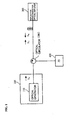
- Fig. 1 is a mimetic diagram illustrating a conventional optical communication system using an optical modulator having polarization dependency. Since a reflective semiconductor optical amplifier is usefully applied in a Wavelength Division Multiplexer-Passive Optical Network (hereinafter, referred to as "WDM-PON") as disclosed in "Semiconductor Laser Amplifier-Reflector for the Future FTTH Applications” (Vol. 2, p. 196) written by N. Buldawwo, S. Mottet, F. le Gall, D. Siggogne, D. Meichenin, S. Chelle in European Conference on Optical Communication, an example where the reflective semiconductor optical amplifier is used as an optical modulator having polarization dependency.
- WDM-PON Wavelength Division Multiplexer-Passive Optical Network
- the optical communication system comprises a light source 100, an optical circulator 200, a reflective semiconductor optical amplifier 300 and a photodiode 400.
- An optical generator 110 in the light source 100 outputs a continuous wave (hereinafter, abbreviated as "CW") laser light ⁇ s having a predetermined strength
- the representative example of the optical generator 110 is a Distributed Feedback Laser Diode (hereinafter, referred to as "DFB-LD").
- the laser light ⁇ s from the optical generator 110 is projected into the reflective semiconductor optical amplifier 300 through the optical circulator.
- the reflective semiconductor optical amplifier 300 receives the laser light ⁇ s to generate a modulated optical signal ⁇ m that has the same wavelength as that of the projected laser light ⁇ s .
- the optical signal ⁇ m modulated by the semiconductor optical amplifier 300 is inputted in the photodiode 400 through the optical circulator 200, and then transformed into an electric signal.
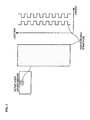
- Fig. 2 is a diagram illustrating the operation principle of the reflective semiconductor optical amplifier 300 of Fig. 1.
- the projected light ⁇ s inputted through the optical waveguide 310 is transmitted into the active layer waveguide 320, reflected in the high reflection coating film 330, and outputted to the optical waveguide 310 again.
- the projected light ⁇ s is processed along the active waveguide 330, the projected light ⁇ s is amplified depending on inputted signal current. Since a reflected output light copies the signal current, the reflective semiconductor optical amplifier 300 converts the light ⁇ s into the upstream optical signal ⁇ m having the same wavelength as that of the light ⁇ s .
- the active layer waveguide 320 has a quantum well structure which is formed of alternately deposited materials having a large energy band gap and a small energy band gap at tens of ⁇ .
- the state available in a Momentum space is two-dimensionally distributed, and the state depending on energy levels is intensively distributed in a specific energy level to increase photoelectric conversion efficiency.
- a quantum well layer has its horizontal structure different from its vertical structure, the distribution in the momentum direction of excited electrons is directional.
- a light projected into the semiconductor optical amplifier having a quantum well structure has different photoelectric conversion efficiency depending on its polarization direction. That is, in general, optical amplification gain by the semiconductor optical amplifier having a quantum well depends largely on the polarization direction of the projected light.
- the optical amplification gain is 20dB when the projected light is vertically polarized while the optical amplification gain is 10dB when the projected light is horizontally polarized.
- the laser light ⁇ s generated from the optical generator 110 by duplicating photons has polarization because a polarization characteristic is also duplicated during the above generation process.
- a single mode laser light having the polarization is used in an optical communication network, its polarization direction can be polarized due to distortion of an optical fiber.
- the modulated optical signal has a difference of the optical amplification gain as described above, which causes instability of the optical transmission system.
- an optical communication system comprising: a first optical generator and a second optical generator for generating a first single mode light and a second single mode light, respectively, wherein the first single mode light and the second single mode light are orthogonal and non-interfering with each other, and have the same wavelength; a mixing means for mixing the first single mode light and the second single mode light to output an orthogonal mode light; and an optical modulator for amplifying and modulating the orthogonal mode light after receiving the orthogonal mode light through an optical fiber so as to produce a constantly amplified optical signal regardless of a deflection degree of the orthogonal mode light.
- an optical communication method comprising: a first step of generating a first single mode light and a second single mode light, wherein the first single mode light and the second single mode light are orthogonal and non-interfering with each other, and have the same wavelength; a second step of mixing the first single mode light and the second single mode light to generate an orthogonal mode light; and a third step of receiving the orthogonal mode light through an optical fiber, and amplifying and modulating the received orthogonal mode light regardless of a deflection degree of the orthogonal mode light to produce a constantly amplified optical signal.
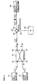
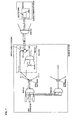
- Fig. 5 is a diagram illustrating an optical communication system according to a first embodiment of the present invention.
- the optical communication system of Fig. 5 is an example obtained by improving the structure of the light source 100 in the common optical communication system of Fig. 1.
- the detailed explanation on the elements such as the optical circulator 200, the reflective semiconductor optical amplifier 300 and the photodiode 400 in the common optical communication system is omitted.
- a light source 100 comprises optical generators 111 and 112, and a 3dB coupler 120.
- the first optical generator 111 generates a first single mode laser light ⁇ v,s polarized in a vertical direction through the above-described photon duplication process.
- the second optical generator 112 generates a second single laser light ⁇ h,s polarized in a horizontal direction.
- the two laser lights ⁇ v,s and ⁇ h,s are orthogonal and non-interfering with each other, and have the same wavelength.
- the orthogonal laser lights ⁇ v,s and ⁇ h,s are transmitted into two input terminals 121 and 122, and then branched into two output terminals 123 and 124 in the 3dB coupler 120, so that the laser lights ⁇ v,s and ⁇ h,s has a half power, respectively.
- the first single mode laser light ⁇ v,s and the second single laser light ⁇ h,s that are outputted from the output terminal 123 of the coupler 120 are mixed while they do not interfere each other, so that an orthogonal mode laser light ⁇ v+h,s is generated.
- the light for the orthogonal mode upstream signal can secure stability of the signal even when the light is modulated and amplified by a reflective semiconductor optical amplifier having polarization dependency. More specifically, the orthogonal mode laser light ⁇ v+h,s is transmitted into a first port 210 of an optical circulator 200. Then, the orthogonal mode laser light ⁇ v+h,s is outputted to a second port 202, and transmitted through an optical fiber into a reflective semiconductor optical amplifier.
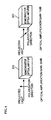
- the orthogonal mode laser light ⁇ v+h,s which is transmitted through the optical fiber is deflected by ⁇ rad. shown in Fig. 6 depending on the state of the optical fiber as described above.
- the deflected the orthogonal mode laser light ⁇ v+h,s is transmitted into the reflective semiconductor optical amplifier 300 to be modulated.
- the non-uniformity of the optical amplification gain shown in the prior art is not generated even when the optical signal modulated through the reflective semiconductor optical amplifier having polarization dependency is generated.
- the semiconductor optical amplifier 300 of Fig. 5 has the characteristic of Fig. 4, the powers of the single mode laser light ⁇ v,s arid ⁇ h,s are P, an optical fiber loss is L dB, and the optical fiber has no polarization dependency. If the polarization direction of the orthogonal mode laser light ⁇ v+h,s for an upstream signal is maintained, the power where the light polarized in the vertical and horizontal directions is projected into the optical amplifier 300 is P/2 ⁇ 10 -L/10 , and its electromagnetic strength is (P/2 ⁇ 10 -L/10 ) 1/2 .
- an optical power gain of the vertical polarization is 20dB, and a strength gain of an electromagnetic wave is 10dB. Therefore, the strength of the optical wave where a vertical element of the orthogonal mode laser light ⁇ v+h,s for an upstream signal is modulated in the optical amplifier 300 is (P/2 ⁇ 10 -L/10 ) 1/2 ⁇ 10 10/10 that is reduced by an optical power to obtain P/2 ⁇ 10 -L/10 ⁇ 10 20/10 .
- An optical power gain of the horizontal polarization is 10dB, and a strength gain of an electromagnetic wave is 5dB.
- the optical power where a horizontal element of the orthogonal mode laser light ⁇ v+h,s for an upstream signal is modulated in the optical amplifier 300 is P/2 ⁇ 10 -L/10.
- the optical power of the modulated optical signal can be obtained as follows. Since the electromagnetic strength of the vertical element of the projected light ⁇ v+h,s that is not deflected is (P/2 ⁇ 10 -L/10 ) 1/2 , the electromagnetic strength of the vertical element of ⁇ v,s of the projected lights in Fig. 6 is (P/2 ⁇ 10 -L/10 ) 1/2 ⁇ cos ⁇ and the electromagnetic strength of the horizontal element is (P/2 ⁇ 10 -L/10 ) 1/2. sin ⁇ .
- the electromagnetic strength of the horizontal element of ⁇ h,s of the projected lights in Fig. 6 is (P/2 ⁇ 10 -L/10 ) 1/2. cos ⁇ and the electromagnetic strength of the horizontal element is (P/2 ⁇ 10- L/10 ) 1/2. sin ⁇ .
- the optical power gain of the vertical element is 20dB and the optical power gain of the horizontal element is 10dB, the amplified optical power of the whole vertical elements of the projected light ⁇ v+h,s of Fig.
- the modulated optical signal has a predetermined optical power even when the projected light is deflected by a random angle and projected into the optical amplifier.
- the optical transmission system has a predetermined optical power gain regardless of polarization directions even when a reflective semiconductor optical amplifier having large polarization dependency is used.
- Fig 7 is a diagram illustrating an example where the first embodiment is applied in the WDM-PON.
- the two single mode laser lights that are orthogonal with each other having the same wavelength are inputted respectively into two input terminals of a 3dB coupler, mixed as an orthogonal mode laser light having a half power, and then outputted into two output terminals of the 3dB coupler.
- the orthogonal mode laser light which is used as a light for an upstream signal, is wavelength-division-multiplexed through two WDM 510 and 520, and then transmitted into a subscriber's station.
- the orthogonal mode laser light ⁇ i,v+h,s generated from the light source 100 is wavelength-division-multiplexed in the WDM 500 with a light having a different wavelength which is generated for other subscribers. Thereafter, the wavelength-division-multiplexed light ⁇ ⁇ i,v+h,s is split by a 1 x n optical splitter.
- the split light ⁇ ⁇ i,v+h,s for an upstream signal is transmitted into the j th one of a plurality of Optical Line Terminals (hereinafter, referred to as "OLT") in a base station.
- OLT Optical Line Terminal
- the split light ⁇ ⁇ i,v+h,s for an upstream signal is transmitted into the WDM 530 at the subscriber's side through the first port 201 and the second port 202 in the optical circulator 200 so that lights may be separated in each subscriber, and transmitted into an Optical Network Unit (hereinafter, referred to as "ONU") 700 of the i th subscriber.
- ONU Optical Network Unit
- the light ⁇ ⁇ i,v+h,s for an upstream signal is projected into the reflective semiconductor optical amplifier 300 in the ONU 700.
- An upstream optical signal ⁇ i,v+h,m generated from the reflective semiconductor optical amplifier 300 is transmitted into the WDM 530 through the optical fiber where the light ⁇ i,v+h,s for an upstream signal is transmitted, wavelength-division-multiplexed with upstream optical signals of other subscribers by the WDM 530, and then transmitted into an OLT 800 of the base station.
- the wavelength-division-multiplexed upstream optical signal ⁇ ⁇ i,s+h,m is projected into the second port 202 of the optical circulator 200 in the OLT 800, and then outputted into a third port 203.
- the optical signal ⁇ ⁇ i,v+h,m is transmitted into the photodiode 400 and converted into an electric signal.
- Fig. 8 is a diagram illustrating an optical communication system according to a second embodiment of the present invention.
- the light source 100 also comprises optical generators 111 and 112 like in the first embodiment, and single mode laser lights that are orthogonal with each other are generated.
- the single mode laser lights ⁇ v,s and ⁇ h,s are inputted in output terminals 141 and 142 of a Polarization Beam Splitter (hereinafter, referred to as "PBS") 130, and outputted to an input terminal of the PBS 130.
- PBS Polarization Beam Splitter
- a light ⁇ v+h,s is obtained by mixing lights ⁇ v,s and ⁇ h,s which have initial optical powers.
- the second embodiment can be used in the same optical communication network such as the WDM-PON like the first embodiment.
- an optical modulator having polarization dependency like a reflective semiconductor optical amplifier in an optical transmission network is used, a constantly amplified optical signal can be obtained regardless of deflection of a light inputted in the optical modulator, which results in stable optical transmission.
Landscapes
- Health & Medical Sciences (AREA)
- Engineering & Computer Science (AREA)
- Life Sciences & Earth Sciences (AREA)
- Biomedical Technology (AREA)
- Animal Behavior & Ethology (AREA)
- General Health & Medical Sciences (AREA)
- Public Health (AREA)
- Veterinary Medicine (AREA)
- Radiology & Medical Imaging (AREA)
- Nuclear Medicine, Radiotherapy & Molecular Imaging (AREA)
- Heart & Thoracic Surgery (AREA)
- Biophysics (AREA)
- Physics & Mathematics (AREA)
- Electromagnetism (AREA)
- Computer Networks & Wireless Communication (AREA)
- Signal Processing (AREA)
- Vascular Medicine (AREA)
- Optical Communication System (AREA)
- Optical Modulation, Optical Deflection, Nonlinear Optics, Optical Demodulation, Optical Logic Elements (AREA)
Abstract
Description
Claims (6)
- An optical communication system comprising:a first optical generator and a second optical generator for generating a first single mode light and a second single mode light, respectively, wherein the first single mode light and the second single mode light are orthogonal and non-interfering with each other, and have the same wavelength;a mixing means for mixing the first single mode light and the second single mode light to output an orthogonal mode light; andan optical modulator for amplifying and modulating the orthogonal mode light after receiving the orthogonal mode light through an optical fiber so as to produce a constantly amplified optical signal regardless of a deflection degree of the orthogonal mode light.
- The optical communication system according to claim 1, wherein the mixing means is a 3dB coupler.
- The optical communication system according to claim 1, wherein the mixing means is a polarization beam splitter.
- An optical communication method comprising:a first step of generating a first single mode light and a second single mode light, wherein the first single mode light and the second single mode light are orthogonal and non-interfering with each other, and have the same wavelength;a second step of mixing the first single mode light and the second single mode light to generate an orthogonal mode light; anda third step of receiving the orthogonal mode light through an optical fiber, and amplifying and modulating the received orthogonal mode light regardless of a deflection degree of the orthogonal mode light to produce a constantly amplified optical signal.
- The optical communication method according to claim 4, wherein the second step is performed by using a 3dB coupler.
- The optical communication method according to claim 4, wherein the second step is performed by using a polarization beam splitter.
Applications Claiming Priority (2)
| Application Number | Priority Date | Filing Date | Title |
|---|---|---|---|
| KR2004007148 | 2004-02-04 | ||
| KR1020040007148A KR100945137B1 (en) | 2004-02-04 | 2004-02-04 | Optical communication system and method |
Publications (3)
| Publication Number | Publication Date |
|---|---|
| EP1562311A2 true EP1562311A2 (en) | 2005-08-10 |
| EP1562311A3 EP1562311A3 (en) | 2006-05-24 |
| EP1562311B1 EP1562311B1 (en) | 2008-10-29 |
Family
ID=34675998
Family Applications (1)
| Application Number | Title | Priority Date | Filing Date |
|---|---|---|---|
| EP05250582A Expired - Lifetime EP1562311B1 (en) | 2004-02-04 | 2005-02-03 | Optical communication system and method thereof |
Country Status (7)
| Country | Link |
|---|---|
| US (1) | US7197206B2 (en) |
| EP (1) | EP1562311B1 (en) |
| JP (1) | JP4276188B2 (en) |
| KR (1) | KR100945137B1 (en) |
| CN (1) | CN1318870C (en) |
| AT (1) | ATE413026T1 (en) |
| DE (1) | DE602005010620D1 (en) |
Families Citing this family (7)
| Publication number | Priority date | Publication date | Assignee | Title |
|---|---|---|---|---|
| US7738167B2 (en) * | 2005-12-09 | 2010-06-15 | Electronics And Telecommunications Research Institute | Reflective semiconductor optical amplifier (RSOA), RSOA module having the same, and passive optical network using the same |
| KR100819034B1 (en) * | 2006-05-11 | 2008-04-03 | 한국전자통신연구원 | Passive optical networkPON based on reflective semiconductor optical amplifierRSOA |
| CN102082610B (en) * | 2009-12-01 | 2014-07-30 | 华为技术有限公司 | Self-injection locking light source and light source self-injection locking method and system |
| DE112011101260T5 (en) | 2010-04-09 | 2013-05-02 | Semiconductor Energy Laboratory Co., Ltd. | A liquid crystal display device and method for driving the same |
| CN104716561A (en) * | 2013-12-12 | 2015-06-17 | 青岛海信宽带多媒体技术有限公司 | Laser |
| US10153849B2 (en) * | 2013-12-24 | 2018-12-11 | Telefonaktiebolaget Lm Ericsson (Publ) | FSO communications terminals for connecting telecommunications cards |
| CN113014231B (en) * | 2021-03-05 | 2023-12-19 | 南京晓庄学院 | Three pairs of parameter-adjustable and controllable photoelectric delay positive feedback laser broadband signal dual generators |
Family Cites Families (5)
| Publication number | Priority date | Publication date | Assignee | Title |
|---|---|---|---|---|
| JPH0727149B2 (en) * | 1986-11-04 | 1995-03-29 | 沖電気工業株式会社 | Optical coupler |
| NL9101244A (en) | 1991-07-15 | 1993-02-01 | Nederland Ptt | POLARIZATION-SENSITIVE GAINING DEVICE. |
| JP3284507B2 (en) | 1993-06-28 | 2002-05-20 | 富士通株式会社 | Optical transmitting device and optical amplifying device for optical communication system |
| EP1128503A3 (en) * | 2000-02-28 | 2003-08-06 | Nortel Networks Limited | Optical amplifier stage |
| US6522796B1 (en) * | 2000-10-24 | 2003-02-18 | Jds Uniphase Corporation | Depolarizing polarization mode combiner |
-
2004
- 2004-02-04 KR KR1020040007148A patent/KR100945137B1/en not_active Expired - Lifetime
-
2005
- 2005-02-02 US US11/048,972 patent/US7197206B2/en not_active Expired - Lifetime
- 2005-02-03 AT AT05250582T patent/ATE413026T1/en not_active IP Right Cessation
- 2005-02-03 DE DE602005010620T patent/DE602005010620D1/en not_active Expired - Fee Related
- 2005-02-03 EP EP05250582A patent/EP1562311B1/en not_active Expired - Lifetime
- 2005-02-04 CN CNB2005100091088A patent/CN1318870C/en not_active Expired - Fee Related
- 2005-02-04 JP JP2005029012A patent/JP4276188B2/en not_active Expired - Fee Related
Also Published As
| Publication number | Publication date |
|---|---|
| KR20050079053A (en) | 2005-08-09 |
| JP4276188B2 (en) | 2009-06-10 |
| US7197206B2 (en) | 2007-03-27 |
| EP1562311B1 (en) | 2008-10-29 |
| CN1651946A (en) | 2005-08-10 |
| KR100945137B1 (en) | 2010-03-02 |
| DE602005010620D1 (en) | 2008-12-11 |
| ATE413026T1 (en) | 2008-11-15 |
| CN1318870C (en) | 2007-05-30 |
| EP1562311A3 (en) | 2006-05-24 |
| US20050169574A1 (en) | 2005-08-04 |
| JP2005223923A (en) | 2005-08-18 |
Similar Documents
| Publication | Publication Date | Title |
|---|---|---|
| US12107628B2 (en) | Systems and methods for full duplex coherent optics | |
| Hofstetter et al. | Dispersion effects in optical millimeter-wave systems using self-heterodyne method for transport and generation | |
| CN110868258B (en) | Device, system and method for realizing coherent detection | |
| US6067187A (en) | Optical amplifier and optical communication system employing the same | |
| US7474460B2 (en) | Optical modulation apparatus | |
| JP3154418B2 (en) | Semiconductor optical amplifier, optical communication system, bidirectional optical communication system, optical communication network, and integrated optical node | |
| JPH08251109A (en) | Self-amplifying network | |
| US10355452B2 (en) | Optical module and method for controlling optical module | |
| US7197206B2 (en) | Optical communication system and method thereof | |
| JP3625932B2 (en) | Wavelength converter | |
| US5436751A (en) | Analog optical transmission system and optical fiber amplifier | |
| US20050157378A1 (en) | Reduced four-wave mixing and raman amplification architecture | |
| US6909534B2 (en) | Wideband four-wave-mixing wavelength converter | |
| US8509627B2 (en) | Reflective optical transmitter | |
| CN118199735A (en) | Optical transmission method and device based on semiconductor optical amplifier | |
| US7016614B1 (en) | Optical wavelength division multiplexing transmission suppressing four-wave mixing and SPM-GVD effects | |
| CN110456453A (en) | Optical communication device, optical communication method, and computer-readable medium | |
| WO2023160774A1 (en) | Dummy light module comprising dual semiconductor optical amplifier | |
| EP1306989B1 (en) | Lossless optical splitter | |
| Suzuki et al. | Coherent Beam Combining System with Pseudorandom Optical Phase Modulation for Realizing High-Power Laser System | |
| Schares et al. | Multi-wavelength mixing in a semiconductor optical amplifier and its consequence in a preamplified wavelength division multiplexing system | |
| US20060152798A1 (en) | Non-inverting cross-gain modulation-based wavelength converter | |
| JPH0964437A (en) | Rare-earth element-doped optical fiber amplifier | |
| JP3388956B2 (en) | Optical transmission equipment | |
| TW588166B (en) | Coherent power combining of single-mode sources in waveguide fiber couplers |
Legal Events
| Date | Code | Title | Description |
|---|---|---|---|
| PUAI | Public reference made under article 153(3) epc to a published international application that has entered the european phase |
Free format text: ORIGINAL CODE: 0009012 |
|
| 17P | Request for examination filed |
Effective date: 20050218 |
|
| AK | Designated contracting states |
Kind code of ref document: A2 Designated state(s): AT BE BG CH CY CZ DE DK EE ES FI FR GB GR HU IE IS IT LI LT LU MC NL PL PT RO SE SI SK TR |
|
| AX | Request for extension of the european patent |
Extension state: AL BA HR LV MK YU |
|
| PUAL | Search report despatched |
Free format text: ORIGINAL CODE: 0009013 |
|
| AK | Designated contracting states |
Kind code of ref document: A3 Designated state(s): AT BE BG CH CY CZ DE DK EE ES FI FR GB GR HU IE IS IT LI LT LU MC NL PL PT RO SE SI SK TR |
|
| AX | Request for extension of the european patent |
Extension state: AL BA HR LV MK YU |
|
| AKX | Designation fees paid |
Designated state(s): AT BE BG CH CY CZ DE DK EE ES FI FR GB GR HU IE IS IT LI LT LU MC NL PL PT RO SE SI SK TR |
|
| 17Q | First examination report despatched |
Effective date: 20070227 |
|
| GRAP | Despatch of communication of intention to grant a patent |
Free format text: ORIGINAL CODE: EPIDOSNIGR1 |
|
| GRAS | Grant fee paid |
Free format text: ORIGINAL CODE: EPIDOSNIGR3 |
|
| GRAA | (expected) grant |
Free format text: ORIGINAL CODE: 0009210 |
|
| AK | Designated contracting states |
Kind code of ref document: B1 Designated state(s): AT BE BG CH CY CZ DE DK EE ES FI FR GB GR HU IE IS IT LI LT LU MC NL PL PT RO SE SI SK TR |
|
| REG | Reference to a national code |
Ref country code: GB Ref legal event code: FG4D |
|
| REG | Reference to a national code |
Ref country code: CH Ref legal event code: EP |
|
| REG | Reference to a national code |
Ref country code: IE Ref legal event code: FG4D |
|
| REF | Corresponds to: |
Ref document number: 602005010620 Country of ref document: DE Date of ref document: 20081211 Kind code of ref document: P |
|
| NLV1 | Nl: lapsed or annulled due to failure to fulfill the requirements of art. 29p and 29m of the patents act | ||
| LTIE | Lt: invalidation of european patent or patent extension |
Effective date: 20081029 |
|
| PG25 | Lapsed in a contracting state [announced via postgrant information from national office to epo] |
Ref country code: AT Free format text: LAPSE BECAUSE OF FAILURE TO SUBMIT A TRANSLATION OF THE DESCRIPTION OR TO PAY THE FEE WITHIN THE PRESCRIBED TIME-LIMIT Effective date: 20081029 Ref country code: BG Free format text: LAPSE BECAUSE OF FAILURE TO SUBMIT A TRANSLATION OF THE DESCRIPTION OR TO PAY THE FEE WITHIN THE PRESCRIBED TIME-LIMIT Effective date: 20090129 Ref country code: ES Free format text: LAPSE BECAUSE OF FAILURE TO SUBMIT A TRANSLATION OF THE DESCRIPTION OR TO PAY THE FEE WITHIN THE PRESCRIBED TIME-LIMIT Effective date: 20090209 Ref country code: LT Free format text: LAPSE BECAUSE OF FAILURE TO SUBMIT A TRANSLATION OF THE DESCRIPTION OR TO PAY THE FEE WITHIN THE PRESCRIBED TIME-LIMIT Effective date: 20081029 |
|
| PG25 | Lapsed in a contracting state [announced via postgrant information from national office to epo] |
Ref country code: NL Free format text: LAPSE BECAUSE OF FAILURE TO SUBMIT A TRANSLATION OF THE DESCRIPTION OR TO PAY THE FEE WITHIN THE PRESCRIBED TIME-LIMIT Effective date: 20081029 Ref country code: FI Free format text: LAPSE BECAUSE OF FAILURE TO SUBMIT A TRANSLATION OF THE DESCRIPTION OR TO PAY THE FEE WITHIN THE PRESCRIBED TIME-LIMIT Effective date: 20081029 Ref country code: PT Free format text: LAPSE BECAUSE OF FAILURE TO SUBMIT A TRANSLATION OF THE DESCRIPTION OR TO PAY THE FEE WITHIN THE PRESCRIBED TIME-LIMIT Effective date: 20090330 Ref country code: PL Free format text: LAPSE BECAUSE OF FAILURE TO SUBMIT A TRANSLATION OF THE DESCRIPTION OR TO PAY THE FEE WITHIN THE PRESCRIBED TIME-LIMIT Effective date: 20081029 Ref country code: IS Free format text: LAPSE BECAUSE OF FAILURE TO SUBMIT A TRANSLATION OF THE DESCRIPTION OR TO PAY THE FEE WITHIN THE PRESCRIBED TIME-LIMIT Effective date: 20090228 Ref country code: SI Free format text: LAPSE BECAUSE OF FAILURE TO SUBMIT A TRANSLATION OF THE DESCRIPTION OR TO PAY THE FEE WITHIN THE PRESCRIBED TIME-LIMIT Effective date: 20081029 |
|
| PG25 | Lapsed in a contracting state [announced via postgrant information from national office to epo] |
Ref country code: BE Free format text: LAPSE BECAUSE OF FAILURE TO SUBMIT A TRANSLATION OF THE DESCRIPTION OR TO PAY THE FEE WITHIN THE PRESCRIBED TIME-LIMIT Effective date: 20081029 Ref country code: EE Free format text: LAPSE BECAUSE OF FAILURE TO SUBMIT A TRANSLATION OF THE DESCRIPTION OR TO PAY THE FEE WITHIN THE PRESCRIBED TIME-LIMIT Effective date: 20081029 Ref country code: DK Free format text: LAPSE BECAUSE OF FAILURE TO SUBMIT A TRANSLATION OF THE DESCRIPTION OR TO PAY THE FEE WITHIN THE PRESCRIBED TIME-LIMIT Effective date: 20081029 Ref country code: RO Free format text: LAPSE BECAUSE OF FAILURE TO SUBMIT A TRANSLATION OF THE DESCRIPTION OR TO PAY THE FEE WITHIN THE PRESCRIBED TIME-LIMIT Effective date: 20081029 |
|
| PG25 | Lapsed in a contracting state [announced via postgrant information from national office to epo] |
Ref country code: CZ Free format text: LAPSE BECAUSE OF FAILURE TO SUBMIT A TRANSLATION OF THE DESCRIPTION OR TO PAY THE FEE WITHIN THE PRESCRIBED TIME-LIMIT Effective date: 20081029 Ref country code: SE Free format text: LAPSE BECAUSE OF FAILURE TO SUBMIT A TRANSLATION OF THE DESCRIPTION OR TO PAY THE FEE WITHIN THE PRESCRIBED TIME-LIMIT Effective date: 20090129 Ref country code: IT Free format text: LAPSE BECAUSE OF FAILURE TO SUBMIT A TRANSLATION OF THE DESCRIPTION OR TO PAY THE FEE WITHIN THE PRESCRIBED TIME-LIMIT Effective date: 20081029 |
|
| PLBE | No opposition filed within time limit |
Free format text: ORIGINAL CODE: 0009261 |
|
| STAA | Information on the status of an ep patent application or granted ep patent |
Free format text: STATUS: NO OPPOSITION FILED WITHIN TIME LIMIT |
|
| PG25 | Lapsed in a contracting state [announced via postgrant information from national office to epo] |
Ref country code: MC Free format text: LAPSE BECAUSE OF NON-PAYMENT OF DUE FEES Effective date: 20090228 Ref country code: SK Free format text: LAPSE BECAUSE OF FAILURE TO SUBMIT A TRANSLATION OF THE DESCRIPTION OR TO PAY THE FEE WITHIN THE PRESCRIBED TIME-LIMIT Effective date: 20081029 |
|
| REG | Reference to a national code |
Ref country code: CH Ref legal event code: PL |
|
| 26N | No opposition filed |
Effective date: 20090730 |
|
| PG25 | Lapsed in a contracting state [announced via postgrant information from national office to epo] |
Ref country code: CH Free format text: LAPSE BECAUSE OF NON-PAYMENT OF DUE FEES Effective date: 20090228 Ref country code: LI Free format text: LAPSE BECAUSE OF NON-PAYMENT OF DUE FEES Effective date: 20090228 |
|
| REG | Reference to a national code |
Ref country code: IE Ref legal event code: MM4A |
|
| REG | Reference to a national code |
Ref country code: FR Ref legal event code: ST Effective date: 20091030 |
|
| PG25 | Lapsed in a contracting state [announced via postgrant information from national office to epo] |
Ref country code: DE Free format text: LAPSE BECAUSE OF NON-PAYMENT OF DUE FEES Effective date: 20090901 Ref country code: IE Free format text: LAPSE BECAUSE OF NON-PAYMENT OF DUE FEES Effective date: 20090203 |
|
| PG25 | Lapsed in a contracting state [announced via postgrant information from national office to epo] |
Ref country code: FR Free format text: LAPSE BECAUSE OF NON-PAYMENT OF DUE FEES Effective date: 20090302 |
|
| PG25 | Lapsed in a contracting state [announced via postgrant information from national office to epo] |
Ref country code: GR Free format text: LAPSE BECAUSE OF FAILURE TO SUBMIT A TRANSLATION OF THE DESCRIPTION OR TO PAY THE FEE WITHIN THE PRESCRIBED TIME-LIMIT Effective date: 20090130 |
|
| PG25 | Lapsed in a contracting state [announced via postgrant information from national office to epo] |
Ref country code: LU Free format text: LAPSE BECAUSE OF NON-PAYMENT OF DUE FEES Effective date: 20090203 |
|
| PG25 | Lapsed in a contracting state [announced via postgrant information from national office to epo] |
Ref country code: HU Free format text: LAPSE BECAUSE OF FAILURE TO SUBMIT A TRANSLATION OF THE DESCRIPTION OR TO PAY THE FEE WITHIN THE PRESCRIBED TIME-LIMIT Effective date: 20090430 |
|
| PG25 | Lapsed in a contracting state [announced via postgrant information from national office to epo] |
Ref country code: TR Free format text: LAPSE BECAUSE OF FAILURE TO SUBMIT A TRANSLATION OF THE DESCRIPTION OR TO PAY THE FEE WITHIN THE PRESCRIBED TIME-LIMIT Effective date: 20081029 |
|
| PG25 | Lapsed in a contracting state [announced via postgrant information from national office to epo] |
Ref country code: CY Free format text: LAPSE BECAUSE OF FAILURE TO SUBMIT A TRANSLATION OF THE DESCRIPTION OR TO PAY THE FEE WITHIN THE PRESCRIBED TIME-LIMIT Effective date: 20081029 |
|
| PGFP | Annual fee paid to national office [announced via postgrant information from national office to epo] |
Ref country code: GB Payment date: 20150218 Year of fee payment: 11 |
|
| GBPC | Gb: european patent ceased through non-payment of renewal fee |
Effective date: 20160203 |
|
| PG25 | Lapsed in a contracting state [announced via postgrant information from national office to epo] |
Ref country code: GB Free format text: LAPSE BECAUSE OF NON-PAYMENT OF DUE FEES Effective date: 20160203 |