EP1560193A1 - Organic electroluminescent display device - Google Patents
Organic electroluminescent display device Download PDFInfo
- Publication number
- EP1560193A1 EP1560193A1 EP04078425A EP04078425A EP1560193A1 EP 1560193 A1 EP1560193 A1 EP 1560193A1 EP 04078425 A EP04078425 A EP 04078425A EP 04078425 A EP04078425 A EP 04078425A EP 1560193 A1 EP1560193 A1 EP 1560193A1
- Authority
- EP
- European Patent Office
- Prior art keywords
- electrode
- power line
- electro luminescence
- organic electro
- luminescence display
- Prior art date
- Legal status (The legal status is an assumption and is not a legal conclusion. Google has not performed a legal analysis and makes no representation as to the accuracy of the status listed.)
- Granted
Links
Images




Classifications
-
- H—ELECTRICITY
- H10—SEMICONDUCTOR DEVICES; ELECTRIC SOLID-STATE DEVICES NOT OTHERWISE PROVIDED FOR
- H10K—ORGANIC ELECTRIC SOLID-STATE DEVICES
- H10K59/00—Integrated devices, or assemblies of multiple devices, comprising at least one organic light-emitting element covered by group H10K50/00
- H10K59/10—OLED displays
- H10K59/12—Active-matrix OLED [AMOLED] displays
- H10K59/131—Interconnections, e.g. wiring lines or terminals
- H10K59/1315—Interconnections, e.g. wiring lines or terminals comprising structures specially adapted for lowering the resistance
-
- H—ELECTRICITY
- H05—ELECTRIC TECHNIQUES NOT OTHERWISE PROVIDED FOR
- H05B—ELECTRIC HEATING; ELECTRIC LIGHT SOURCES NOT OTHERWISE PROVIDED FOR; CIRCUIT ARRANGEMENTS FOR ELECTRIC LIGHT SOURCES, IN GENERAL
- H05B33/00—Electroluminescent light sources
- H05B33/12—Light sources with substantially two-dimensional [2D] radiating surfaces
- H05B33/26—Light sources with substantially two-dimensional [2D] radiating surfaces characterised by the composition or arrangement of the conductive material used as an electrode
-
- H—ELECTRICITY
- H10—SEMICONDUCTOR DEVICES; ELECTRIC SOLID-STATE DEVICES NOT OTHERWISE PROVIDED FOR
- H10K—ORGANIC ELECTRIC SOLID-STATE DEVICES
- H10K2102/00—Constructional details relating to the organic devices covered by this subclass
- H10K2102/301—Details of OLEDs
- H10K2102/302—Details of OLEDs of OLED structures
- H10K2102/3023—Direction of light emission
- H10K2102/3026—Top emission
Definitions
- the present invention relates to an organic electro luminescence display and, more particularly, to an organic electro luminescence display in which a cathode power line is connected with a cathode electrode by a plurality of contact holes.
- organic electro luminescence displays are self-emissive displays that are classified, according to the direction of light emitted from their organic emission layer, as either bottom-emitting types, top-emitting types, or dual-emitting types.
- the top-emitting type emits light in a direction away from the substrate on which the pixels are arranged, while the bottom-emitting type emits light toward the substrate on which the pixels are arranged.
- Top-emitting types have a higher aperture ratio than bottom-emitting types.
- the transparent electrode is made of transparent conductive material such as Indium Tin Oxide (ITO).
- ITO Indium Tin Oxide
- Transparent conductive material has a high resistance value, however, which causes a voltage (IR) drop, thereby creating an inconsistent brightness on the display.
- a technology has been proposed that uses a metallic material as a cathode power line for supplying a cathode voltage to a transparent cathode electrode, which is one of the two electrodes formed on the upper and lower portions of the organic emission layer.
- FIG. 1 shows a plan view of a conventional organic electro luminescence display with a cathode power line.
- a conventional organic electro luminescence display 100 comprises a pixel portion 110 on which a plurality of pixels are arranged, an upper power line 120 on the top, right and left sides of the pixel portion 110 to supply the power supply voltage VDD, a lower power line 130 on the bottom side of the pixel portion 110 to supply the power supply voltage VDD, a scan driver 140 that supplies a scan signal sequentially to pixels of the pixel portion 110, a data driver 150 that supplies a data signal to pixels of the pixel portion 110, and a cathode electrode 160, which is formed to cover all of the pixel portion 110.
- the conventional organic electro luminescence display 100 further comprises an external terminal 171, which is used to apply an external voltage to the cathode power line 170.
- the cathode power line 170 is connected with the cathode electrode 160 by contact hole 180, thereby connecting the cathode electrode 160 to the external voltage supplied at the external terminal 171.
- the scan driver 140 signal and the data driver 150 signal are transmitted to the pixels in the pixel portion 110.
- a predetermined level of power supply voltage VDD is supplied from the upper and lower power lines 120, 130 to the pixels in the pixel portion 110, and the cathode voltage is supplied from the cathode power line 170 to the cathode electrode 160 via the contact hole 180.
- Switching and driving transistors (not shown) provided in each of the pixels arranged in the pixel portion 110 then operate, so that light is emitted from the organic emission layer and transmitted through the cathode electrode 160.
- IR voltage
- the present invention is directed to an organic electro luminescence display that substantially obviates one or more of the problems due to limitations and disadvantages of the related art.
- the present invention provides an organic electro luminescence display in which current mobility is increased by connecting a cathode power line to a cathode electrode via a plurality of contact holes.
- the present invention also provides an organic electro luminescence display that can prevent a voltage (IR) drop in a cathode power by utilizing auxiliary cathode power lines to supply the external terminal voltage to the cathode power line.
- the present invention provides an organic electro luminescence display comprising a pixel portion on which a plurality of pixels are arranged with a first electrode, a second electrode, and an organic thin film layer interposed between the first and second electrodes; a first power line supplying a first level voltage to the pixels of the pixel portion; a second power line having at least a region overlapped with the second electrode to supply a second level voltage to the second electrode, an insulating layer having a plurality of contact holes in the overlapped region between the second power line and the second electrode; and the sum of circumferences of each contact hole is greater than the circumference of the overlapped region.
- the organic electro luminescence display may comprise an insulating layer having a plurality of contact holes in the overlapped region between the second power line and the second electrode, wherein the second power line is arranged in at least one side of the pixel portion, and wherein the second power line includes a plurality of auxiliary power lines for supplying the voltage to the second electrode.
- the organic electro luminescence display may well comprise an insulating layer having a plurality of contact holes in the overlapped region between the second power line and the second electrode, wherein the plurality of contact holes, arranged in rows and columns, allow the second electrode to be connected with the second power line, and wherein the insulating layer includes at least two contact holes in the column direction.
- FIG. 1 shows a plan view of a conventional organic electro luminescence display.
- FIG. 2 shows a plan view of the cathode power line connected with the cathode electrode by a contact hole in the conventional organic electro luminescence display of FIG. 1.
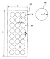
- FIG. 3 shows a plan view of a cathode power line connected with a cathode electrode by a plurality of contact holes in an organic electro luminescence display according to a first exemplary embodiment of the present invention.
- FIG. 4 shows a plan view of a cathode power line connected with a cathode electrode by a plurality of contact holes in an organic electro luminescence display according to a second exemplary embodiment of the present invention.
- FIG. 5 shows a plan view of a cathode power line connected with a cathode electrode by a plurality of contact holes in an organic electro luminescence display according to a third exemplary embodiment of the present invention.
- FIG. 6 shows a plan view of a cathode power line in an organic electro luminescence display according to a fourth exemplary embodiment of the present invention.
- FIG. 3 shows a plan view of a cathode power line connected with a cathode electrode by a plurality of contact holes in an organic electro luminescence display according to a first exemplary embodiment of the present invention. Since the first exemplary embodiment of the present invention is the same as the organic electro luminescence display illustrated in FIG. 1 except for the structure of the cathode power line and the contact holes, only the cathode power line and the contact holes are illustrated in FIG. 3.
- An organic electro luminescence display comprises a pixel portion on which a plurality of pixels are arranged; an upper power line on the top, right and left sides of the pixel portion to supply the power supply voltage VDD; a lower power line on the bottom side of the pixel portion to supply the power supply voltage VDD; a scan driver that supplies a scan signal sequentially to the pixels of the pixel portion; a data driver that supplies a data signal to the pixels of the pixel portion; a cathode electrode that is formed to cover all of the pixel portion; and a cathode power line that is overlapped with the cathode electrode and supplies a cathode voltage from an external terminal to the cathode electrode.
- the cathode power line 270 is electrically connected with the cathode electrode by a plurality of contact holes 280, which are formed in an interposed insulating layer (not shown).
- the contact holes 280 are arranged in a matrix comprised of rows and columns in the region where the cathode power line 270 is overlapped with the cathode electrode, so that each row and each column has the same number of contact holes. Further, all contact holes 280 are congruent, and they are arranged to have the same distance between each other in the row and column direction, although the distance between adjacent holes in the row direction need not be the same as the distance between adjacent holes in the column direction. According to the first exemplary embodiment of the present invention as shown in FIG. 3, the contact hole 280 has a square shape, but the contact hole 280 may have any other shape including rectangular, circular, elliptical, and polygonal.
- the total circumference of the plurality of contact holes 280 according to the first exemplary embodiment as shown in FIG. 3 is as determined below.
- each contact hole 280 Let the lengths of each contact hole 280 be "z” and “t”, in the row and column directions, respectively, and the distance between the adjacent contact holes 280 be “s” and “w”, in the row and column directions, respectively. Therefore, the area of each contact hole 280 is “z x t", and the circumference of each contact hole 280 is "2(z + t)". If “n” is the total number of contact holes 280 in the region where the cathode power line 270 is overlapped with the cathode electrode, then the total area of all contact holes 280 is "n(z ⁇ t )" and the total circumference of all contact holes 280 is "2n(z + t)".
- the voltage (IR) drop can be prevented by arranging the plurality of contact holes to satisfy the following two conditions: (1) L ⁇ A > n(z ⁇ t) (2) 2n(z ⁇ t) > 2(A + L)
- the distances "s" and “w” between each adjacent contact hole 280 should be less than or equal to either of the lengths "z” or “t” of each contact hole 280.
- the distances "s" and “w” between each adjacent contact hole 280 should be less than or equal to the least of "z” and "t”.
- the total circumference of the plurality of contact holes is greater than the circumference of the region where the cathode power line is overlapped with the cathode electrode, thereby increasing the current mobility and preventing the voltage (IR) drop.
- the center of each contact hole 280 is the point at which the current density is lowest.
- the plurality of contact holes are formed to have a total circumference greater than the circumference of the region where the cathode power line is overlapped with the cathode electrode, there are formed a plurality of regions having the high current density of an equivalent level along the equipotential lines in the edge of the each contact hole 280. This increases current mobility.
- a plurality of contact holes 280 formed within an organic electro luminescence display can reduce the voltage (IR) drop by increasing the current mobility, thereby preventing a decrease in the brightness of the display.
- FIG. 4 shows a plan view of a cathode power line connected with a cathode electrode by a plurality of contact holes in an organic electro luminescence display according to a second exemplary embodiment of the present invention. Since the second exemplary embodiment of the present invention is the same as the organic electro luminescence display illustrated in FIG. 1 except for the structure of the cathode power line and the contact holes, only the cathode power line and the contact holes are illustrated in FIG. 4.
- the cathode power line 270 is electrically coupled to the cathode electrode by a plurality of contact holes 280, which are formed in an interposed insulating layer (not shown).
- the contact holes 280 are arranged in a matrix comprised of rows and columns in the region where the cathode power line 270 is overlapped with the cathode electrode, so that each row and each column has the same number of contact holes. Further, all contact holes 280 are congruent, and they are arranged to have the same distance between each other in the row and column direction, although the distance between adjacent holes in the row and column direction need not be the same as the distance between adjacent holes in the column direction. According to the second exemplary embodiment of the present invention as shown in FIG. 4, the contact hole 280 has a circular shape, but the contact hole 280 may have any other shape including rectangular, square, elliptical, and polygonal.
- the total circumference of the plurality of contact holes 280 according to the second exemplary embodiment as shown in FIG.4 is as follows.
- each contact hole 280 Let the radius of each contact hole 280 be "r", and the distances between the adjacent contact holes 280 be “s” and “w” in the row and column directions, respectively. Therefore, the area of each contact hole 280 is “ ⁇ r 2 ", and the circumference of each contact hole 280 is “2 ⁇ r”. If “n” is the total number of contact holes 280 in the region where the cathode power line 270 is overlapped with the cathode electrode, then the total area of all contact holes 280 is "n ⁇ r 2 " and the total circumference of all contact holes 280 is "2n ⁇ r".
- the voltage (IR) drop can be prevented by arranging the plurality of contact holes to satisfy the following conditions (3) and (4).
- the distances "s" and “w” between each adjacent contact hole 280 should be less than or equal to the diameter (2r) of each contact hole 280.
- the total area of the plurality of contact holes is less than the area of the single contact hole of the conventional organic electro luminescence display, but the total circumference of the plurality of contact holes is greater than the circumference of the conventional single contact hole.
- the whole current mobility increases thereby decreasing the voltage (IR) drop, which prevents a decrease in the brightness of the display.
- FIG. 5 shows a plan view of a cathode power line connected with a cathode electrode by a plurality of contact holes in an organic electro luminescence display according to a third exemplary embodiment of the present invention. Since the third exemplary embodiment of the present invention is the same as the organic electro luminescence display illustrated in FIG. 1 except for the structure of the cathode power line and the contact holes, only the cathode power line and the contact holes are illustrated in FIG. 5.
- the cathode power line 270 is electrically coupled to the cathode electrode by a plurality of contact holes 280, which are formed in an interposed insulating layer (not shown).
- the contact holes 280 are arranged as a single column in the region where the cathode power line 270 is overlapped with the cathode electrode. Additionally, all contact holes 280 are congruent, and they are arranged to have the same distance between each adjacent contact hole 280. According to the third exemplary embodiment of the present invention as shown in FIG. 5, the contact hole 280 has a rectangular shape, but the contact hole 280 may have any other shape including circular, square, elliptical, and polygonal.
- the contact holes 280 are formed so that the foregoing conditions (1) and (2) are satisfied.
- the total circumference of the plurality of contact holes is greater than the circumference of the region of the cathode power line that is overlapped with the cathode electrode, thereby increasing the current mobility and preventing the voltage (IR) drop.
- the distance "w" between the adjacent contact holes arranged in a single column should be equal to or less than the lengths of each contact hole in the column direction.
- the exemplary embodiments shown in FIGs. 3, 4, and 5 show the contact holes in the insulating layer between the cathode power line and cathode electrode to be of the same size and shape, but they may be formed in different sizes and shapes. In other words, rectangular contact holes and circular contact holes may be formed together in the insulating layer. As with the exemplary embodiments shown in FIGs. 3, 4, and 5, however, the total circumference of the different sized and shaped contact holes must be greater than the circumference of the region where the cathode power line is overlapped the cathode electrode.
- FIG. 6 shows a plan view of an organic electro luminescence display according to a fourth exemplary embodiment of the present invention. Since the fourth exemplary embodiment of the present invention is the same as the organic electro luminescence display illustrated in FIG. 1 except for the structure of the cathode power line and the contact holes,, only a connection portion of the cathode power line is illustrated in FIG. 6. Contact holes are not illustrated in FIG. 6.
- the organic electro luminescence display according to a fourth embodiment of the present invention comprises a cathode power line 570 overlapped with, and supplying a cathode voltage to, a cathode electrode 560, and cathode auxiliary power lines 571, 572, 573, and 574 to supply the voltage applied at the external terminal 550 to the cathode power line 570.
- the cathode voltage When cathode voltage is applied at the external terminal 550, the cathode voltage is supplied to four sides of the cathode power line 570 through the cathode auxiliary power lines 571, 572, 573, and 574.
- the cathode voltage is, in turn, supplied from the cathode power line 570 to the cathode electrode 560 via a plurality of contact holes as exemplified in the first, second, and third exemplary embodiments.
- the cathode voltage is supplied from the external terminal 550 to four sides of the cathode power line 570 through the cathode auxiliary power lines 571, 572, 573, and 574.
- the cathode voltage is supplied from the external terminal to one side of the cathode power line.
- the cathode voltage is supplied from one external terminal 550 to four sides of the cathode power line 570 through the cathode auxiliary power lines 571, 572, 573, and 574, but it may also be supplied from a plurality of external terminals 550 to four sides of the cathode power line 570 through the cathode auxiliary power lines 571, 572, 573, and 574, respectively. Further, the cathode voltage may be supplied through the respective cathode auxiliary power lines to two or three sides, as well as four sides of the cathode power line.
- a plurality of cathode auxiliary lines may also be arranged on one, two, or three sides of the cathode power line, and thus the cathode voltage can be supplied from one or more external terminals to one or more positions on one or more sides of the cathode power line.
- the cathode power line 570 may include a plurality of contact holes having the same structure as the contact holes as exemplified in the first, second, and third exemplary embodiments.
- the cathode power line is provided at one side of the pixel portion, and it is connected with the cathode electrode via contact holes.
- at least one cathode power line may be provided on the top, bottom, left and right sides of the pixel portion.
- the contact holes for connecting the cathode power line with the cathode electrode were rectangular, including a square, and circular. But the contact holes may have any other shape including elliptical and polygonal.
- the organic electro luminescence display according to the present invention compensates for the voltage (IR) drop by utilizing a cathode power line connected to a cathode electrode via a plurality of contact holes and by supplying a cathode voltage from the external terminal to the cathode power line via cathode auxiliary power lines.
Landscapes
- Engineering & Computer Science (AREA)
- Microelectronics & Electronic Packaging (AREA)
- Electroluminescent Light Sources (AREA)
- Devices For Indicating Variable Information By Combining Individual Elements (AREA)
- Illuminated Signs And Luminous Advertising (AREA)
Abstract
Description
Claims (33)
- An organic electro luminescence display, comprising:wherein the sum of circumferences of each contact hole is greater than the circumference of the overlapped region.a pixel portion on which a plurality of pixels are arranged with a first electrode, a second electrode, and an organic thin film layer interposed between the first and second electrodes;a first power line supplying a first level voltage to the pixels of the pixel portion;a second power line having at least a region overlapped with the second electrode to supply a second level voltage to the second electrode; andan insulating layer having a plurality of contact holes in the region where the second power line is overlapped with the second electrode,
- The organic electro luminescence display of claim 1, wherein a plurality of equipotential lines exist on the region in which the second power line is overlapped with the second electrode.
- The organic electro luminescence display of claim 1, wherein a plurality of lowest current points having an equivalent level exist on the region in which the second power line is overlapped the second electrode.
- The organic electro luminescence display of claim 1, wherein all contact holes are rectangular or square.
- The organic electro luminescence display of claim 4, wherein the distances between the adjacent contact holes in the row and column directions is equal to or less than at least one of lengths of each contact hole in the row and column directions.
- The organic electro luminescence display of claim 4, wherein the distances between the adjacent contact holes in the row and column directions is equal to or less than the least of the lengths of each contact hole in the row and column direction.
- The organic electro luminescence display of claim 1, wherein all contact holes are circular or elliptical.
- The organic electro luminescence display of claim 7, wherein, when the contact hole has the circular shape, the distance between adjacent contact holes is equal to or less than the diameter of the contact hole.
- The organic electro luminescence display of claim 1, wherein the second level voltage is supplied to at least one position on at least one side of the second power line.
- The organic electro luminescence display of claim 1, wherein the plurality of contact holes are congruent, and adjacent contact holes are equally spaced from each other.
- An organic electro luminescence display, comprising:wherein the second power line is arranged on at least one side of the pixel portion, anda pixel portion on which a plurality of pixels are arranged with a first electrode, a second electrode, and an organic thin film layer interposed between the first electrode and the second electrode;a first power line supplying a first level voltage to the pixels of the pixel portion;a second power line having at least a region overlapped with the second electrode to supply a second level voltage to the second electrode,an insulating layer having a plurality of contact holes in the region where the second power line is overlapped with the second electrode,
wherein the second power line includes a plurality of auxiliary power lines to supply the second level voltage to the second electrode. - The organic electro luminescence display as claimed in claim 11, wherein a plurality of equipotential lines exist on the region in which the second power line is overlapped with the second electrode.
- The organic electro luminescence display of claim 11, wherein a plurality of lowest current points having an equivalent level exist on the region in which the second power line is overlapped with the second electrode.
- The organic electro luminescence display of claim 11, wherein all contact holes are rectangular or square.
- The organic electro luminescence display of claim 14, wherein the distance between the adjacent contact holes in the row and column directions is equal to or less than at least one of lengths of each contact hole in the row and column directions.
- The organic electro luminescence display as claimed in claim 14, wherein the distances between the adjacent contact holes in the row and column directions is equal to or less than the least of the lengths of each contact hole in the row and column direction.
- The organic electro luminescence display of claim 11, wherein all contact holes are circular or elliptical.
- The organic electro luminescence display of claim 17, wherein, when the contact hole is circular, a distance between adjacent contact holes is equal to or less than a diameter of the contact hole.
- The organic electro luminescence display of claim 11, wherein the auxiliary power lines are arranged to supply the second level voltage from at least two sides of the second power line to the second electrode.
- The organic electro luminescence display of claim 19, wherein the auxiliary power lines are arranged to supply the second level voltage from at least one position of each side of the second power line to the second electrode.
- The organic electro luminescence display of claim 11, wherein the plurality of contact holes are congruent, and adjacent contact holes are equally spaced from each other.
- The organic electro luminescence display of claim 11, wherein the sum of the circumferences of each contact hole is greater than the circumference of the region in which the second power line and the second electrode overlap each other.
- An organic electro luminescence display, comprising:wherein the plurality of contact holes, arranged in a matrix of rows and columns, and coupling the second electrode to the second power line, anda pixel portion on which a plurality of pixels are arranged with a first electrode, a second electrode, and an organic thin film layer interposed between the first electrode and the second electrode;a first power line supplying a first level voltage to the pixels of the pixel portion;a second power line having at least a region overlapped with the second electrode to supply a second level voltage to the second electrode; andan insulating layer having a plurality of contact holes in the region where the second power line is overlapped with the second electrode,
wherein the insulating layer includes at least two contact holes in the column direction. - The organic electro luminescence display of claim 23, wherein all contact holes are rectangular or square.
- The organic electro luminescence display of claim 21, wherein the plurality of contact holes are congruent, and adjacent contact holes are equally spaced from each other.
- The organic electro luminescence display of claim 24, wherein the distance between the adjacent contact holes is equal to or less than at least one of lengths of each contact hole in the row direction and the column direction.
- The organic electro luminescence display of claim 24, wherein the distances between the adjacent contact holes in the row and column directions is equal to or less than the least of the lengths of each contact hole in the row direction and the column direction.
- The organic electro luminescence display of claim 23, wherein all contact holes are circular or elliptical.
- The organic electro luminescence display of claim 28, wherein, when the contact hole is circular, the distance between adjacent contact holes is equal to or less than a diameter of the contact hole.
- The organic electro luminescence display of claim 23, wherein the second level voltage is supplied to at least one position on at least one side of the second power line.
- The organic electro luminescence display of claim 23, wherein sum of circumferences of each contact hole is greater than circumference of region where the second power line and the second electrode overlap each other.
- The organic electro luminescence display as claimed in claim 23, wherein a plurality of equipotential lines exist on the region in which the second power line is overlapped with the second electrode.
- The organic electro luminescence display as claimed in claim 23, wherein a plurality of lowest current points having an equivalent level exist on the region in which the second power line is overlapped with the second electrode.
Applications Claiming Priority (2)
| Application Number | Priority Date | Filing Date | Title |
|---|---|---|---|
| KR2004000434 | 2004-01-05 | ||
| KR1020040000434A KR100611162B1 (en) | 2004-01-05 | 2004-01-05 | Organic light emitting display |
Publications (2)
| Publication Number | Publication Date |
|---|---|
| EP1560193A1 true EP1560193A1 (en) | 2005-08-03 |
| EP1560193B1 EP1560193B1 (en) | 2007-09-12 |
Family
ID=34651508
Family Applications (1)
| Application Number | Title | Priority Date | Filing Date |
|---|---|---|---|
| EP04078425A Expired - Lifetime EP1560193B1 (en) | 2004-01-05 | 2004-12-15 | Organic electroluminescent display device |
Country Status (7)
| Country | Link |
|---|---|
| US (1) | US7453203B2 (en) |
| EP (1) | EP1560193B1 (en) |
| JP (1) | JP4205631B2 (en) |
| KR (1) | KR100611162B1 (en) |
| CN (1) | CN100454571C (en) |
| AT (1) | ATE373297T1 (en) |
| DE (1) | DE602004008870T2 (en) |
Families Citing this family (11)
| Publication number | Priority date | Publication date | Assignee | Title |
|---|---|---|---|---|
| KR100573132B1 (en) | 2004-02-14 | 2006-04-24 | 삼성에스디아이 주식회사 | Organic electroluminescent display and manufacturing method thereof |
| KR100776481B1 (en) * | 2006-06-08 | 2007-11-16 | 삼성에스디아이 주식회사 | Pixel Structure of Organic Electroluminescent Display |
| JP2009169071A (en) | 2008-01-16 | 2009-07-30 | Sony Corp | Display device |
| KR100897157B1 (en) | 2008-02-28 | 2009-05-14 | 삼성모바일디스플레이주식회사 | Organic light emitting display |
| CN102544053B (en) * | 2010-12-30 | 2015-07-15 | 上海天马微电子有限公司 | Active OLED display |
| KR101871420B1 (en) * | 2012-02-08 | 2018-06-28 | 삼성디스플레이 주식회사 | Organic Light Emitting Display device |
| WO2014071343A1 (en) * | 2012-11-05 | 2014-05-08 | University Of Florida Research Foundation, Inc. | Brightness compensation in a display |
| WO2018102996A1 (en) * | 2016-12-06 | 2018-06-14 | 华为技术有限公司 | Display panel, display apparatus and method for controlling display panel |
| KR102446167B1 (en) * | 2017-09-15 | 2022-09-21 | 엘지디스플레이 주식회사 | display device |
| KR102417452B1 (en) * | 2017-10-16 | 2022-07-06 | 엘지디스플레이 주식회사 | Display Device |
| CN108305890B (en) * | 2018-02-09 | 2020-11-24 | 京东方科技集团股份有限公司 | Display substrate, method for manufacturing the same, and display device |
Citations (2)
| Publication number | Priority date | Publication date | Assignee | Title |
|---|---|---|---|---|
| US20020140646A1 (en) * | 2001-03-28 | 2002-10-03 | Toshihiro Sato | Display module |
| US20030146693A1 (en) * | 2002-02-06 | 2003-08-07 | Shingo Ishihara | Organic light-emitting display device |
Family Cites Families (8)
| Publication number | Priority date | Publication date | Assignee | Title |
|---|---|---|---|---|
| US140646A (en) * | 1873-07-08 | Improvement in invalid-bedsteads | ||
| US146693A (en) * | 1874-01-20 | Improvement in buckles | ||
| KR100252963B1 (en) | 1997-12-01 | 2000-04-15 | 구자홍 | Organic electroluminescent display apparatus and method for fabricating the same |
| JP2001102169A (en) * | 1999-10-01 | 2001-04-13 | Sanyo Electric Co Ltd | EL display device |
| JP4593740B2 (en) * | 2000-07-28 | 2010-12-08 | ルネサスエレクトロニクス株式会社 | Display device |
| US6900470B2 (en) * | 2001-04-20 | 2005-05-31 | Kabushiki Kaisha Toshiba | Display device and method of manufacturing the same |
| JP3946547B2 (en) * | 2001-06-05 | 2007-07-18 | シャープ株式会社 | Active matrix substrate, display device and detection device |
| US7045861B2 (en) * | 2002-03-26 | 2006-05-16 | Semiconductor Energy Laboratory Co., Ltd. | Light-emitting device, liquid-crystal display device and method for manufacturing same |
-
2004
- 2004-01-05 KR KR1020040000434A patent/KR100611162B1/en not_active Expired - Lifetime
- 2004-05-14 JP JP2004145447A patent/JP4205631B2/en not_active Expired - Lifetime
- 2004-12-15 EP EP04078425A patent/EP1560193B1/en not_active Expired - Lifetime
- 2004-12-15 AT AT04078425T patent/ATE373297T1/en not_active IP Right Cessation
- 2004-12-15 DE DE602004008870T patent/DE602004008870T2/en not_active Expired - Lifetime
-
2005
- 2005-01-04 US US11/028,068 patent/US7453203B2/en not_active Expired - Lifetime
- 2005-01-05 CN CNB2005100039661A patent/CN100454571C/en not_active Expired - Lifetime
Patent Citations (2)
| Publication number | Priority date | Publication date | Assignee | Title |
|---|---|---|---|---|
| US20020140646A1 (en) * | 2001-03-28 | 2002-10-03 | Toshihiro Sato | Display module |
| US20030146693A1 (en) * | 2002-02-06 | 2003-08-07 | Shingo Ishihara | Organic light-emitting display device |
Also Published As
| Publication number | Publication date |
|---|---|
| US20050146264A1 (en) | 2005-07-07 |
| CN1638583A (en) | 2005-07-13 |
| DE602004008870D1 (en) | 2007-10-25 |
| KR100611162B1 (en) | 2006-08-09 |
| JP4205631B2 (en) | 2009-01-07 |
| US7453203B2 (en) | 2008-11-18 |
| DE602004008870T2 (en) | 2008-06-19 |
| ATE373297T1 (en) | 2007-09-15 |
| KR20050072010A (en) | 2005-07-08 |
| CN100454571C (en) | 2009-01-21 |
| JP2005197202A (en) | 2005-07-21 |
| EP1560193B1 (en) | 2007-09-12 |
Similar Documents
| Publication | Publication Date | Title |
|---|---|---|
| CN110444563B (en) | Organic light emitting display device | |
| US7683382B2 (en) | Organic light emitting diode display | |
| US6887100B2 (en) | Electro-optical apparatus, matrix substrate, and electronic unit | |
| US8125142B2 (en) | Organic light emitting diode display | |
| US8431930B2 (en) | Display device | |
| US8004178B2 (en) | Organic light emitting diode display with a power line in a non-pixel region | |
| US8237159B2 (en) | Organic electroluminescent display device and method of manufacturing the same | |
| CN101026183B (en) | Display device and manufacturing method, method of prevention of connect piece and Share electrode short circuit | |
| US8330353B2 (en) | Organic light emitting device and manufacturing method thereof | |
| US7453203B2 (en) | Organic electro luminescence display including an insulating layer having contact holes in a region where a power line overlaps an electrode | |
| US20240224708A1 (en) | Display device | |
| US12568853B2 (en) | Display device | |
| US12004393B2 (en) | Foldable display device | |
| KR100947272B1 (en) | Organic light emitting diode | |
| US20250221200A1 (en) | Transparent Display Apparatus | |
| US12464918B2 (en) | Display device | |
| KR100578794B1 (en) | Organic electroluminescent display | |
| KR102926292B1 (en) | Display device and manufacturing method of display device | |
| KR100669316B1 (en) | Organic electroluminescent display | |
| US20070126340A1 (en) | Electrode arrangement of organic light emitting diode | |
| CN118284196A (en) | Organic light-emitting display panel | |
| KR20240040175A (en) | Display device | |
| JP2006278229A (en) | Organic electroluminescence display device | |
| KR20050050840A (en) | Organic electro luminescence display device |
Legal Events
| Date | Code | Title | Description |
|---|---|---|---|
| PUAI | Public reference made under article 153(3) epc to a published international application that has entered the european phase |
Free format text: ORIGINAL CODE: 0009012 |
|
| 17P | Request for examination filed |
Effective date: 20050112 |
|
| AK | Designated contracting states |
Kind code of ref document: A1 Designated state(s): AT BE BG CH CY CZ DE DK EE ES FI FR GB GR HU IE IS IT LI LT LU MC NL PL PT RO SE SI SK TR |
|
| AX | Request for extension of the european patent |
Extension state: AL BA HR LV MK YU |
|
| AKX | Designation fees paid |
Designated state(s): AT BE BG CH CY CZ DE DK EE ES FI FR GB GR HU IE IS IT LI LT LU MC NL PL PT RO SE SI SK TR |
|
| GRAP | Despatch of communication of intention to grant a patent |
Free format text: ORIGINAL CODE: EPIDOSNIGR1 |
|
| GRAS | Grant fee paid |
Free format text: ORIGINAL CODE: EPIDOSNIGR3 |
|
| GRAA | (expected) grant |
Free format text: ORIGINAL CODE: 0009210 |
|
| AK | Designated contracting states |
Kind code of ref document: B1 Designated state(s): AT BE BG CH CY CZ DE DK EE ES FI FR GB GR HU IE IS IT LI LT LU MC NL PL PT RO SE SI SK TR |
|
| REG | Reference to a national code |
Ref country code: GB Ref legal event code: FG4D |
|
| REG | Reference to a national code |
Ref country code: CH Ref legal event code: EP |
|
| REF | Corresponds to: |
Ref document number: 602004008870 Country of ref document: DE Date of ref document: 20071025 Kind code of ref document: P |
|
| REG | Reference to a national code |
Ref country code: DE Ref legal event code: R096 Ref document number: 602004008870 Country of ref document: DE Effective date: 20071025 |
|
| REG | Reference to a national code |
Ref country code: IE Ref legal event code: FG4D |
|
| PG25 | Lapsed in a contracting state [announced via postgrant information from national office to epo] |
Ref country code: FI Free format text: LAPSE BECAUSE OF FAILURE TO SUBMIT A TRANSLATION OF THE DESCRIPTION OR TO PAY THE FEE WITHIN THE PRESCRIBED TIME-LIMIT Effective date: 20070912 Ref country code: LT Free format text: LAPSE BECAUSE OF FAILURE TO SUBMIT A TRANSLATION OF THE DESCRIPTION OR TO PAY THE FEE WITHIN THE PRESCRIBED TIME-LIMIT Effective date: 20070912 |
|
| PG25 | Lapsed in a contracting state [announced via postgrant information from national office to epo] |
Ref country code: CH Free format text: LAPSE BECAUSE OF FAILURE TO SUBMIT A TRANSLATION OF THE DESCRIPTION OR TO PAY THE FEE WITHIN THE PRESCRIBED TIME-LIMIT Effective date: 20070912 Ref country code: AT Free format text: LAPSE BECAUSE OF FAILURE TO SUBMIT A TRANSLATION OF THE DESCRIPTION OR TO PAY THE FEE WITHIN THE PRESCRIBED TIME-LIMIT Effective date: 20070912 Ref country code: LI Free format text: LAPSE BECAUSE OF FAILURE TO SUBMIT A TRANSLATION OF THE DESCRIPTION OR TO PAY THE FEE WITHIN THE PRESCRIBED TIME-LIMIT Effective date: 20070912 Ref country code: PL Free format text: LAPSE BECAUSE OF FAILURE TO SUBMIT A TRANSLATION OF THE DESCRIPTION OR TO PAY THE FEE WITHIN THE PRESCRIBED TIME-LIMIT Effective date: 20070912 |
|
| NLV1 | Nl: lapsed or annulled due to failure to fulfill the requirements of art. 29p and 29m of the patents act | ||
| PG25 | Lapsed in a contracting state [announced via postgrant information from national office to epo] |
Ref country code: BE Free format text: LAPSE BECAUSE OF FAILURE TO SUBMIT A TRANSLATION OF THE DESCRIPTION OR TO PAY THE FEE WITHIN THE PRESCRIBED TIME-LIMIT Effective date: 20070912 |
|
| REG | Reference to a national code |
Ref country code: CH Ref legal event code: PL |
|
| ET | Fr: translation filed | ||
| PG25 | Lapsed in a contracting state [announced via postgrant information from national office to epo] |
Ref country code: NL Free format text: LAPSE BECAUSE OF FAILURE TO SUBMIT A TRANSLATION OF THE DESCRIPTION OR TO PAY THE FEE WITHIN THE PRESCRIBED TIME-LIMIT Effective date: 20070912 Ref country code: GR Free format text: LAPSE BECAUSE OF FAILURE TO SUBMIT A TRANSLATION OF THE DESCRIPTION OR TO PAY THE FEE WITHIN THE PRESCRIBED TIME-LIMIT Effective date: 20071213 Ref country code: ES Free format text: LAPSE BECAUSE OF FAILURE TO SUBMIT A TRANSLATION OF THE DESCRIPTION OR TO PAY THE FEE WITHIN THE PRESCRIBED TIME-LIMIT Effective date: 20071223 |
|
| PG25 | Lapsed in a contracting state [announced via postgrant information from national office to epo] |
Ref country code: IS Free format text: LAPSE BECAUSE OF FAILURE TO SUBMIT A TRANSLATION OF THE DESCRIPTION OR TO PAY THE FEE WITHIN THE PRESCRIBED TIME-LIMIT Effective date: 20080112 Ref country code: SK Free format text: LAPSE BECAUSE OF FAILURE TO SUBMIT A TRANSLATION OF THE DESCRIPTION OR TO PAY THE FEE WITHIN THE PRESCRIBED TIME-LIMIT Effective date: 20070912 Ref country code: PT Free format text: LAPSE BECAUSE OF FAILURE TO SUBMIT A TRANSLATION OF THE DESCRIPTION OR TO PAY THE FEE WITHIN THE PRESCRIBED TIME-LIMIT Effective date: 20080212 Ref country code: CZ Free format text: LAPSE BECAUSE OF FAILURE TO SUBMIT A TRANSLATION OF THE DESCRIPTION OR TO PAY THE FEE WITHIN THE PRESCRIBED TIME-LIMIT Effective date: 20070912 |
|
| PG25 | Lapsed in a contracting state [announced via postgrant information from national office to epo] |
Ref country code: RO Free format text: LAPSE BECAUSE OF FAILURE TO SUBMIT A TRANSLATION OF THE DESCRIPTION OR TO PAY THE FEE WITHIN THE PRESCRIBED TIME-LIMIT Effective date: 20070912 Ref country code: SE Free format text: LAPSE BECAUSE OF FAILURE TO SUBMIT A TRANSLATION OF THE DESCRIPTION OR TO PAY THE FEE WITHIN THE PRESCRIBED TIME-LIMIT Effective date: 20071212 |
|
| PLBE | No opposition filed within time limit |
Free format text: ORIGINAL CODE: 0009261 |
|
| STAA | Information on the status of an ep patent application or granted ep patent |
Free format text: STATUS: NO OPPOSITION FILED WITHIN TIME LIMIT |
|
| PG25 | Lapsed in a contracting state [announced via postgrant information from national office to epo] |
Ref country code: MC Free format text: LAPSE BECAUSE OF NON-PAYMENT OF DUE FEES Effective date: 20071231 Ref country code: DK Free format text: LAPSE BECAUSE OF FAILURE TO SUBMIT A TRANSLATION OF THE DESCRIPTION OR TO PAY THE FEE WITHIN THE PRESCRIBED TIME-LIMIT Effective date: 20070912 |
|
| 26N | No opposition filed |
Effective date: 20080613 |
|
| REG | Reference to a national code |
Ref country code: DE Ref legal event code: R097 Ref document number: 602004008870 Country of ref document: DE Effective date: 20080613 |
|
| PG25 | Lapsed in a contracting state [announced via postgrant information from national office to epo] |
Ref country code: IE Free format text: LAPSE BECAUSE OF NON-PAYMENT OF DUE FEES Effective date: 20071217 |
|
| PG25 | Lapsed in a contracting state [announced via postgrant information from national office to epo] |
Ref country code: EE Free format text: LAPSE BECAUSE OF FAILURE TO SUBMIT A TRANSLATION OF THE DESCRIPTION OR TO PAY THE FEE WITHIN THE PRESCRIBED TIME-LIMIT Effective date: 20070912 |
|
| REG | Reference to a national code |
Ref country code: GB Ref legal event code: 732E |
|
| REG | Reference to a national code |
Ref country code: DE Ref legal event code: R081 Ref document number: 602004008870 Country of ref document: DE Owner name: SAMSUNG DISPLAY CO., LTD., YONGIN-CITY, KR Free format text: FORMER OWNER: SAMSUNG SDI CO., LTD., SUWON, KYONGGI-DO, KR Effective date: 20090401 |
|
| REG | Reference to a national code |
Ref country code: FR Ref legal event code: TP |
|
| PG25 | Lapsed in a contracting state [announced via postgrant information from national office to epo] |
Ref country code: SI Free format text: LAPSE BECAUSE OF FAILURE TO SUBMIT A TRANSLATION OF THE DESCRIPTION OR TO PAY THE FEE WITHIN THE PRESCRIBED TIME-LIMIT Effective date: 20070912 |
|
| PG25 | Lapsed in a contracting state [announced via postgrant information from national office to epo] |
Ref country code: CY Free format text: LAPSE BECAUSE OF FAILURE TO SUBMIT A TRANSLATION OF THE DESCRIPTION OR TO PAY THE FEE WITHIN THE PRESCRIBED TIME-LIMIT Effective date: 20070912 |
|
| PG25 | Lapsed in a contracting state [announced via postgrant information from national office to epo] |
Ref country code: BG Free format text: LAPSE BECAUSE OF FAILURE TO SUBMIT A TRANSLATION OF THE DESCRIPTION OR TO PAY THE FEE WITHIN THE PRESCRIBED TIME-LIMIT Effective date: 20071212 Ref country code: LU Free format text: LAPSE BECAUSE OF NON-PAYMENT OF DUE FEES Effective date: 20071215 |
|
| PG25 | Lapsed in a contracting state [announced via postgrant information from national office to epo] |
Ref country code: HU Free format text: LAPSE BECAUSE OF FAILURE TO SUBMIT A TRANSLATION OF THE DESCRIPTION OR TO PAY THE FEE WITHIN THE PRESCRIBED TIME-LIMIT Effective date: 20080313 Ref country code: TR Free format text: LAPSE BECAUSE OF FAILURE TO SUBMIT A TRANSLATION OF THE DESCRIPTION OR TO PAY THE FEE WITHIN THE PRESCRIBED TIME-LIMIT Effective date: 20070912 |
|
| PG25 | Lapsed in a contracting state [announced via postgrant information from national office to epo] |
Ref country code: IT Free format text: LAPSE BECAUSE OF NON-PAYMENT OF DUE FEES Effective date: 20071231 |
|
| REG | Reference to a national code |
Ref country code: DE Ref legal event code: R082 Ref document number: 602004008870 Country of ref document: DE Representative=s name: GULDE HENGELHAUPT ZIEBIG & SCHNEIDER, DE |
|
| REG | Reference to a national code |
Ref country code: DE Ref legal event code: R081 Ref document number: 602004008870 Country of ref document: DE Owner name: SAMSUNG DISPLAY CO., LTD., KR Free format text: FORMER OWNER: SAMSUNG MOBILE DISPLAY CO. LTD., SUWON, KR Effective date: 20121026 Ref country code: DE Ref legal event code: R082 Ref document number: 602004008870 Country of ref document: DE Representative=s name: GULDE HENGELHAUPT ZIEBIG & SCHNEIDER, DE Effective date: 20121026 Ref country code: DE Ref legal event code: R082 Ref document number: 602004008870 Country of ref document: DE Representative=s name: GULDE & PARTNER PATENT- UND RECHTSANWALTSKANZL, DE Effective date: 20121026 Ref country code: DE Ref legal event code: R081 Ref document number: 602004008870 Country of ref document: DE Owner name: SAMSUNG DISPLAY CO., LTD., YONGIN-CITY, KR Free format text: FORMER OWNER: SAMSUNG MOBILE DISPLAY CO. LTD., SUWON, GYEONGGI, KR Effective date: 20121026 |
|
| REG | Reference to a national code |
Ref country code: GB Ref legal event code: 732E Free format text: REGISTERED BETWEEN 20130103 AND 20130109 |
|
| REG | Reference to a national code |
Ref country code: FR Ref legal event code: TP Owner name: SAMSUNG DISPLAY CO., LTD., KR Effective date: 20130130 |
|
| REG | Reference to a national code |
Ref country code: FR Ref legal event code: PLFP Year of fee payment: 12 |
|
| REG | Reference to a national code |
Ref country code: FR Ref legal event code: PLFP Year of fee payment: 13 |
|
| REG | Reference to a national code |
Ref country code: FR Ref legal event code: PLFP Year of fee payment: 14 |
|
| P01 | Opt-out of the competence of the unified patent court (upc) registered |
Effective date: 20230516 |
|
| PGFP | Annual fee paid to national office [announced via postgrant information from national office to epo] |
Ref country code: GB Payment date: 20231120 Year of fee payment: 20 |
|
| PGFP | Annual fee paid to national office [announced via postgrant information from national office to epo] |
Ref country code: FR Payment date: 20231121 Year of fee payment: 20 Ref country code: DE Payment date: 20231120 Year of fee payment: 20 |
|
| REG | Reference to a national code |
Ref country code: DE Ref legal event code: R071 Ref document number: 602004008870 Country of ref document: DE |
|
| REG | Reference to a national code |
Ref country code: GB Ref legal event code: PE20 Expiry date: 20241214 |
|
| PG25 | Lapsed in a contracting state [announced via postgrant information from national office to epo] |
Ref country code: GB Free format text: LAPSE BECAUSE OF EXPIRATION OF PROTECTION Effective date: 20241214 |
|
| PG25 | Lapsed in a contracting state [announced via postgrant information from national office to epo] |
Ref country code: GB Free format text: LAPSE BECAUSE OF EXPIRATION OF PROTECTION Effective date: 20241214 |