EP1559166B1 - Tuneable phase shifter and/or attenuator - Google Patents
Tuneable phase shifter and/or attenuator Download PDFInfo
- Publication number
- EP1559166B1 EP1559166B1 EP03809338A EP03809338A EP1559166B1 EP 1559166 B1 EP1559166 B1 EP 1559166B1 EP 03809338 A EP03809338 A EP 03809338A EP 03809338 A EP03809338 A EP 03809338A EP 1559166 B1 EP1559166 B1 EP 1559166B1
- Authority
- EP
- European Patent Office
- Prior art keywords
- photo
- waveguide
- silicon
- phase shifter
- attenuator
- Prior art date
- Legal status (The legal status is an assumption and is not a legal conclusion. Google has not performed a legal analysis and makes no representation as to the accuracy of the status listed.)
- Expired - Lifetime
Links
- 239000000463 material Substances 0.000 claims abstract description 79
- 230000005855 radiation Effects 0.000 claims description 35
- 239000011248 coating agent Substances 0.000 claims description 8
- 238000000576 coating method Methods 0.000 claims description 8
- 230000003647 oxidation Effects 0.000 claims description 4
- 238000007254 oxidation reaction Methods 0.000 claims description 4
- 239000003822 epoxy resin Substances 0.000 claims description 3
- 229920000647 polyepoxide Polymers 0.000 claims description 3
- 229910001218 Gallium arsenide Inorganic materials 0.000 claims description 2
- 239000004020 conductor Substances 0.000 claims 1
- 229910052710 silicon Inorganic materials 0.000 description 61
- 239000010703 silicon Substances 0.000 description 61
- XUIMIQQOPSSXEZ-UHFFFAOYSA-N Silicon Chemical compound [Si] XUIMIQQOPSSXEZ-UHFFFAOYSA-N 0.000 description 60
- 239000000969 carrier Substances 0.000 description 19
- 230000001902 propagating effect Effects 0.000 description 15
- 229910052751 metal Inorganic materials 0.000 description 12
- 239000002184 metal Substances 0.000 description 12
- 238000005286 illumination Methods 0.000 description 9
- 230000010363 phase shift Effects 0.000 description 9
- 238000005516 engineering process Methods 0.000 description 8
- 230000001678 irradiating effect Effects 0.000 description 7
- 230000003287 optical effect Effects 0.000 description 7
- 235000012431 wafers Nutrition 0.000 description 7
- 239000004065 semiconductor Substances 0.000 description 6
- 238000010521 absorption reaction Methods 0.000 description 5
- 238000003780 insertion Methods 0.000 description 5
- 230000037431 insertion Effects 0.000 description 5
- 238000004519 manufacturing process Methods 0.000 description 5
- PXHVJJICTQNCMI-UHFFFAOYSA-N Nickel Chemical compound [Ni] PXHVJJICTQNCMI-UHFFFAOYSA-N 0.000 description 4
- 230000000694 effects Effects 0.000 description 4
- 230000006798 recombination Effects 0.000 description 4
- 238000005215 recombination Methods 0.000 description 4
- 238000001228 spectrum Methods 0.000 description 4
- 238000000034 method Methods 0.000 description 3
- 238000002310 reflectometry Methods 0.000 description 3
- 239000002210 silicon-based material Substances 0.000 description 3
- JBRZTFJDHDCESZ-UHFFFAOYSA-N AsGa Chemical compound [As]#[Ga] JBRZTFJDHDCESZ-UHFFFAOYSA-N 0.000 description 2
- 229910001369 Brass Inorganic materials 0.000 description 2
- VYZAMTAEIAYCRO-UHFFFAOYSA-N Chromium Chemical compound [Cr] VYZAMTAEIAYCRO-UHFFFAOYSA-N 0.000 description 2
- RYGMFSIKBFXOCR-UHFFFAOYSA-N Copper Chemical compound [Cu] RYGMFSIKBFXOCR-UHFFFAOYSA-N 0.000 description 2
- BQCADISMDOOEFD-UHFFFAOYSA-N Silver Chemical compound [Ag] BQCADISMDOOEFD-UHFFFAOYSA-N 0.000 description 2
- 239000000853 adhesive Substances 0.000 description 2
- 230000001070 adhesive effect Effects 0.000 description 2
- 239000010951 brass Substances 0.000 description 2
- 229910052804 chromium Inorganic materials 0.000 description 2
- 239000011651 chromium Substances 0.000 description 2
- 238000010276 construction Methods 0.000 description 2
- 229910052802 copper Inorganic materials 0.000 description 2
- 239000010949 copper Substances 0.000 description 2
- 238000000151 deposition Methods 0.000 description 2
- 230000005684 electric field Effects 0.000 description 2
- 239000011521 glass Substances 0.000 description 2
- PCHJSUWPFVWCPO-UHFFFAOYSA-N gold Chemical compound [Au] PCHJSUWPFVWCPO-UHFFFAOYSA-N 0.000 description 2
- 229910052737 gold Inorganic materials 0.000 description 2
- 239000010931 gold Substances 0.000 description 2
- 150000002739 metals Chemical class 0.000 description 2
- 238000005459 micromachining Methods 0.000 description 2
- 229910052759 nickel Inorganic materials 0.000 description 2
- 229910052709 silver Inorganic materials 0.000 description 2
- 239000004332 silver Substances 0.000 description 2
- 229910017214 AsGa Inorganic materials 0.000 description 1
- 238000004458 analytical method Methods 0.000 description 1
- 230000005540 biological transmission Effects 0.000 description 1
- 238000004364 calculation method Methods 0.000 description 1
- 239000003086 colorant Substances 0.000 description 1
- 230000008021 deposition Effects 0.000 description 1
- 238000002059 diagnostic imaging Methods 0.000 description 1
- 239000003989 dielectric material Substances 0.000 description 1
- 238000009713 electroplating Methods 0.000 description 1
- 238000005290 field theory Methods 0.000 description 1
- 238000003384 imaging method Methods 0.000 description 1
- 238000005259 measurement Methods 0.000 description 1
- 238000003801 milling Methods 0.000 description 1
- 230000000644 propagated effect Effects 0.000 description 1
- 238000000926 separation method Methods 0.000 description 1
- 238000001771 vacuum deposition Methods 0.000 description 1
Images



Classifications
-
- H—ELECTRICITY
- H01—ELECTRIC ELEMENTS
- H01P—WAVEGUIDES; RESONATORS, LINES, OR OTHER DEVICES OF THE WAVEGUIDE TYPE
- H01P1/00—Auxiliary devices
- H01P1/18—Phase-shifters
- H01P1/182—Waveguide phase-shifters
-
- H—ELECTRICITY
- H01—ELECTRIC ELEMENTS
- H01P—WAVEGUIDES; RESONATORS, LINES, OR OTHER DEVICES OF THE WAVEGUIDE TYPE
- H01P1/00—Auxiliary devices
- H01P1/18—Phase-shifters
-
- H—ELECTRICITY
- H01—ELECTRIC ELEMENTS
- H01P—WAVEGUIDES; RESONATORS, LINES, OR OTHER DEVICES OF THE WAVEGUIDE TYPE
- H01P1/00—Auxiliary devices
- H01P1/20—Frequency-selective devices, e.g. filters
-
- H—ELECTRICITY
- H01—ELECTRIC ELEMENTS
- H01P—WAVEGUIDES; RESONATORS, LINES, OR OTHER DEVICES OF THE WAVEGUIDE TYPE
- H01P1/00—Auxiliary devices
- H01P1/22—Attenuating devices
- H01P1/222—Waveguide attenuators
Definitions
- the present invention relates to an optically tuneable phase shifter and/or attenuator capable of operating in the microwave, millimetre and sub-millimetre wave spectrum.
- the phase shifter and/or amplitude attenuator may be used in a wide range of applications including, but not limited to, phase-shift-keying circuitry, terahertz imaging, transceivers and phased-array antennas.
- terahertz technology As far as the sub-millimeter range is concerned, terahertz technology been primarily been used in the fields of terrestrial and astronomy and earth observation. However, many materials that are opaque in the optical and infrared regions are transparent to terahertz waves (0.1 THz to 10 THz). Applications for terahertz technology have thus recently expanded to include areas such as aerial navigation where terahertz waves are able to penetrate clouds and fog, medical imaging where body tissue can be examined without using potentially harmful ionising radiation, and non-invasive security systems for use at airports and ports in which the terahertz waves are able to pass through clothing and materials normally opaque to infrared.
- ferroelectric phase shifters are often employed in which the phase of the signal is shifted by varying the permitivity of the ferroelectric material by means of an applied electric field.
- ferroelectric phase shifters suffer from substantial power losses, signal distortions and noise, and offer only discrete steps.
- Patent n° US 5,099,214 ROSEN et al.
- This device comprises a semiconductor slab 24 that is attached to an inside wall 12 of a waveguide and which receives light from an illumination source 30 disposed in an aperture of an inside wall 14 opposite inside wall 12.
- US Patent n° 4,263,570 DE FONZO
- a piece 20 of semiconductor material is attached to an inside wall 22 of a waveguide and an inside surface of said piece is lit from outside by a light source 12 through an aperture 30 in a wall 28 opposite inside wall 22.
- a lossy resistive layer forms inside the waveguide at a distance from the inside wall that is equal to the thickness of the semiconductor piece or slab, which means that the insertion losses will be always high, and that a high level of light is necessary to obtain a significative phase shift or attenuation. Namely, this light level should be generally high enough to generate a high density of carriers to place the photo-sensitive material (Si) in a metallic or semi-metallic state.
- the photo-responsive material preferably has a high electrical resistivity.
- the surface of the photo-responsive material facing the aperture can be pacified by oxidation.
- the phase shifter may also include a plurality of metal strips which extend, across the surface of the photo-responsive material facing the aperture.
- This metallic grid is to avoid the internal wave travelling inside the waveguide being radiated outside it and also to allow light (smaller wavelength), to enter the waveguide.
- the size of the grid depends on the frequency of the radiation propagated by the waveguide.
- the tuneable phase shifter 10 illustrated in Figures 1 and 2 comprises a waveguide 11 having a central channel 12 which extends the length of the waveguide 11 and an aperture formed in a side 13 of the waveguide 11.
- the tuneable phase shifter 10 may further comprise a metallic grid 20 to avoid radiation of the microwave, mm-wave or submm-wave inside the waveguide to be lost outside the waveguide system.
- a photo-responsive layer 18 is disposed within the channel 12 of the waveguide 11 so as to extend substantially across the aperture.
- An adjustable irradiation source of light 14 emits light at a certain part of the spectra where the photo responsive material inside the waveguide absorbs it better (infrared, visible, ultraviolet).
- Source of light 14 is located outside the waveguide such that irradiating radiation from the source 14 is incident upon an area of the photo-responsive layer 18 exposed by the aperture 30 formed in a side 13 of the waveguide 11.
- the photoconductive material is placed directly against the waveguide wall and is illuminated through the wall against it is placed. If the intensity of light is sufficient, a quasi-metallic layer is formed at the waveguide wall/photo-responsive material boundary which is closest to the waveguide wall. This layer changes the effective width of the waveguide which results in a change in effective guide wavelength and hence phase. As the thickness of the quasi-metallic layer 26 is depended on the light intensity, so is the phase shift.
- the photo-responsive layer 18 may be of semiconductive material, e.g. Si, AsGa, Ge.
- the waveguide 11 comprises a silicon or metallic body 15 having a central channel 12 substantially rectangular in cross-section extending the length of the silicon body 15.
- the width and height of the channel 12 may be as is conventionally employed in rectangular waveguide construction. However, the dimensions of the silicon body 15 may be adjusted according to preference.
- the inner surfaces 16 of the silicon body 15 may be coated with a metallic film 17, preferably using for example vacuum deposition and electroplating techniques.
- Suitable metals for coating the silicon body 15 include, but are not limited to, nickel, copper, brass, chromium, silver and gold.
- the metal coating 17 acts to reflect radiation propagating along the length of the channel 12. Accordingly, the coating 17 may comprise any material which serves to reflect radiation.
- a completely metallic waveguide made for example by a milling machine may be used.
- the aperture formed in the side 13 of the waveguide 11 extends through the silicon body 15 and the metal coating 17 on one of the longer sides of the waveguide 11.
- the aperture may be rectangular in shape and with a width substantially similar to the width of the channel 12.
- the length of the aperture is characterised by the desired degree of phase shifting at the frequency of operation. Generally speaking, the longer the length of the aperture (or rather the longer the exposed region of the photo-responsive reflector 18), the greater the degree of phase shifting and/or attenuation.
- the semi-conductor layer 18 may be associated with a plurality of reflective elements 20.
- the layer of photo-responsive semi-conductor layer 18 has for example an upper 21 and lower 22 surface substantially rectangular in shape.
- the width of the layer 18 may be substantially similar to the width of the channel 12, whilst the length of the layer 18 is preferably longer than the length of the aperture formed on the side 13 of the waveguide 11. Preferably the length of the layer 18 is only slightly longer than that of the aperture.
- the layer 18 is secured within the channel 12 of the waveguide 11 such that the layer 18 extends substantially across the aperture formed in the side 13 of the waveguide 11.
- the layer of photo-responsive material 18 is secured to a wall 23 of the channel 12 for example by a thin layer of adhesive applied at the ends 24,25 of the layer 18 extending beyond the length of the aperture.
- layer 18 may be integral with the waveguide.
- the photo-responsive material 18 may be photo-conductive preferably consists substantially of intrinsic silicon.
- alternative photo-responsive materials include, but are not limited to, GaAs and Ge.
- the dielectric constant of the photo-responsive material 18 in this region changes ; generally referred to as photo-induced reflectivity.
- the reflectivity of the irradiated surface 21 of the photo-responsive material 18 can even be rendered similar to that of a metal in dependence upon the intensity of the incident optical radiation, but with this device it is sufficient to have a small increase of the real part of the dielectric constant associated with a large increase of the imaginary part of the dielectric constant.
- the photo-responsive material 18 can be regarded as having a separate photo-induced resistive layer (reference numeral 26 in Figure 4 ), but for a thin layer, the effect of the light is to change the dielectric properties of the material in depth, i.e. essentially the imaginary part of the dielectric constant in all the thickness.
- the photo-responsive material 18 is generally transparent to the radiation propagating along the channel 12 of the waveguide 11, some power loss of the signal will occur. Accordingly, the thickness of the layer of photo-responsive material 18 may be for example between 60 and 100 ⁇ m. A higher thickness up to about 1000 ⁇ m may be used. Moreover, the photo-responsive material 18 is preferably silicon.
- the lifetime of the photo-excited carriers are determined primarily by their mobility and the availability of recombination sites in the lattice of the photo-responsive material 18.
- the lifetime of the photo-induced reflective layer can be extended. Accordingly, the irradiation delivered by the source 14 may be delivered over shorter periods of time. Not only does this reduce the amount of power consumed by the irradiation source but it also prevents the photo-responsive material 18 from reaching potentially damaging temperatures which can arise from continuous irradiation.
- the photo-responsive layer 18 preferably has a high electrical resistivity (> 1 k ⁇ cm -2 ).
- the photo-responsive layer 18 may consist of silicon having an electrical resistivity for example between 4 and 10 k ⁇ cm -2 .
- the lifetime of the carriers can be further increased for example by pacifying the irradiated surface 21 of the photo-responsive material 18.
- the surface 21 of the photo-responsive layer 18 offers a large number of recombination sites. By pacifying the irradiated surface 21, the number of recombination sites available to the carriers is significantly reduced.
- the uppermost surface 21 of the photo-responsive material is therefore preferably oxidised. Even with oxidation, however, the number of recombination sites remains sufficiently high to significantly affect the mobility of carriers. It has been found, however, that applying a coating of an adhesive such as an epoxy resin to the oxidised surface of the photo-responsive material can significantly increase carrier lifetime.
- a photo-responsive layer 18 comprising essentially of high resistance silicon for example with a resistivity of between 4 and 10 k ⁇ cm -2 and an oxidised upper surface coated in an epoxy resin, the lifetime of the photo-induced carriers and thus the photo-induced reflective layer is substantially increased.
- phase shifting may be achieved and maintained with relatively low intensity irradiation.
- the response time of the phase shifter is increased.
- fast response times can be achieved by having a photo-responsive material in which the lifetime of the photo-induced carriers is relatively short. This may be achieved, for example, by having a photo-responsive layer of low resistance and whose surfaces have not been pacified.
- the plurality of reflective elements 20 are formed on the uppermost surface 21 of the photo-responsive material 18 in the region defined by the aperture on the side 13 of the waveguide 11.
- the reflective elements 20 are preferably strips of reflecting material. Accordingly, the reflective elements 20 are strips of metal, that may be arranged as a grid. they allow that most part of light entering the photoresponsive material.
- suitable metals include, but are not limited to, nickel, copper, brass, chromium, silver and gold.
- the strips are preferably aligned on the surface 21 of the photo-responsive material 18 so as to extend substantially parallel to the width of the channel 12 and thus perpendicular to the length of the channel 12.
- the length of the strips may be at least the width of the channel 12 and preferably extend across the full width of the photo-responsive material 18.
- the strips are evenly spaced (or tapered) along the length of the photo-responsive material 18 and cover preferably less than 50% of the region of the surface 21 revealed by the aperture 30.
- the width and separation of the strips is preferably no greater than 1 mm (this of course depends on frequency of operation).
- the strips should be of a thickness suitable for total reflection of incident radiation without any substantial loss.
- the strips may be applied, for example, by applying a mask to the surface 21 of the photo-responsive material 18 and depositing a metal film using vapour deposition.
- the irradiation source 14 may be any source capable of generating photo-induced carriers reflectivity in the layer 18 of photo-responsive material and is preferably a commercially-available laser or LED array having a visible or near-infrared wavelength, (in fact having the best frequency spectra for absortion by the photo responsive material used).
- the power required of the source 14 will depend upon, among other things, the type of photo-responsive material 18 and the degree of phase shifting or attenuation required.
- An electronic circuit can control the degree of phase shifting or attenuation by means of the illumination of the photoresponsive material.
- the radiation reflected by the reflective elements 20 propagates back through the photo-responsive material 18 and into the channel 12.
- the propagating radiation may be incident upon the photo-responsive material 18 more than once, according to the length of the reflector 18, before it continues propagating along with length of the channel 12 of the waveguide 11.
- Figure 4 illustrates the situation whereupon irradiating radiation delivered by the irradiation source 14 is incident upon the photo-responsive reflector 18.
- the irradiating radiation generates carriers in the photo-sensitive material and causes a photo-induced resistivity in photo-responsive material 18.
- the effective thickness or depth of the photo-induced resistive layer 26 will depend upon the wavelength and intensity of the irradiating radiation incident upon the photo-responsive material 18.
- the photo-induced lossy material in layer 18 changes the modal propagation in the waveguide so that no field will enter the lossy photoilluminated material but the change in the fundamental mode of that new waveguide will effectively change the phase.
- the propagating radiation now has a phase (or amplitude) that is substantially different to radiation propagating along the waveguide 11 in the absence of the photo-sensitive layer 18.
- phase shifting will occur every time the propagating radiation is incident upon the photo-responsive layer 18.
- the length of the photo-responsive layer 18 that is illuminated will also determine the degree of phase shifting.
- This illumination length may be adjustable to adjust phase shift and/or attenuation.
- the degree of phase shifting can accordingly be controlled by varying the intensity and/or wavelength of the irradiating radiation delivered by the source 14.
- the silicon is illuminated on its face adjacent to the waveguide wall. This is essential to the invention, as the electric field in a rectangular waveguide is highest in the middle of the guide and zero at the edge, therefore a lossy material that would be placed further towards the centre of the waveguide would absorb more energy than if it were placed at the edge.
- a lossy material that would be placed further towards the centre of the waveguide would absorb more energy than if it were placed at the edge.
- the most desirable features is low insertion loss and large phase shift for small power requirement.
- photo carriers are generated changing the resistivity of the material, however, also the imaginary part of the dielectric constant is varied. As the light intensity is increased eventually the silicon takes on metallic properties.
- the silicon layer adjacent the waveguide wall is illuminated from the outside, it starts to form first at the outside of the waveguide, hence the insertion loss is kept to a minimum. At lower light intensity, the lossy resistive region will be also at the outside of the material 18.
- the lossy layer forms first inside the waveguide at a distance from the waveguide wall that is equal to the thickness of silicon material 18. This is a fundamental difference and will mean that the insertion loss will always be higher. In addition, this position is fixed physically with respect to the waveguide wall. This means that the any resistivity variation within the silicon will occur between the innermost edge of the silicon and the waveguide wall. Consequently it will have a relatively small effect with respect to changing the effective width of the waveguide. With an illumination from the outside as in the present device, the opposite is true.
- the dimensions of the channel 12 of the waveguide 11, the size and characteristics of the photo-responsive reflector 18 and the size of the aperture formed on the side 13 of the waveguide 11 may all be tailored to suit the desired performance of the phase shifter 10.
- An example of the dimensions that might be used for phase shifting terahertz frequencies is now described.
- the width and height of the channel 12 is preferably around 1.5 mm and 0.75 mm respectively. This provides a waveguide cut-off frequency of around 0.1 THz.
- the silicon wafer used to construct the silicon body 15 has a thickness of around 0.75 mm.
- the metal coating 17 is preferably of the order of 500 nm.
- the width of the aperture 30 formed on the side 13 of the waveguide is also preferably 0.75 mm.
- the length of the aperture 30 is preferably around 2 cm.
- the layer of photo-responsive material 18 preferably has a width, length and thickness of around 0.75 mm, 2.5 cm and 70 ⁇ m respectively and has an oxidation layer on the uppermost surface 21 typically or around 10-50 nm.
- Each reflecting element preferably has a width, length and thickness of around 0.5 mm, 0.75 mm and 500 nm respectively.
- the spacing between reflecting elements is preferably 0.5 mm.
- phase shifter comprising two or more apertures 30 and two or more photo-responsive layers 18 might be considered when the size, and in particular the length, of the phase shifter is a serious consideration.
- the plurality of reflecting elements 20 may be omitted.
- some form of irradiating radiation must be delivered to the photo-responsive reflector 18 such that a photo-induced reflective layer 26 is continuously present.
- the irradiation source 14 may continuously irradiate the photo-responsive reflector 18 with radiation.
- the irradiation source 14 may deliver pulsed, high intensity irradiation.
- the reflective elements 20 could be formed on a separate element such as a glass plate. The glass plate could then be placed within the aperture so as to rest on top of the photo-responsive material 18.
- the phase shifter 10 may also comprise an attenuator, such as a variable attenuator, to compensate for variations in the amplitude of the propagating radiation with phase shift, or a simple tuneable attenuator, not necessarily adjoining to the phase shifting device. Moreover, both phase and amplitude modulation of a signal is then possible.
- an attenuator such as a variable attenuator, to compensate for variations in the amplitude of the propagating radiation with phase shift, or a simple tuneable attenuator, not necessarily adjoining to the phase shifting device. Moreover, both phase and amplitude modulation of a signal is then possible.
- photo-responsive material 18 is generally transparent to the propagating signal, signal distortion and power loss is generally low in comparison to ferroelectric phase shifters.
- phase shifter from the optical properties of silicon which, as been identified by the inventors, allows a change in the complex relative permitivity of the silicon as it is illuminated by a source of light in infrared wavelengths.
- Illumination of silicon by means of a near-infrared/visible light source produces the generation of electron-hole pairs, thus producing a plasma.
- This plasma is directly dependant on the intensity and wavelength of the incident light.
- the percentage R of total light reflected can be determined using the following equation : R ⁇ R 1 + ( 1 - R 1 ) ⁇ R 1 ⁇ e - ⁇ ⁇ 2 ⁇ t - ( 1 - R 1 ) ⁇ R 1 2 ⁇ e - ⁇ ⁇ 2 ⁇ t + ( 1 - R 1 ) ⁇ R 1 3 ⁇ e - ⁇ ⁇ 4 ⁇ t + ( 1 - R 1 ) ⁇ R 1 4 ⁇ e - ⁇ ⁇ 4 ⁇ t + ...
- the ⁇ coefficient is the absorption coefficient of the silicon and it is dependant on the light wavelength, see figure 5 .
- t is the thickness of the silicon wafer.
- the percent transmission T can be determined using the following equation: T ⁇ ( 1 - R 1 ) ⁇ e - ⁇ ⁇ t - ( 1 - R 1 ) ⁇ R 1 ⁇ e - ⁇ ⁇ t + ( 1 - R 1 ) ⁇ R 1 2 ⁇ e - ⁇ ⁇ 3 ⁇ t - ( 1 - R 1 ) ⁇ R 1 3 ⁇ e - ⁇ ⁇ 3 ⁇ t + ...
- the percent absorbed light A is given by: A ⁇ 1 - R + T
- Figure 5 shows the absorption coefficient versus photon wavelength for the visible-FIR and IR regions respectively. For photon energies equal-to- or-greater-than the energy gap, normal optical absorption with the generation of free carriers occurs.
- a plot of the refraction index of silicon material is depicted against wavelength (in nanometers).
- the refraction index has its maximum at the violet color of the spectrum, this means that violet-blue light is reflected by silicon stronger than other visible colors so we see this material as violet-blue coloured.
- FIG 8 a comparison of three different thicknesses wafers is depicted in terms of light power absorbed by the material, to illustrate the percentage of light absorbed by silicon versus photon wavelength (in nanometers).
- ⁇ ⁇ 11.8 is the dark dielectric constant of silicon
- v i is the collision angular frequency
- m i the effective mass of the carrier
- q the electronic charge
- ⁇ 0 is the permittivity of free space.
- the dielectric constant of a material is defined as a real and an imaginary part.
- the amount of carriers in the silicon is around 10 10 cm -3 where the tan( ⁇ ) is around 10 -4 at 40 GHz. But as the carrier concentration increases with light, the silicon becomes a very lossy material maintaining its dielectric constant quite stable. As it will be seen in the following passages of the description, it is interesting for phase shift to change the dielectric constant of silicon material to affect the propagation characteristics of electromagnetic waves, rather than changing the losses of the material which will attenuate the wave and which is interesting for the attenuator function of the device. So a certain amount of light per area is required.
- the main reason of this study is to design, manufacture and measure a phase shifter for rectangular waveguide technology.
- the tuneable phase shifter has to achieve a phase shift with high accuracy and as low losses as possible.
- a best mode is a tuneable shifter with a 360° phase shift.
- a piece of silicon is placed inside the rectangular waveguide and its dielectric properties changed by means of appropriate conditions of photoillumination. If a certain size piece of silicon is placed inside a rectangular waveguide and is illuminated, it changes the propagation characteristics of the waveguide and the transmision characteristics of the waveguide.
- the illumination may be performed by means of a metallic grid in one of the walls of the waveguide so that it is transparent for light and "metallic" for mm-waves so that the characteristics of the rectangular guide do not change.
- This formula means that if we change the (a) parameter in a rectangular waveguide we will change its wavelength and in fact the phase for a certain length of waveguide. So if we place a piece of silicon in one of the waveguide walls and we change its dielectric constant from 11.8 to above 100 in fact we will change the (a) dimension of the waveguide changing its inside wavelength for a certain frequency.
- phase change will depend then of the thickness on the silicon piece, its position inside the waveguide, its length and the dielectric constant of the photoilluminated silicon that we will achieve. Special care must be taken to avoid losses in the waveguide if we try to achieve a big phase change in a short length and we push the waveguide near cut off because the return losses of the device will increase a lot.
- the wavelength of a normal WR-28 waveguide and the same waveguide filled with a 300 ⁇ m thick silicon in the wall under dark condition is nearly the same.
- the dielectric constant changes inside it and produces a change in the wavelength and in fact in the phase.
- the change of the dielectric constant of the silicon by means of photoillumination must be high.
Landscapes
- Optical Integrated Circuits (AREA)
- Variable-Direction Aerials And Aerial Arrays (AREA)
- Buildings Adapted To Withstand Abnormal External Influences (AREA)
- Transition And Organic Metals Composition Catalysts For Addition Polymerization (AREA)
- Waveguide Switches, Polarizers, And Phase Shifters (AREA)
- Optical Modulation, Optical Deflection, Nonlinear Optics, Optical Demodulation, Optical Logic Elements (AREA)
- Filters And Equalizers (AREA)
- Input Circuits Of Receivers And Coupling Of Receivers And Audio Equipment (AREA)
- Mechanical Light Control Or Optical Switches (AREA)
- Oscillators With Electromechanical Resonators (AREA)
Abstract
Description
- The present invention relates to an optically tuneable phase shifter and/or attenuator capable of operating in the microwave, millimetre and sub-millimetre wave spectrum. The phase shifter and/or amplitude attenuator may be used in a wide range of applications including, but not limited to, phase-shift-keying circuitry, terahertz imaging, transceivers and phased-array antennas.
- As far as the sub-millimeter range is concerned, terahertz technology been primarily been used in the fields of terrestrial and astronomy and earth observation. However, many materials that are opaque in the optical and infrared regions are transparent to terahertz waves (0.1 THz to 10 THz). Applications for terahertz technology have thus recently expanded to include areas such as aerial navigation where terahertz waves are able to penetrate clouds and fog, medical imaging where body tissue can be examined without using potentially harmful ionising radiation, and non-invasive security systems for use at airports and ports in which the terahertz waves are able to pass through clothing and materials normally opaque to infrared.
- Owing to the sub-millimetre wavelengths of terahertz waves, the required dimensions and accuracy of components such as antennas, waveguides, lenses, mirrors etc. make fabrication difficult and costly using conventional manufacturing techniques.
- In the millimetre waveband, ferroelectric phase shifters are often employed in which the phase of the signal is shifted by varying the permitivity of the ferroelectric material by means of an applied electric field. However, ferroelectric phase shifters suffer from substantial power losses, signal distortions and noise, and offer only discrete steps.
- An optically activated waveguide type phase shifter and/or attenuator has been disclosed in Patent n°
US 5,099,214 (ROSEN et al. ), as the closest prior art document. This device comprises asemiconductor slab 24 that is attached to aninside wall 12 of a waveguide and which receives light from anillumination source 30 disposed in an aperture of aninside wall 14 opposite insidewall 12. InUS Patent n° 4,263,570 (DE FONZO ), apiece 20 of semiconductor material is attached to aninside wall 22 of a waveguide and an inside surface of said piece is lit from outside by alight source 12 through anaperture 30 in awall 28 opposite insidewall 22. - In these prior art documents, where illumination is from the opposite waveguide wall, a lossy resistive layer forms inside the waveguide at a distance from the inside wall that is equal to the thickness of the semiconductor piece or slab, which means that the insertion losses will be always high, and that a high level of light is necessary to obtain a significative phase shift or attenuation. Namely, this light level should be generally high enough to generate a high density of carriers to place the photo-sensitive material (Si) in a metallic or semi-metallic state.
- It is therefore an object of the present invention to provide a tuneable phase shifter and/or attenuator capable of operating at microwave, millimetric and/or sub-millimetric wavelengths with an improved tuneability. According to the invention, this is obtained by providing a tuneable phase shifter and/or attenuator as defined in
claim 1. - The photo-responsive material preferably has a high electrical resistivity. The surface of the photo-responsive material facing the aperture can be pacified by oxidation.
- The phase shifter may also include a plurality of metal strips which extend, across the surface of the photo-responsive material facing the aperture. The purpose of this metallic grid is to avoid the internal wave travelling inside the waveguide being radiated outside it and also to allow light (smaller wavelength), to enter the waveguide. The size of the grid depends on the frequency of the radiation propagated by the waveguide.
- Embodiments of the present invention will now be described by way of example with reference to the accompanying drawings, in which:
-
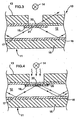
Figure 1 is a schematic cross-sectional view of a tuneable phase shifter or tuneable attenuator in waveguide technology in accordance with the present invention; -
Figure 2 is a schematic cross-sectional view of a tuneable phase shifter or tuneable attenuator in waveguide technology in accordance with the present invention taken along the line A-A inFigure 1 ; -
Figure 3 is a schematic cross-sectional view of radiation propagating through a tuneable phase shifter or tuneable attenuator in waveguide technology in accordance with the present invention; and -
Figure 4 is a further schematic cross-sectional view of radiation propagating through a tuneable phase shifter or tuneable attenuator in waveguide technology in accordance with the present invention. -
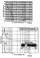
Figure 5 illustrates the Absorbtion coefficient a of Si (in mm-1) versus photon wavelength (in nanometers). -
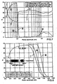
Figure 6 illustrates the refraction index of Si versus photon wavelength in nanometers,Figure 7 the percentage of light reflected transmitted and absorbed by Si versus photon wavelength in nanometers (curves I, II and III respectively), andFigure 8 the percentage of light absorbed by Si versus photon wavelength (in nanometers) for three differentSi wafer thicknesses 50 µ (I), 100 µ (II) and 600 µ (III). -
Figures 9 and 10 show the dielectric constant and tan δ of Si respectively at 40 GHz and 250 Hz. -
Figure 11 shows the wavelength (in millimetres) inside a WR-28 waveguide versus frequency in the Ka band and versus a change in the parameter a (the longest dimension of the waveguide). -
Figures 12a and 12b show an inhomogeneously filled waveguide with a dielectric piece of thickness t in a wall thereof and the fundamental mode TE10 therein. -
Figure 13 shows curves of the wavelength (in millimeters) as a function of frequency (GHz) inside a WR-28 waveguide with a 300 µ thick piece of Si in a wall thereof under different light conditions. -
Figure 14 shows curves of the wavelengths (in millimeters) as a function of frequency (GHz) for a WR-28 waveguide with a piece of Si in a wall thereof withdifferent thicknesses 300 µ (I), 500 µ (II), 1000 µ (III and IV), and two different light conditions for the thickness of 1000 µ. - The
tuneable phase shifter 10 illustrated inFigures 1 and 2 comprises awaveguide 11 having acentral channel 12 which extends the length of thewaveguide 11 and an aperture formed in aside 13 of thewaveguide 11. Thetuneable phase shifter 10 may further comprise ametallic grid 20 to avoid radiation of the microwave, mm-wave or submm-wave inside the waveguide to be lost outside the waveguide system. - A photo-
responsive layer 18 is disposed within thechannel 12 of thewaveguide 11 so as to extend substantially across the aperture. An adjustable irradiation source oflight 14 emits light at a certain part of the spectra where the photo responsive material inside the waveguide absorbs it better (infrared, visible, ultraviolet...). Source oflight 14 is located outside the waveguide such that irradiating radiation from thesource 14 is incident upon an area of the photo-responsive layer 18 exposed by theaperture 30 formed in aside 13 of thewaveguide 11. The photoconductive material is placed directly against the waveguide wall and is illuminated through the wall against it is placed. If the intensity of light is sufficient, a quasi-metallic layer is formed at the waveguide wall/photo-responsive material boundary which is closest to the waveguide wall. This layer changes the effective width of the waveguide which results in a change in effective guide wavelength and hence phase. As the thickness of the quasi-metalliclayer 26 is depended on the light intensity, so is the phase shift. - The photo-
responsive layer 18 may be of semiconductive material, e.g. Si, AsGa, Ge. - The
waveguide 11 comprises a silicon ormetallic body 15 having acentral channel 12 substantially rectangular in cross-section extending the length of thesilicon body 15. The width and height of thechannel 12 may be as is conventionally employed in rectangular waveguide construction. However, the dimensions of thesilicon body 15 may be adjusted according to preference. - The
inner surfaces 16 of thesilicon body 15 may be coated with ametallic film 17, preferably using for example vacuum deposition and electroplating techniques. Suitable metals for coating thesilicon body 15 include, but are not limited to, nickel, copper, brass, chromium, silver and gold. Themetal coating 17 acts to reflect radiation propagating along the length of thechannel 12. Accordingly, thecoating 17 may comprise any material which serves to reflect radiation. - Alternatively, a completely metallic waveguide made for example by a milling machine may be used.
- A construction of metallised silicon waveguides for terahertz applications using micromachining techniques is known and is described for example in "Silicon Micromachined Waveguides for Millimeter and Submillimeter Wavelengths", Yap et al., Symposium Proceedings: Third International Symposium on Space Terahertz Technology, Ann Arbor, MI, pp. 316-323, March 1992 and "Micromachining for Terahertz Applications", Lubecke et al., IEEE Trans. Microwave Theory Tech., Vol. 46, pp. 1821-1831, Nov. 1998.
- The aperture formed in the
side 13 of thewaveguide 11 extends through thesilicon body 15 and themetal coating 17 on one of the longer sides of thewaveguide 11. The aperture may be rectangular in shape and with a width substantially similar to the width of thechannel 12. The length of the aperture is characterised by the desired degree of phase shifting at the frequency of operation. Generally speaking, the longer the length of the aperture (or rather the longer the exposed region of the photo-responsive reflector 18), the greater the degree of phase shifting and/or attenuation. - The
semi-conductor layer 18 may be associated with a plurality ofreflective elements 20. The layer of photo-responsive semi-conductor layer 18 has for example an upper 21 and lower 22 surface substantially rectangular in shape. The width of thelayer 18 may be substantially similar to the width of thechannel 12, whilst the length of thelayer 18 is preferably longer than the length of the aperture formed on theside 13 of thewaveguide 11. Preferably the length of thelayer 18 is only slightly longer than that of the aperture. Thelayer 18 is secured within thechannel 12 of thewaveguide 11 such that thelayer 18 extends substantially across the aperture formed in theside 13 of thewaveguide 11. The layer of photo-responsive material 18 is secured to awall 23 of thechannel 12 for example by a thin layer of adhesive applied at theends layer 18 extending beyond the length of the aperture. Alternatively, if the waveguide is made of metallised silicon,layer 18 may be integral with the waveguide. - The photo-
responsive material 18 may be photo-conductive preferably consists substantially of intrinsic silicon. However, alternative photo-responsive materials which may be used include, but are not limited to, GaAs and Ge. - When the optical radiation is incident upon the exposed
surface 21 of the photo-responsive layer 18, photo-excited carriers are created at a region near thesurface 21. Accordingly, the dielectric constant of the photo-responsive material 18 in this region changes ; generally referred to as photo-induced reflectivity. The reflectivity of theirradiated surface 21 of the photo-responsive material 18 can even be rendered similar to that of a metal in dependence upon the intensity of the incident optical radiation, but with this device it is sufficient to have a small increase of the real part of the dielectric constant associated with a large increase of the imaginary part of the dielectric constant. At this point, the photo-responsive material 18 can be regarded as having a separate photo-induced resistive layer (reference numeral 26 inFigure 4 ), but for a thin layer, the effect of the light is to change the dielectric properties of the material in depth, i.e. essentially the imaginary part of the dielectric constant in all the thickness. - Whilst the photo-
responsive material 18 is generally transparent to the radiation propagating along thechannel 12 of thewaveguide 11, some power loss of the signal will occur. Accordingly, the thickness of the layer of photo-responsive material 18 may be for example between 60 and 100 µm. A higher thickness up to about 1000 µm may be used. Moreover, the photo-responsive material 18 is preferably silicon. - The lifetime of the photo-excited carriers are determined primarily by their mobility and the availability of recombination sites in the lattice of the photo-
responsive material 18. By increasing the lifetime of the carriers, the lifetime of the photo-induced reflective layer can be extended. Accordingly, the irradiation delivered by thesource 14 may be delivered over shorter periods of time. Not only does this reduce the amount of power consumed by the irradiation source but it also prevents the photo-responsive material 18 from reaching potentially damaging temperatures which can arise from continuous irradiation. In order to increase the lifetime of the carriers, the photo-responsive layer 18 preferably has a high electrical resistivity (> 1 kΩcm-2). The photo-responsive layer 18 may consist of silicon having an electrical resistivity for example between 4 and 10 kΩcm-2. - Moreover, the lifetime of the carriers can be further increased for example by pacifying the
irradiated surface 21 of the photo-responsive material 18. Thesurface 21 of the photo-responsive layer 18 offers a large number of recombination sites. By pacifying theirradiated surface 21, the number of recombination sites available to the carriers is significantly reduced. Theuppermost surface 21 of the photo-responsive material is therefore preferably oxidised. Even with oxidation, however, the number of recombination sites remains sufficiently high to significantly affect the mobility of carriers. It has been found, however, that applying a coating of an adhesive such as an epoxy resin to the oxidised surface of the photo-responsive material can significantly increase carrier lifetime. - In having a photo-
responsive layer 18 comprising essentially of high resistance silicon for example with a resistivity of between 4 and 10 kΩcm-2 and an oxidised upper surface coated in an epoxy resin, the lifetime of the photo-induced carriers and thus the photo-induced reflective layer is substantially increased. - Accordingly, phase shifting may be achieved and maintained with relatively low intensity irradiation. However, in extending the lifetime of the photo-induced carriers, the response time of the phase shifter is increased.
- It will, however, be appreciated that fast response times can be achieved by having a photo-responsive material in which the lifetime of the photo-induced carriers is relatively short. This may be achieved, for example, by having a photo-responsive layer of low resistance and whose surfaces have not been pacified.
- The plurality of
reflective elements 20 are formed on theuppermost surface 21 of the photo-responsive material 18 in the region defined by the aperture on theside 13 of thewaveguide 11. Thereflective elements 20 are preferably strips of reflecting material. Accordingly, thereflective elements 20 are strips of metal, that may be arranged as a grid. they allow that most part of light entering the photoresponsive material. Again, suitable metals include, but are not limited to, nickel, copper, brass, chromium, silver and gold. The strips are preferably aligned on thesurface 21 of the photo-responsive material 18 so as to extend substantially parallel to the width of thechannel 12 and thus perpendicular to the length of thechannel 12. The length of the strips may be at least the width of thechannel 12 and preferably extend across the full width of the photo-responsive material 18. The strips are evenly spaced (or tapered) along the length of the photo-responsive material 18 and cover preferably less than 50% of the region of thesurface 21 revealed by theaperture 30. The width and separation of the strips is preferably no greater than 1 mm (this of course depends on frequency of operation). The strips should be of a thickness suitable for total reflection of incident radiation without any substantial loss. The strips may be applied, for example, by applying a mask to thesurface 21 of the photo-responsive material 18 and depositing a metal film using vapour deposition. - The
irradiation source 14 may be any source capable of generating photo-induced carriers reflectivity in thelayer 18 of photo-responsive material and is preferably a commercially-available laser or LED array having a visible or near-infrared wavelength, (in fact having the best frequency spectra for absortion by the photo responsive material used). The power required of thesource 14 will depend upon, among other things, the type of photo-responsive material 18 and the degree of phase shifting or attenuation required. - An electronic circuit can control the degree of phase shifting or attenuation by means of the illumination of the photoresponsive material.
- Referring now to
Figure 3 , radiation propagating along the length of thechannel 12 of thewaveguide 11 is reflected internally by the surfaces of themetal coating 17. When the radiation is incident upon the photo-responsive material18, the radiation propagates a little inside it due to its reduced dielectric constant. Upon reaching theuppermost surface 21 of the layer of photo-responsive material 18, a proportion of the radiation is reflected back towards thechannel 12 by the plurality ofreflective elements 20. A small fraction of the radiation is transmitted into the air (indicated by a broken line) and thus exits thewaveguide 11. Owing to the angle of incidence of the propagating radiation with respect to the photo-responsive material 18, no internal reflection occurs within the photo-responsive material 18. Accordingly, the radiation reflected by thereflective elements 20 propagates back through the photo-responsive material 18 and into thechannel 12. The propagating radiation may be incident upon the photo-responsive material 18 more than once, according to the length of thereflector 18, before it continues propagating along with length of thechannel 12 of thewaveguide 11. -
Figure 4 illustrates the situation whereupon irradiating radiation delivered by theirradiation source 14 is incident upon the photo-responsive reflector 18. The irradiating radiation generates carriers in the photo-sensitive material and causes a photo-induced resistivity in photo-responsive material 18. The effective thickness or depth of the photo-inducedresistive layer 26 will depend upon the wavelength and intensity of the irradiating radiation incident upon the photo-responsive material 18. When the radiation propagating along thechannel 12 of thewaveguide 11 is incident upon the photo-responsive layer 18, the radiation propagates through the photo-responsive material 18 only so far as the photo-inducedreflective layer 26. Upon reaching the photo-inducedresistive layer 26, the propagating radiation is reflected back towards thechannel 12. - The photo-induced lossy material in
layer 18 changes the modal propagation in the waveguide so that no field will enter the lossy photoilluminated material but the change in the fundamental mode of that new waveguide will effectively change the phase. The propagating radiation now has a phase (or amplitude) that is substantially different to radiation propagating along thewaveguide 11 in the absence of the photo-sensitive layer 18. Furthermore, phase shifting will occur every time the propagating radiation is incident upon the photo-responsive layer 18. Accordingly, the length of the photo-responsive layer 18 that is illuminated will also determine the degree of phase shifting. This illumination length may be adjustable to adjust phase shift and/or attenuation. As the changes in the modal propagation in the waveguide are determined by the intensity and wavelength characteristics of the irradiating radiation, the degree of phase shifting can accordingly be controlled by varying the intensity and/or wavelength of the irradiating radiation delivered by thesource 14. - In the device shown in
figures 1 to 4 , the silicon is illuminated on its face adjacent to the waveguide wall. This is essential to the invention, as the electric field in a rectangular waveguide is highest in the middle of the guide and zero at the edge, therefore a lossy material that would be placed further towards the centre of the waveguide would absorb more energy than if it were placed at the edge. For a phase shifter the most desirable features is low insertion loss and large phase shift for small power requirement. When the phase shifter is illuminated at low light levels photo carriers are generated changing the resistivity of the material, however, also the imaginary part of the dielectric constant is varied. As the light intensity is increased eventually the silicon takes on metallic properties. In order to achieve a "quasi metallic layer" within the silicon there must be a high density of carriers 1018-1021 carriers/cm3 .It is important to note, however, that this quasi metallic state is not an abrupt change from high resistivity to low resistivity but one that varies exponentially between the each extreme. On one side of the region (the one that is illuminated) there is a nearly metal state, the other has a high resistivity state and in between a lossy resistive state. It is this region within the silicon that causes the majority of the insertion loss. This lossy layer will always be on the opposite side of the quasi metal state region than the side thereof that is being illuminated as the light is decaying exponentially throughout the thickness of the silicon. When as in the present invention, the silicon layer adjacent the waveguide wall is illuminated from the outside, it starts to form first at the outside of the waveguide, hence the insertion loss is kept to a minimum. At lower light intensity, the lossy resistive region will be also at the outside of thematerial 18. In the prior art patents (US 4,263,570 andUS 5,099,214 ) where illumination is from the opposite waveguide wall, the lossy layer forms first inside the waveguide at a distance from the waveguide wall that is equal to the thickness ofsilicon material 18. This is a fundamental difference and will mean that the insertion loss will always be higher. In addition, this position is fixed physically with respect to the waveguide wall. This means that the any resistivity variation within the silicon will occur between the innermost edge of the silicon and the waveguide wall. Consequently it will have a relatively small effect with respect to changing the effective width of the waveguide. With an illumination from the outside as in the present device, the opposite is true. - The dimensions of the
channel 12 of thewaveguide 11, the size and characteristics of the photo-responsive reflector 18 and the size of the aperture formed on theside 13 of thewaveguide 11 may all be tailored to suit the desired performance of thephase shifter 10. An example of the dimensions that might be used for phase shifting terahertz frequencies is now described. The width and height of thechannel 12 is preferably around 1.5 mm and 0.75 mm respectively. This provides a waveguide cut-off frequency of around 0.1 THz. Accordingly, the silicon wafer used to construct thesilicon body 15 has a thickness of around 0.75 mm. Themetal coating 17 is preferably of the order of 500 nm. The width of theaperture 30 formed on theside 13 of the waveguide is also preferably 0.75 mm. The length of theaperture 30 is preferably around 2 cm. The layer of photo-responsive material 18 preferably has a width, length and thickness of around 0.75 mm, 2.5 cm and 70 µm respectively and has an oxidation layer on theuppermost surface 21 typically or around 10-50 nm. Each reflecting element preferably has a width, length and thickness of around 0.5 mm, 0.75 mm and 500 nm respectively. The spacing between reflecting elements is preferably 0.5 mm. - Whilst the embodiment described above comprises a waveguide having a single aperture and a single photo-
responsive layer 18 extending across the aperture, it will be appreciated that two apertures may be formed on opposing sides of thewaveguide 11. Two or more photo-responsive layers would then be employed and the degree of phase shifting or attenuation achievable may be doubled, tripled or quadrupled. It will be appreciated that the same technical effect might be achieved by doubling the length of the single aperture and photo-responsive reflector 18. Nevertheless, a phase shifter comprising two ormore apertures 30 and two or more photo-responsive layers 18 might be considered when the size, and in particular the length, of the phase shifter is a serious consideration. - It will be appreciated that the plurality of reflecting
elements 20 may be omitted. In this situation, some form of irradiating radiation must be delivered to the photo-responsive reflector 18 such that a photo-inducedreflective layer 26 is continuously present. For example, theirradiation source 14 may continuously irradiate the photo-responsive reflector 18 with radiation. Alternatively, theirradiation source 14 may deliver pulsed, high intensity irradiation. - Rather than forming a plurality of
reflective elements 20 on thesurface 21 of the photo-responsive material 18 facing the aperture, thereflective elements 20 could be formed on a separate element such as a glass plate. The glass plate could then be placed within the aperture so as to rest on top of the photo-responsive material 18. - The
phase shifter 10 may also comprise an attenuator, such as a variable attenuator, to compensate for variations in the amplitude of the propagating radiation with phase shift, or a simple tuneable attenuator, not necessarily adjoining to the phase shifting device. Moreover, both phase and amplitude modulation of a signal is then possible. - Signals at millimetre wavelengths require a waveguide having larger dimensions than that for terahertz (sub-millimetre) frequencies. Accordingly, the degree of possible phase shifting is reduced owing to the reduced ratio of the photo-induced layer thickness with respect to the waveguide height. However, this reduction in phase shifting can be compensated by having a photo-
responsive reflector 18 greater in length. - As the photo-
responsive material 18 is generally transparent to the propagating signal, signal distortion and power loss is generally low in comparison to ferroelectric phase shifters. - The following relates to the advantage obtained for a phase shifter from the optical properties of silicon which, as been identified by the inventors, allows a change in the complex relative permitivity of the silicon as it is illuminated by a source of light in infrared wavelengths.
- Illumination of silicon by means of a near-infrared/visible light source produces the generation of electron-hole pairs, thus producing a plasma. This plasma is directly dependant on the intensity and wavelength of the incident light.
- If we assume normal incidence of the light to the silicon wafer, the formulas that explain the properties of the material are as follows:
- The amount of light reflected in an interface air-silicon is:
- For absorption coefficient values greater than zero, the percentage R of total light reflected can be determined using the following equation :

figure 5 . And t is the thickness of the silicon wafer. - Each term in the infinite series is associated with the successive reflections as the light bounces between the surfaces of the silicon wafer. Similarly, the percent transmission T can be determined using the following equation:


- There are essentially two regions of strong optical absorption in Silicon.
Figure 5 shows the absorption coefficient versus photon wavelength for the visible-FIR and IR regions respectively. For photon energies equal-to- or-greater-than the energy gap, normal optical absorption with the generation of free carriers occurs. - In
figure 6 , a plot of the refraction index of silicon material is depicted against wavelength (in nanometers). The refraction index has its maximum at the violet color of the spectrum, this means that violet-blue light is reflected by silicon stronger than other visible colors so we see this material as violet-blue coloured. - In
figure 7 we can see the amount of light power absorbed, reflected and transmitted by a silicon wafer of 600 µm thickness. The maximum absortion occurs for red color visible light and near infrared wavelengths. - Also in
figure 8 , a comparison of three different thicknesses wafers is depicted in terms of light power absorbed by the material, to illustrate the percentage of light absorbed by silicon versus photon wavelength (in nanometers). - The semiconductor complex relative permittivity containing electron-hole pairs is expressed as a sum of two, electron (e) and holes (h) dependant terms:


- For computation reasons: ε0 = 8.854·10-12 F · m -1, ve =4.53.1012 s -1, vh =7.71·1012 s -1, me =0.259·m 0, mh = 0.38·m 0, m 0 = 9.107·10-28 · 10-28 g is the free electronic mass and N is the number of carriers generated in the plasma.
- The dielectric constant of a material is defined as a real and an imaginary part. The relation between the real and the imaginary part is what we call the tan(δ) of a material. This important material parameter is directly related with the losses of that material when an electromagnetic wave passes through it.
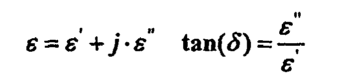
- In the following figures, a plot of the dielectric constant and the tan(δ) of silicon at different frequencies respectively 40 GHz and 250 GHz is depicted against the carrier concentration, N between 1010 and 1020/cm3.
- For example, it can be seen in
figure 9 that at a carrier concentration of 1017 cm-3, the real part of the dielectric constant of the silicon at 40 GHz is 85.6 and at N=1018 cm-3 is 750 where the silicon has a really high dielectric constant. At N above 1017 cm-3, the real and imaginary part of the dielectric constant of the silicon increase with the same slope, so the tan(δ) becomes constant. - At no light condition, the amount of carriers in the silicon is around 1010 cm-3 where the tan(δ) is around 10-4 at 40 GHz. But as the carrier concentration increases with light, the silicon becomes a very lossy material maintaining its dielectric constant quite stable. As it will be seen in the following passages of the description, it is interesting for phase shift to change the dielectric constant of silicon material to affect the propagation characteristics of electromagnetic waves, rather than changing the losses of the material which will attenuate the wave and which is interesting for the attenuator function of the device. So a certain amount of light per area is required.
- In
figure 10 it can be seen that at higher mm-wave frequencies, (250 GHz), the real part of the dielectric constant of the material behaves exactly as at 40 GHz, but the imaginary part is lower, but increases with light with the same slope, so in fact, the losses are lower at higher mm-wave frequencies. - From the understanding of the previous properties, it can be said that changes in the dielectric material properties of silicon by means of an optical source of variable intensity can be achieved. This property opens a new field of applications to design and manufacture a wide variety of components at mm-wave frequencies by means of photoillumination. We assume in our finite element calculations by means of Ansoft-HFSS that the plasma thickness remains constant while the plasma density varies in this thickness with intensity of applied light.
- The main reason of this study is to design, manufacture and measure a phase shifter for rectangular waveguide technology. The tuneable phase shifter has to achieve a phase shift with high accuracy and as low losses as possible. A best mode is a tuneable shifter with a 360° phase shift. A piece of silicon is placed inside the rectangular waveguide and its dielectric properties changed by means of appropriate conditions of photoillumination. If a certain size piece of silicon is placed inside a rectangular waveguide and is illuminated, it changes the propagation characteristics of the waveguide and the transmision characteristics of the waveguide.
- The illumination may be performed by means of a metallic grid in one of the walls of the waveguide so that it is transparent for light and "metallic" for mm-waves so that the characteristics of the rectangular guide do not change.
- Also, a certain amount of light required to perform a change in the propagation properties of the waveguide with a silicon piece inside. In fact, it easy to check that as the wavelength increases, the amount of light per unit area will be lower, because the silicon piece needed to perform the change will be smaller. In fact, if we increase the frequency by a factor of 10, the amount of light per unit area required will decrease by a factor of 100.
- For ease of manufacture and measurement reasons the design given as example was prepared in Ka band for WR-28 standard waveguide. The dimensions of this waveguide are a = 7.1 mm and b = 3.6 mm, and in
figure 11 it can be seen the wavelength inside this waveguide against frequency. Also infigure 11 , we can see the effects on the wavelength (in mm) inside a WR-28 waveguide of a change of its parameter a from 7.1 mm to 5 mm - The wavelength inside a rectangular waveguide is defined by:

- This formula means that if we change the (a) parameter in a rectangular waveguide we will change its wavelength and in fact the phase for a certain length of waveguide. So if we place a piece of silicon in one of the waveguide walls and we change its dielectric constant from 11.8 to above 100 in fact we will change the (a) dimension of the waveguide changing its inside wavelength for a certain frequency.
- The amount of phase change will depend then of the thickness on the silicon piece, its position inside the waveguide, its length and the dielectric constant of the photoilluminated silicon that we will achieve. Special care must be taken to avoid losses in the waveguide if we try to achieve a big phase change in a short length and we push the waveguide near cut off because the return losses of the device will increase a lot.
- If we analyse a rectangular waveguide with a piece of silicon in one of the walls, (see
figure 12a ), we can conclude that happens a mode propagation that is very smilar to the normal rectangular waveguide. In fact, as can be seen infigure 8b , the fundamental mode is very similar to the TE10 of normal rectangular waveguide [Field Theory of Guided Waves, Collin], this mode has the advantage that only a small amount of the field will travel inside the silicon insert, so the losses will be low, and the cutoff frequency of this type of waveguide is lower than in a normal rectangular waveguide, (also an advantage, besides we must be careful with other modes that can appear at the higher frequencies of the band). - In
figure 13 it can be seen the wavelength of a WR-28 waveguide with a 300 µm thick piece of silicon in the wall of the waveguide under dark and illuminated conditions. - As shown in
figure 13 , the wavelength of a normal WR-28 waveguide and the same waveguide filled with a 300 µm thick silicon in the wall under dark condition is nearly the same. Upon illumination of the silicon, the dielectric constant changes inside it and produces a change in the wavelength and in fact in the phase. To achieve an efficient phase change in a short device, the change of the dielectric constant of the silicon by means of photoillumination must be high. - As an example, if we change the dielectric constant of the material from 11.9 to 500, we need a length of 40 mm of silicon to achieve a total 360 degrees phase change in the whole Ka band, but if we only reach a dielectric constant of 100 a length of nearly 300 mm of silicon is needed. So the device will be in the latter case not very practical if the aim is to obtain a 360° phase shift.
- To reach a dielectric constant of 500 to allow an efficient and compact device over an area of 40x3.6 mm, means, see
figure 5 that, the carrier concentration must be above 1018 which is quite high. Such a high density plasma will not be reached with a normal light equipment and a costly equipment will be needed. - It can be seen from
figure 14 , that if a thicker silicon piece of 1 mm thickness is used, a length of 15 mm silicon that changes its dielectric constant from 11.9 to 50 will suffer to achieve a 360° phase change in the whole Ka band. This means a carrier concentration around 5·1016 which is easily obtainable.

Claims (7)
- A tunable phase shifter and/or attenuator comprising a waveguide (11) having a channel (12) defined by internal walls of the waveguide (11) and a piece of photo-responsive material (18) disposed within the waveguide (11) and said piece of photo-responsive material having an outside surface (21) directly in contact with an internal wall (23) of said channel (12), a light source (14) located outside the waveguide (11) to emit light through an aperture (30) of said internal wall (23), characterized in that said light source (14) is disposed to impinge light on at least part of the outside surface (21) of said piece of photo-responsive material (18).
- The tuneable phase shifter and/or attenuator as in claim 1, wherein the photo-responsive material (18) is a photo-conductive material, e.g. Si, GaAs or Ge.
- The tuneable phase shifter and/or attenuator as in claim 1 or 2 wherein at least the outside surface (21) of the piece of photo-responsive material (18) facing the aperture is pacified by oxidation.
- The tuneable phase shifter and/or attenuator as in claim 3, wherein at least the outside surface (21) of the piece of photo-responsive material (18) facing the aperture has a coating of an epoxy resin.
- The tuneable phase shifter and/or attenuator as in any one of the preceding claims, wherein at least part of the outside surface (21) the piece of photo-responsive material (18) facing the aperture is covered with strips (20) of reflective elements to avoid radiation inside the waveguide (11) to be lost outside.
- The tuneable phase shifter and/or attenuator as in claim 5, wherein said strips (20) form a grid.
- The tuneable phase shifter and/or attenuator as in any one of the preceding claims, wherein the light source (14) is adjustable to generate in said piece of photo-responsive material (18) a carrier concentration between 1018 cm-3 and 1021 cm-3.
Priority Applications (1)
| Application Number | Priority Date | Filing Date | Title |
|---|---|---|---|
| EP08075129A EP1923949A1 (en) | 2002-10-25 | 2003-10-24 | Tuneable phase shifter and/or attenuator |
Applications Claiming Priority (3)
| Application Number | Priority Date | Filing Date | Title |
|---|---|---|---|
| GB0224911 | 2002-10-25 | ||
| GBGB0224911.8A GB0224911D0 (en) | 2002-10-25 | 2002-10-25 | Tuneable phase shifter |
| PCT/EP2003/013336 WO2004038849A1 (en) | 2002-10-25 | 2003-10-24 | Tuneable phase shifter and/or attenuator |
Related Child Applications (1)
| Application Number | Title | Priority Date | Filing Date |
|---|---|---|---|
| EP08075129A Division EP1923949A1 (en) | 2002-10-25 | 2003-10-24 | Tuneable phase shifter and/or attenuator |
Publications (2)
| Publication Number | Publication Date |
|---|---|
| EP1559166A1 EP1559166A1 (en) | 2005-08-03 |
| EP1559166B1 true EP1559166B1 (en) | 2009-02-18 |
Family
ID=9946611
Family Applications (2)
| Application Number | Title | Priority Date | Filing Date |
|---|---|---|---|
| EP03809338A Expired - Lifetime EP1559166B1 (en) | 2002-10-25 | 2003-10-24 | Tuneable phase shifter and/or attenuator |
| EP08075129A Withdrawn EP1923949A1 (en) | 2002-10-25 | 2003-10-24 | Tuneable phase shifter and/or attenuator |
Family Applications After (1)
| Application Number | Title | Priority Date | Filing Date |
|---|---|---|---|
| EP08075129A Withdrawn EP1923949A1 (en) | 2002-10-25 | 2003-10-24 | Tuneable phase shifter and/or attenuator |
Country Status (13)
| Country | Link |
|---|---|
| US (1) | US7283019B2 (en) |
| EP (2) | EP1559166B1 (en) |
| JP (2) | JP4502813B2 (en) |
| KR (1) | KR20050083822A (en) |
| CN (1) | CN100553029C (en) |
| AT (1) | ATE423400T1 (en) |
| AU (1) | AU2003301592A1 (en) |
| CA (1) | CA2503545A1 (en) |
| DE (1) | DE60326261D1 (en) |
| DK (1) | DK1559166T3 (en) |
| ES (1) | ES2322582T3 (en) |
| GB (1) | GB0224911D0 (en) |
| WO (1) | WO2004038849A1 (en) |
Families Citing this family (15)
| Publication number | Priority date | Publication date | Assignee | Title |
|---|---|---|---|---|
| JP4950769B2 (en) * | 2007-05-30 | 2012-06-13 | 浜松ホトニクス株式会社 | Terahertz wave neutralization filter |
| US8952678B2 (en) | 2011-03-22 | 2015-02-10 | Kirk S. Giboney | Gap-mode waveguide |
| TWI595219B (en) * | 2012-05-08 | 2017-08-11 | 新力股份有限公司 | Infrared conversion element, imaging device and imaging method |
| US20130315527A1 (en) * | 2012-05-25 | 2013-11-28 | Xiaochen Sun | Photocarrier-injecting variable optical attenuator |
| CN104157933A (en) * | 2014-09-01 | 2014-11-19 | 无锡华测电子系统有限公司 | Microminiature adjustable microwave broadband phase shift attenuator |
| US9634650B2 (en) * | 2015-06-26 | 2017-04-25 | Peregrine Semiconductor Corporation | State change stabilization in a phase shifter/attenuator circuit |
| US9817250B2 (en) | 2015-07-21 | 2017-11-14 | Samsung Electronics Co., Ltd. | Optical modulator including nanostructure |
| CN105070978A (en) * | 2015-08-18 | 2015-11-18 | 中国科学技术大学 | Non-contact type light-operated high-power waveguide phase shifter |
| WO2018170555A1 (en) * | 2017-03-24 | 2018-09-27 | Macquarie University | Improvements in terahertz lasers and terahertz extraction |
| CN109597149B (en) * | 2017-09-30 | 2020-03-27 | 中国石油大学(北京) | Novel terahertz attenuator used in terahertz functional device |
| EP3879623B1 (en) * | 2020-03-11 | 2025-08-27 | Nokia Technologies Oy | Apparatus comprising a waveguide for radio frequency signals |
| CN115000680B (en) * | 2021-03-02 | 2023-10-31 | 上海中航光电子有限公司 | An antenna, phase shifter and communication equipment |
| CN115000681B (en) * | 2021-03-02 | 2024-04-26 | 上海天马微电子有限公司 | Antenna and preparation method thereof, phase shifter, and communication device |
| CN115036658B (en) * | 2021-03-05 | 2025-01-17 | 上海天马微电子有限公司 | Phase shift unit and manufacturing method thereof, phase shifter, and antenna |
| CA3219797A1 (en) * | 2021-05-10 | 2022-11-17 | Purdue Research Foundation | Semiconductor system with waveguide assembly with rf signal impedance controllable by applied electromagnetic radiation |
Family Cites Families (9)
| Publication number | Priority date | Publication date | Assignee | Title |
|---|---|---|---|---|
| US2856589A (en) * | 1954-04-20 | 1958-10-14 | Rca Corp | Light-controlled waveguide attenuator |
| US4263570A (en) * | 1978-10-24 | 1981-04-21 | The United States Of America As Represented By The Secretary Of The Navy | Optical phase shifter |
| JPS63232601A (en) * | 1987-03-20 | 1988-09-28 | Fujitsu Ltd | Band-pass filter for microwave/millimeter wave |
| JPH02248511A (en) * | 1989-03-20 | 1990-10-04 | Mitsui Constr Co Ltd | Composite back-filling material |
| JPH0354901A (en) * | 1989-07-24 | 1991-03-08 | Oki Electric Ind Co Ltd | Waveguide attenuator |
| US5099214A (en) | 1989-09-27 | 1992-03-24 | General Electric Company | Optically activated waveguide type phase shifter and attenuator |
| JPH03187603A (en) * | 1989-12-18 | 1991-08-15 | Arimura Giken Kk | Square waveguide |
| JP3455575B2 (en) * | 1994-03-14 | 2003-10-14 | 株式会社東芝 | Optical semiconductor device |
| JP4164934B2 (en) * | 1999-03-29 | 2008-10-15 | 松下電器産業株式会社 | Variable impedance unit |
-
2002
- 2002-10-25 GB GBGB0224911.8A patent/GB0224911D0/en not_active Ceased
-
2003
- 2003-10-24 EP EP03809338A patent/EP1559166B1/en not_active Expired - Lifetime
- 2003-10-24 US US10/532,737 patent/US7283019B2/en not_active Expired - Fee Related
- 2003-10-24 WO PCT/EP2003/013336 patent/WO2004038849A1/en not_active Ceased
- 2003-10-24 AT AT03809338T patent/ATE423400T1/en not_active IP Right Cessation
- 2003-10-24 KR KR1020057007159A patent/KR20050083822A/en not_active Ceased
- 2003-10-24 CA CA002503545A patent/CA2503545A1/en not_active Abandoned
- 2003-10-24 JP JP2004546029A patent/JP4502813B2/en not_active Expired - Fee Related
- 2003-10-24 ES ES03809338T patent/ES2322582T3/en not_active Expired - Lifetime
- 2003-10-24 EP EP08075129A patent/EP1923949A1/en not_active Withdrawn
- 2003-10-24 DE DE60326261T patent/DE60326261D1/en not_active Expired - Lifetime
- 2003-10-24 CN CNB2003801061214A patent/CN100553029C/en not_active Expired - Fee Related
- 2003-10-24 DK DK03809338T patent/DK1559166T3/en active
- 2003-10-24 AU AU2003301592A patent/AU2003301592A1/en not_active Abandoned
-
2010
- 2010-03-03 JP JP2010046421A patent/JP2010152390A/en active Pending
Also Published As
| Publication number | Publication date |
|---|---|
| JP4502813B2 (en) | 2010-07-14 |
| WO2004038849A1 (en) | 2004-05-06 |
| CN1726613A (en) | 2006-01-25 |
| GB0224911D0 (en) | 2002-12-04 |
| ATE423400T1 (en) | 2009-03-15 |
| AU2003301592A1 (en) | 2004-05-13 |
| JP2006504128A (en) | 2006-02-02 |
| DE60326261D1 (en) | 2009-04-02 |
| DK1559166T3 (en) | 2009-06-15 |
| KR20050083822A (en) | 2005-08-26 |
| EP1559166A1 (en) | 2005-08-03 |
| US20050270121A1 (en) | 2005-12-08 |
| EP1923949A1 (en) | 2008-05-21 |
| JP2010152390A (en) | 2010-07-08 |
| CN100553029C (en) | 2009-10-21 |
| ES2322582T3 (en) | 2009-06-23 |
| CA2503545A1 (en) | 2004-05-06 |
| US7283019B2 (en) | 2007-10-16 |
Similar Documents
| Publication | Publication Date | Title |
|---|---|---|
| JP2010152390A (en) | Tunable phase shifter and/or attenuator | |
| US8450687B2 (en) | Integrated terahertz antenna and transmitter and/or receiver, and a method of fabricating them | |
| US4441789A (en) | Resonance absorber | |
| US7835600B1 (en) | Microwave receiver front-end assembly and array | |
| CN101718943B (en) | Terahertz wave generator | |
| US5360973A (en) | Millimeter wave beam deflector | |
| Acharya et al. | Tapered slotline antennas at 802 GHz | |
| Arzhannikov et al. | Diagnostic system for studying generation of subterahertz radiation during beam-plasma interaction in the GOL-3 facility | |
| Aji | High-performance radiation design of a planar bow-tie antenna combined with a dielectric lens and cascaded matching layers at terahertz frequency | |
| Chelnokov et al. | Light controllable defect modes in three-dimensional photonic crystal | |
| Platte | Optoelectronic microwave switching via laser-induced plasma tapers in GaAs microstrip sections | |
| Platte | Periodic-structure photoexcitation of a silicon coplanar waveguide for selective optoelectronic microwave control | |
| TSUTSUMI et al. | Optical control of millimeter waves in the semiconductor waveguide | |
| HK1112531A (en) | Tuneable phase shifter and/or attenuator | |
| KR20240035749A (en) | Semiconductor system with waveguide assembly having RF signal impedance controllable by applied electromagnetic radiation | |
| Lockyer et al. | Transmission through optically generated inductive grid arrays | |
| JP2004505309A (en) | Optical waveguide filter | |
| US7741934B2 (en) | Coupling a signal through a window | |
| Houghton et al. | High-performance GaAs-GaAlAs phase modulators for PSK optical fibre systems | |
| Fickenscher | Laser-controlled coupling structures for MMW and SubMMW applications | |
| Platte | Microwave measurements of effective dielectric constant of semiconductor waveguides via periodic-structure photoexcitation | |
| Chia et al. | Optically controlled frequency selective surface with semiconductor substrate | |
| Abdelmouty | Terahertz System-on-Chip using coplanar stripline transmission line on thin membrane | |
| RU2052872C1 (en) | Modulator | |
| Gammand et al. | Slow wave propagation using interconnections for IC technologies |
Legal Events
| Date | Code | Title | Description |
|---|---|---|---|
| PUAI | Public reference made under article 153(3) epc to a published international application that has entered the european phase |
Free format text: ORIGINAL CODE: 0009012 |
|
| 17P | Request for examination filed |
Effective date: 20050518 |
|
| AK | Designated contracting states |
Kind code of ref document: A1 Designated state(s): AT BE BG CH CY CZ DE DK EE ES FI FR GB GR HU IE IT LI LU MC NL PT RO SE SI SK TR |
|
| AX | Request for extension of the european patent |
Extension state: AL LT LV MK |
|
| DAX | Request for extension of the european patent (deleted) | ||
| REG | Reference to a national code |
Ref country code: HK Ref legal event code: DE Ref document number: 1080613 Country of ref document: HK |
|
| GRAP | Despatch of communication of intention to grant a patent |
Free format text: ORIGINAL CODE: EPIDOSNIGR1 |
|
| GRAS | Grant fee paid |
Free format text: ORIGINAL CODE: EPIDOSNIGR3 |
|
| GRAA | (expected) grant |
Free format text: ORIGINAL CODE: 0009210 |
|
| AK | Designated contracting states |
Kind code of ref document: B1 Designated state(s): AT BE BG CH CY CZ DE DK EE ES FI FR GB GR HU IE IT LI LU MC NL PT RO SE SI SK TR |
|
| REG | Reference to a national code |
Ref country code: GB Ref legal event code: FG4D |
|
| REG | Reference to a national code |
Ref country code: CH Ref legal event code: EP |
|
| REG | Reference to a national code |
Ref country code: IE Ref legal event code: FG4D |
|
| REF | Corresponds to: |
Ref document number: 60326261 Country of ref document: DE Date of ref document: 20090402 Kind code of ref document: P |
|
| REG | Reference to a national code |
Ref country code: SE Ref legal event code: TRGR |
|
| REG | Reference to a national code |
Ref country code: DK Ref legal event code: T3 |
|
| REG | Reference to a national code |
Ref country code: ES Ref legal event code: FG2A Ref document number: 2322582 Country of ref document: ES Kind code of ref document: T3 |
|
| PG25 | Lapsed in a contracting state [announced via postgrant information from national office to epo] |
Ref country code: SI Free format text: LAPSE BECAUSE OF FAILURE TO SUBMIT A TRANSLATION OF THE DESCRIPTION OR TO PAY THE FEE WITHIN THE PRESCRIBED TIME-LIMIT Effective date: 20090218 |
|
| PG25 | Lapsed in a contracting state [announced via postgrant information from national office to epo] |
Ref country code: AT Free format text: LAPSE BECAUSE OF FAILURE TO SUBMIT A TRANSLATION OF THE DESCRIPTION OR TO PAY THE FEE WITHIN THE PRESCRIBED TIME-LIMIT Effective date: 20090218 |
|
| PG25 | Lapsed in a contracting state [announced via postgrant information from national office to epo] |
Ref country code: BE Free format text: LAPSE BECAUSE OF FAILURE TO SUBMIT A TRANSLATION OF THE DESCRIPTION OR TO PAY THE FEE WITHIN THE PRESCRIBED TIME-LIMIT Effective date: 20090218 |
|
| PG25 | Lapsed in a contracting state [announced via postgrant information from national office to epo] |
Ref country code: CZ Free format text: LAPSE BECAUSE OF FAILURE TO SUBMIT A TRANSLATION OF THE DESCRIPTION OR TO PAY THE FEE WITHIN THE PRESCRIBED TIME-LIMIT Effective date: 20090218 Ref country code: EE Free format text: LAPSE BECAUSE OF FAILURE TO SUBMIT A TRANSLATION OF THE DESCRIPTION OR TO PAY THE FEE WITHIN THE PRESCRIBED TIME-LIMIT Effective date: 20090218 Ref country code: PT Free format text: LAPSE BECAUSE OF FAILURE TO SUBMIT A TRANSLATION OF THE DESCRIPTION OR TO PAY THE FEE WITHIN THE PRESCRIBED TIME-LIMIT Effective date: 20090727 |
|
| PGFP | Annual fee paid to national office [announced via postgrant information from national office to epo] |
Ref country code: FR Payment date: 20090730 Year of fee payment: 7 |
|
| PG25 | Lapsed in a contracting state [announced via postgrant information from national office to epo] |
Ref country code: SK Free format text: LAPSE BECAUSE OF FAILURE TO SUBMIT A TRANSLATION OF THE DESCRIPTION OR TO PAY THE FEE WITHIN THE PRESCRIBED TIME-LIMIT Effective date: 20090218 Ref country code: RO Free format text: LAPSE BECAUSE OF FAILURE TO SUBMIT A TRANSLATION OF THE DESCRIPTION OR TO PAY THE FEE WITHIN THE PRESCRIBED TIME-LIMIT Effective date: 20090218 |
|
| PLBE | No opposition filed within time limit |
Free format text: ORIGINAL CODE: 0009261 |
|
| STAA | Information on the status of an ep patent application or granted ep patent |
Free format text: STATUS: NO OPPOSITION FILED WITHIN TIME LIMIT |
|
| 26N | No opposition filed |
Effective date: 20091119 |
|
| PG25 | Lapsed in a contracting state [announced via postgrant information from national office to epo] |
Ref country code: BG Free format text: LAPSE BECAUSE OF FAILURE TO SUBMIT A TRANSLATION OF THE DESCRIPTION OR TO PAY THE FEE WITHIN THE PRESCRIBED TIME-LIMIT Effective date: 20090518 |
|
| PGFP | Annual fee paid to national office [announced via postgrant information from national office to epo] |
Ref country code: DE Payment date: 20091014 Year of fee payment: 7 Ref country code: DK Payment date: 20091028 Year of fee payment: 7 Ref country code: ES Payment date: 20091026 Year of fee payment: 7 Ref country code: FI Payment date: 20091015 Year of fee payment: 7 Ref country code: SE Payment date: 20091020 Year of fee payment: 7 |
|
| PGFP | Annual fee paid to national office [announced via postgrant information from national office to epo] |
Ref country code: NL Payment date: 20091016 Year of fee payment: 7 |
|
| PGFP | Annual fee paid to national office [announced via postgrant information from national office to epo] |
Ref country code: GB Payment date: 20091014 Year of fee payment: 7 Ref country code: IT Payment date: 20091016 Year of fee payment: 7 |
|
| PG25 | Lapsed in a contracting state [announced via postgrant information from national office to epo] |
Ref country code: MC Free format text: LAPSE BECAUSE OF NON-PAYMENT OF DUE FEES Effective date: 20091031 |
|
| REG | Reference to a national code |
Ref country code: CH Ref legal event code: PL |
|
| PG25 | Lapsed in a contracting state [announced via postgrant information from national office to epo] |
Ref country code: CH Free format text: LAPSE BECAUSE OF NON-PAYMENT OF DUE FEES Effective date: 20091031 Ref country code: LI Free format text: LAPSE BECAUSE OF NON-PAYMENT OF DUE FEES Effective date: 20091031 Ref country code: IE Free format text: LAPSE BECAUSE OF NON-PAYMENT OF DUE FEES Effective date: 20091024 Ref country code: GR Free format text: LAPSE BECAUSE OF FAILURE TO SUBMIT A TRANSLATION OF THE DESCRIPTION OR TO PAY THE FEE WITHIN THE PRESCRIBED TIME-LIMIT Effective date: 20090519 |
|
| PG25 | Lapsed in a contracting state [announced via postgrant information from national office to epo] |
Ref country code: LU Free format text: LAPSE BECAUSE OF NON-PAYMENT OF DUE FEES Effective date: 20091024 |
|
| REG | Reference to a national code |
Ref country code: NL Ref legal event code: V1 Effective date: 20110501 |
|
| REG | Reference to a national code |
Ref country code: DK Ref legal event code: EBP |
|
| GBPC | Gb: european patent ceased through non-payment of renewal fee |
Effective date: 20101024 |
|
| PG25 | Lapsed in a contracting state [announced via postgrant information from national office to epo] |
Ref country code: HU Free format text: LAPSE BECAUSE OF FAILURE TO SUBMIT A TRANSLATION OF THE DESCRIPTION OR TO PAY THE FEE WITHIN THE PRESCRIBED TIME-LIMIT Effective date: 20090819 |
|
| PG25 | Lapsed in a contracting state [announced via postgrant information from national office to epo] |
Ref country code: FR Free format text: LAPSE BECAUSE OF NON-PAYMENT OF DUE FEES Effective date: 20101102 |
|
| REG | Reference to a national code |
Ref country code: FR Ref legal event code: ST Effective date: 20110630 |
|
| PG25 | Lapsed in a contracting state [announced via postgrant information from national office to epo] |
Ref country code: TR Free format text: LAPSE BECAUSE OF FAILURE TO SUBMIT A TRANSLATION OF THE DESCRIPTION OR TO PAY THE FEE WITHIN THE PRESCRIBED TIME-LIMIT Effective date: 20090218 Ref country code: NL Free format text: LAPSE BECAUSE OF NON-PAYMENT OF DUE FEES Effective date: 20110501 Ref country code: GB Free format text: LAPSE BECAUSE OF NON-PAYMENT OF DUE FEES Effective date: 20101024 Ref country code: FI Free format text: LAPSE BECAUSE OF NON-PAYMENT OF DUE FEES Effective date: 20101024 |
|
| REG | Reference to a national code |
Ref country code: DE Ref legal event code: R119 Ref document number: 60326261 Country of ref document: DE Effective date: 20110502 |
|
| PG25 | Lapsed in a contracting state [announced via postgrant information from national office to epo] |
Ref country code: SE Free format text: LAPSE BECAUSE OF NON-PAYMENT OF DUE FEES Effective date: 20101025 Ref country code: CY Free format text: LAPSE BECAUSE OF FAILURE TO SUBMIT A TRANSLATION OF THE DESCRIPTION OR TO PAY THE FEE WITHIN THE PRESCRIBED TIME-LIMIT Effective date: 20090218 |
|
| PG25 | Lapsed in a contracting state [announced via postgrant information from national office to epo] |
Ref country code: DK Free format text: LAPSE BECAUSE OF NON-PAYMENT OF DUE FEES Effective date: 20101031 |
|
| REG | Reference to a national code |
Ref country code: ES Ref legal event code: FD2A Effective date: 20111118 |
|
| PG25 | Lapsed in a contracting state [announced via postgrant information from national office to epo] |
Ref country code: IT Free format text: LAPSE BECAUSE OF NON-PAYMENT OF DUE FEES Effective date: 20101024 |
|
| PG25 | Lapsed in a contracting state [announced via postgrant information from national office to epo] |
Ref country code: ES Free format text: LAPSE BECAUSE OF NON-PAYMENT OF DUE FEES Effective date: 20101025 |
|
| REG | Reference to a national code |
Ref country code: HK Ref legal event code: WD Ref document number: 1080613 Country of ref document: HK |
|
| PG25 | Lapsed in a contracting state [announced via postgrant information from national office to epo] |
Ref country code: DE Free format text: LAPSE BECAUSE OF NON-PAYMENT OF DUE FEES Effective date: 20110502 |