TECHNICAL FIELD
The present invention relates to an electronic camera. More specifically, the
present invention relates to an electronic camera which is applied to a mobile
communication terminal and comprises a camera device and a processor.
PRIOR ART
One example of a conventional electronic camera is disclosed in Japanese Patent
Laying-open No. 2001-231003 laid-open on August 24, 2001. According to the prior art,
an image signal of an object photographed in response to an operation of a shutter button
is temporarily stored in a frame memory, and then recorded on a recording medium after
subjected to signal processings such as YUV conversion and JPEG compression. The
image signal stored in the frame memory is also output to a monitor after subjected to
YUV conversion and thinning-out process, and therefore a still image (freeze image) of
the photographed object is displayed on a monitor screen.
However, the JPEG compression is lossy compression and thus may cause some
quality deterioration in a decompressed image. Meanwhile, the freeze image displayed
on the monitor screen is not an image that has been subjected to compression process and
extension process. Because of this, in the prior art it is impossible to identify from the
freeze image the image quality deterioration appeared on the decompressed image, and
the checking of image quality deterioration requires a shift to a reproduction mode. In the
prior art, consequently, a complicated operation is needed to check a photographed image
for image quality deterioration.
SUMMARY OF THE INVENTION
Therefore, it is a primary object of the present invention to provide an electronic
camera which makes it possible to easily and promptly check a photographed image for
image quality deterioration.
According to the present invention, an electronic camera comprises a camera
device and a processor. The camera device comprises a first generation means for
generating a compressed image signal based on a photographed image signal, and a
second generation means for generating a decompressed image signal based on the
compressed image signal generated by the first generation means. The processor
comprises a first activation means for activating the first generation means in response to
a photographing instruction, a second activation means for activating the second
generation means in response to completion of a generation process by the first
generation means, and an output means for outputting to a monitor the decompressed
image signal generated by the second generation means.
In the camera device, the first generation means generates a compressed image
signal based on a photographed image signal, and the second generation means generates
a decompressed image signal based on the compressed image signal. The processor
activates the first generation means in response to a photographing instruction, and
activates the second generation means in response to the completion of the generating
process by the first generation means. The processor also outputs toward the monitor the
decompressed image signal generated by the second generation means.
That is, when a photographing instruction is provided, a compressed image signal
is generated on the basis of a photographed image signal, and when the compressed
image signal is generated, a decompressed image signal is generated on the basis of the
compressed image signal. The decompressed image signal generated in this way is
output to the monitor. This makes it possible to check the decompressed image for image
quality deterioration in an easy and prompt manner.
It is preferable that the processor temporarily stores in the memory the compressed
image signal generated by the first generation means, and records the compressed image
signal on a recording medium in response to a recording instruction. This avoids
unintended recording of an image of insufficient image quality, resulting in an
improvement of operability.
In the first generation means, if a compression means compresses the
photographed image signal in a specific order, the camera device preferably comprises an
image sensor in which a plurality of light-receiving elements for generating electric
charges corresponding to an optical image of an object are formed, and a reading means
for reading the electric charges generated in the plurality of light-receiving elements in an
order correlating with the specific order. As a consequence, it becomes no longer
necessary to store the photographed image signal in the memory prior to compression,
which allows a reduction in memory capacity.
Preferably, the compression means performs compression in units of a first pixel
block and the reading means performs reading in units of a second pixel block correlating
with the first pixel block. More preferably, the camera device further comprises a color
filter arranged on a front surface of the image sensor and having a plurality of colors of
color elements, and a color separation means for subjecting to color separation electric
charge signals each of which has only color information of one of the plurality of colors.
The second pixel block is larger than the first pixel block, and two second pixel blocks
adjacent to each other are partly overlapping. It is noted that, if the image sensor is a
CMOS type, the reading of electric charges as stated above becomes possible.
In the second generation means, if a decompression means subjects the
compressed image signal to a decompression process and a resolution reduction means
reduces a resolution of the image signal decompressed by the decompression means to
generate the above stated decompressed image signal, a memory for temporarily storing
the decompressed image signal of high resolution becomes unnecessary.
The compression means preferably performs compression in a lossy format. In
such a case, some image quality deterioration occurs in the decompressed image.
In addition, the photographed image signal is preferably a still image signal. Since
image quality deterioration in a still image is more prominent than image quality
deterioration in a moving image, it can be said that a more remarkable effect will take
place in case where the above described process is performed on a still image signal.
The above described objects and other objects, features, aspects and advantages of
the present invention will become more apparent from the following detailed description
of the present invention when taken in conjunction with the accompanying drawings.
BRIEF DESCRIPTION OF THE DRAWINGS
Figure 1 is a block diagram showing one embodiment of the present invention;
Figure 2 is a block diagram showing one example of a structure of a mobile
communication terminal applied to the Figure 1 embodiment;
Figure 3 is a block diagram showing one example of a structure of a camera unit
applied to the Figure 2 embodiment;
Figure 4 is an illustrative view showing one example of a structure of a color filter
applied to the Figure 3 embodiment;
Figure 5 (A) is an illustrative view showing one part of an operation of the Figure
3 embodiment;
Figure 5 (B) is an illustrative view showing one part of an operation of the Figure
3 embodiment;
Figure 6 is a flowchart showing one part of an operation of a main CPU applied to
the Figure 2 embodiment;
Figure 7 is a flowchart showing another part of the operation of the main CPU
applied to the Figure 2 embodiment;
Figure 8 is a flowchart showing one part of an operation of a camera CPU applied
to the Figure 3 embodiment; and
Figure 9 is a flowchart showing another part of the operation of the camera CPU
applied to the Figure 3 embodiment.
BEST MODE FOR PRACTICING THE INVENTION
Referring to Figure 1, a mobile communication system of this embodiment
includes a mobile communication terminal 200 and a plurality of BS's (Base Stations)
100, 100, ... for performing wireless communications. The BS 100 is connected with an
MLS (Mobile Local Switch) 400. The MLS 400 is connected to another MLS 400 via an
MGS (Mobile Gateway Switch) 300. Telephone dialogues, that is, audio data
communications between the mobile communication terminals 200 are carried out via the
BS 100, the MLS 400 and the MGS 300.
The MLS 400 is also connected to a backbone network 600 via a PPM (Packet
Processing Module) 500. The backbone network 600 is connected with a server 700. The
server 700 is connected to the Internet 800 as well.
When the mobile communication terminal 200 transmits packet data, the packet
data is provided to the server 700 via the BS 100, the MLS 400, the PPM 500 and the
backbone network 600. If the transferred packet data is a mail addressed to another
mobile communication terminal 200, the server 700 sends the packet data to the mobile
communication terminal 200 of destination via the backbone network 600, the PPM 500,
the MLS 400, and the BS 100. On the other hand, if the transferred packet data is a
request for access to a web site 800, the server 700 accesses the web site 900 via the
Internet 800, and returns packet data obtained from the access destination to the mobile
communication terminal 200 that is a source of the request. In this case as well, the
packet data is transferred to the mobile communication terminal 200 that is the source of
the request, via the backbone network 600, the PPM 500, the MLS 400, and the BS 100.
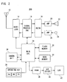
More specifically, the mobile communication terminal 200 is structured as shown
in Figure 2. When a call-out operation for telephone conversation is performed by an
operating key 36, a main CPU 28 transmits a call-out signal to the mobile communication
terminal 200 of the other party through a signal processing circuit 16, a wireless circuit 14
and an antenna 12. When the other party performs a call-in operation in response to this,
a telephone conversation becomes available.
When a voice is input into a microphone 24 after a telephone conversation has
become available, the voice is converted by the microphone 24 into an audio signal as an
analog signal. The converted audio signal is amplified by an amplifier 26 and converted
by an AD/DA conversion circuit 18 into audio data as a digital signal. The converted
audio data is subjected to an encoding process by the signal processing circuit 16, and
also subjected to a modulation process by the wireless circuit 14. The modulated audio
data generated by the wireless circuit 14 is transmitted from the antenna 12.
On the other hand, modulated audio data transmitted from the other party is
received by the antenna 12, subjected to a demodulation process by the wireless circuit
14, and subjected to a decoding process by the signal processing circuit 16. The audio
data decoded by the signal processing circuit 16 is converted by the AD/DA conversion
circuit 18 into an audio signal as an analog signal. The converted audio signal is output
from a speaker 22 via an amplifier 20.
In the middle of a conversation with the other party in this manner, if a
conversation end operation is performed by the operating key 36, the main CPU 28
controls the signal processing circuit 16 and the wireless circuit 14 to transmit a
conversation end signal to the other party. After transmission of the conversation end
signal, the main CPU 28 ends the conversation process. In case where a conversation end
signal is firstly received from the other party as well, the main CPU 28 ends the
conversation process.
When a camera function is enabled by the operating key 36 in a state of no
conversation being held, a through image output process is carried out by the camera unit
34 and the main CPU 28. Firstly, the camera unit 34 photographs an object, generates
low-resolution moving image data corresponding to the photographed object, and outputs
the generated moving image data to the main CPU 28. The main CPU 28 transfers the
moving image data output from the camera unit 34 to a VRAM 38. The moving image
data stored in the VRAM 38 is read out by an LCD driver 40, and thus a real-time moving
image (through image) of the object is displayed on the LCD 42.
When a release key 36a provided in the operating key 36 is operated, an image
compression/save process is carried out by the camera unit 34 and the main CPU 28. In
first, the camera unit 34 generates high-resolution compressed still image data
corresponding to the object at a time when the release key 36a is operated, and outputs the
generated compressed still image data to the main CPU 28. The main CPU 28
temporarily saves in a work memory 34 the compressed still image data supplied from the
camera unit 34.
Upon completion of the image compression/save process, a decompressed image
output process is performed. The camera unit 34 firstly decompresses the compressed
still image data in the JPEG format, reduces a resolution of the decompressed still image
data, and outputs the low-resolution decompressed still image data to the main CPU 28.
The main CPU 28 writes the decompressed still image data output from the camera unit
34 into the VRAM 38. The decompressed still image data stored in the VRAM 38 is read
out by the LCD driver 40, and thus the LCD 42 displays the still image (freeze image) of
the object at a time when the release key 36a is operated.
Since the JPEG format is a lossy format, some image quality deterioration appears
on the decompressed still image data. Accordingly, this image quality deterioration is
also reflected in the freeze image displayed on the LCD 42. An operator can easily and
promptly identify the image quality deterioration from the displayed freeze image.
If a recording key 36b is operated after display of the freeze image on the LCD 42,
the main CPU 28 performs a recording process. More specifically, the compressed still
image data saved in the work memory 34 is recorded by the main CPU 28 on a flash
memory 30. A data file containing the compressed still image is formed in the flash
memory 30 is formed with. Upon completion of recording, the through image output
process is resumed.
Additionally, if a cancel key 36c is operated instead of the recording key 36b, the
through image output process is resumed, bypassing the compressed image data
recording process.
When a mail transmission function is enabled, the main CPU 28 requests the
operator to input a destination address, title and message and select arbitrary compressed
still image data from the flash memory 30. When the destination address, title and
message are input and the arbitrary compressed still image data is selected by operation of
the operating key 36, the main CPU 28 prepares a mail and transmits the mail through the
signal processing circuit 16, the wireless circuit 14 and the antenna 12.
It is noted that a program for realizing the above stated camera function can be
downloaded from a specific web site 900 existing on the Internet 900. The program
downloaded here is written into the flash memory 30.
The camera unit 34 is more specifically structured as shown in Figure 3. An
optical image of the object is irradiated onto a light-receiving surface of a CMOS-type
image sensor 56 through an optical lens 52 and a color filter 54 having a Bayer pattern as
shown in Figure 4. Color elements forming the color filter 54 correspond one by one to
the light-receiving elements (pixels) formed on the light-receiving surface of the image
sensor 56. Generated in each light-receiving element are electric charges having only one
of color information R, G and B.
At a time of the through image output process, a driver 62 drives the image sensor
56 in a raster-scanning mode in response to a vertical synchronizing signal output from a
TG (Timing Generator) 64. The image sensor 56 outputs a raw image signal composed of
the above mentioned electric charges one line by one line. A sensor processing circuit 58
generates raw image data as a digital signal by subjecting a raw image signal of each
frame output from the image sensor 56 to such processes as CDS, AGC, A/D
compression, etc. A camera signal processing circuit 60 generates interpolated image
data by subjecting the generated raw image data to such processes as white-balance
adjustment, color separation, etc. Each of the pixels forming the interpolated image data
is supposed to have all color information of R, G and B. Additionally, the sensor
processing circuit 58 and the camera signal processing circuit 60 perform the processes in
response to a clock signal output from the TG 64.
At the time of the through image output process, a switch SW1 is connected to a
terminal S 1 and a switch S W2 is connected to a terminal S3. The interpolated image data
output from the camera signal processing circuit 60 is provided to a thinning-out circuit
70 via the switch SW1, and subjected to a resolution reduction process. The thinning-out
circuit 70 outputs low-resolution interpolated image data. The interpolated image data is
provided to a memory controller 76 via the switch SW2.
At the time of the through image output process, the memory controller 76
performs so-called bank switching in response to the vertical synchronizing signal output
from the TG 64. More specifically, in writing into a first memory 78a a current frame of
interpolated image data supplied from the switch SW2, the memory controller 76 reads
out a previous frame of interpolated image data from a second frame memory 78b. In
writing into a second frame memory 78b the current frame of interpolated image data
supplied from the switch SW2, the memory controller 76 reads out the previous frame of
the interpolated image data from the first frame memory 78a. Therefore, no overtaking
will occur between a read address and a write address. The consecutive frames of
interpolated image data, that is, the moving image data read by the memory controller 76
are output to the main CPU 28 via an I/F 80.
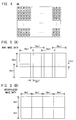
At the time of the image compression/save process, the driver 62 drives the image
sensor 56 for a one-frame period in a block-scanning mode. This causes the image sensor
56 to output one frame of raw image signal in units of pixel blocks each of which is
formed from 10 horizontal pixels x 10 vertical pixels. At this time, an overlap of two
pixels occurs between the pixel blocks adjacent to each other as shown in Figure 5 (A).
This overlap allows for a color separation process in the camera signal processing circuit
60.
The raw image signal output from the image sensor 56 is converted by the sensor
processing circuit 58 into raw image data. The raw image data output from the sensor
processing circuit 58 is converted by the camera signal processing circuit 60 into
interpolated image data. The interpolated image data is output from the camera signal
processing circuit 60 in units of pixel blocks each of which is formed from 8 pixels x 8
pixels as shown in Figure 5 (B).
At the time of the image compression/save process, the switch SW1 is connected
to a terminal S2 and the switch SW2 is connected to a terminal S4. Also, a compression
instruction is provided to an image compression circuit 68, and a bank fixing instruction
is provided to the memory controller 76. By the bank fixing instruction, the first frame
memory 78a is designated as a writing destination and reading destination.
Each pixel block of interpolated image data output from the camera signal
processing circuit 60 is provided to a color conversion circuit 66. A color format of the
interpolated image data is converted from an RGB format to a YUV format. The
converted interpolated image data is supplied in pixel blocks to the image compression
circuit 68 which is activated by the compression request, and is subjected to a
compression process in a lossy format such as JPEG.
The compressed interpolated image data, that is, the compressed still image data is
provided to the memory controller 76 via the switch SW2, and thereby written into the
first frame memory 78a. Since the first frame memory 78a is also designated as a reading
destination, the compressed still image data stored in the first frame memory 78a is read
out later by the memory controller 76. The read compressed still image data is output to
the main CPU 28 via the I/F 80.
At a time of the decompressed image output process, a decompression instruction
is provided to an image decompression circuit 74 and a setting change instruction is
provided to the memory controller 76. By the setting change instruction, the first frame
memory 78a is designated as a reading destination and the second frame memory 78b is
designated as a writing destination. The memory controller 76 reads out the compressed
still image data from the first frame memory 78a, and the image compression circuit 74
activated by the decompression instruction subjects the read compressed still image data
to a JPEG decompression. The decompression process is performed in pixel blocks, and
each pixel block of decompressed interpolated image data, that is, decompressed still
image data is subjected by a color conversion circuit 72 to color conversion from the
YUV format to the RGB format.
The switch SW1 is connected with the terminal S2 at this point in time, and the
decompressed still image data output from the color conversion circuit 72 is supplied to
the thinning-out circuit 70 via the switch SW1. The thinning-out circuit 70 subjects the
supplied compressed still image data to a resolution reduction process, and the resulting
low-resolution decompressed still image data is input to the memory controller 76 via the
switch SW2. The memory controller 76 writes the input decompressed still image data
into the second frame memory 78b.
When the decompression process for one frame has been completed by the image
decompression circuit 74, a setting change instruction is provided to the memory
controller 76. By this instruction, the second frame memory 78b is designated as a
reading destination. The memory controller 76 reads out the decompressed still image
data from the second frame memory 78b, and outputs the read decompressed still image
data to the main CPU 28 via the I/F 80.
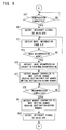
When the camera function is enabled, the main CPU 28 performs a process
according to flowcharts shown in Figure 6 and Figure 7, and a camera CPU 78 performs a
process according to flowcharts shown in Figure 8 and Figure 9. In addition, a control
program corresponding to the flowcharts shown in Figure 6 and Figure 7 is stored in the
flash memory, and a control program corresponding to the flowcharts shown in Figure 8
and Figure 9 is stored in a flash memory 84.
Referring to Figure 6 and Figure 7, a description will be firstly presented as to a
process of the main CPU 28. In a step S1, a prescribed initialization process is carried
out. In a succeeding step S3, a moving image mode is set to the camera unit 34 so as to
perform the through image output process. More specifically, mode information
indicating "moving image mode" is provided to the I/F 80 shown in Figure 3. When the
I/F 80 returns an interrupt signal in response to this mode setting, YES is determined in a
step S5 and one frame of interpolated image data is obtained from the I/F 80 in a step S7.
In a step S9, the obtained interpolated image data is transferred to the VRAM 38. In a
step S11, the presence or absence of an operation of the release key 36a is determined. If
NO, the process returns to the step S3. Thus, unless the release key 36a is pressed, a
plurality of consecutive frames of interpolated image data are fetched from the I/F 80 and
transferred to the VRAM 38.
The plurality of frames of interpolated image data transferred to the VRAM 38 are
sequentially read out by the LCD driver 40. As a result, a moving image composed of the
plurality of frames of interpolated image data, that is, a through image of the object is
displayed on the LCD 42.
When the release key 36a is operated, the process moves from a step S 11 to a step
S 13. In the step S13, an image compression mode is set to the I/F 80 so as to perform the
image compression/save process. When the I/F 80 returns an interrupt signal in response
to this mode setting, YES is determined in a step S15. Then, the compressed still image
data is obtained from the I/F 80 in a step S 17, and the compressed still image data is
transferred to the work memory 32. The obtained compressed still image data is image
data of the object as of a time when the release key 36a is operated. By the process of the
step S 19, the compressed still image data is temporarily saved in the work memory 32.
When storing of the compressed still image data has been completed, an image
decompression mode is set to the I/F 80 in a step S21 so as to perform a decompressed
image output process. When the I/F 80 returns an interrupt signal in response to this
mode setting, YES is determined in a step S23. Then, the decompressed still image data
is obtained from the I/F 80 in a step S25, and the decompressed still image data is
transferred to the VRAM 38 in a step S27. The obtained decompressed still image data is
image data in which the above stated compressed still image data is decompressed and its
resolution is reduced. By the process of the step S27, the decompressed still image data is
written into the VRAM 38. The decompressed still image data stored in the VRAM 38 is
read out by the LCD driver 40. Consequently, the still image, that is, the freeze image of
the object photographed in response to the operation of the release button 36a, is
displayed on the LCD 42.
The presence or absence of an operation of the recording key 36b is determined in
a step S29, and the presence or absence of an operation of the cancel key 36c is
determined in a step S31. When the recording key 36b is operated, the process goes from
the step S29 to a step S33 so as to record the compressed image data saved in the work
memory 32 on the flash memory 30 in a file format. Upon completion of this recording
process, the process returns to the step S3. On the other hand, when the cancel key 36c is
operated, YES is determined in a step S31 and the process returns to the step S3 without
passing the recording process. Accordingly, the through image output process is
resumed.
Next, referring to Figure 8 and Figure 9, a description will be given as to an
operation of the camera CPU 82. A prescribed initialization process is carried out in a
step S41, and the mode information set by the main CPU 28 is obtained from the I/F 80 in
a step S43. It is determined in a step S45 whether or not a content of the mode
information indicates "moving image mode", and it is determined in a step S47 whether
or not the content of the mode information indicates "image compression mode". If YES
is determined in the step S45, the process goes to a step S49 so as to perform the through
image output process. If YES is determined in the step S47, the process goes to a step
S61 so as to perform the image compression/save process. If NO is determined in either
the step S45 or the step S47, the process returns to the step S43.
At the time of the through image output process, the switches SW1 and the SW2
are firstly connected to the terminals S1 and S3 in a step S49. This enables the
thinning-out circuit 70. The driver is instructed to perform raster scanning in a step S51,
and the memory controller 76 is instructed to perform bank switching in a step S53. In a
step S55, it is determined whether or not a vertical synchronizing signal is output from the
TG 64. If YES, an interrupt signal is output to the main CPU 28 via the I/F 80 in a step
S57. When the operation of the step S57 has been completed, the process returns to the
step S43. Therefore, as long as the moving image mode is set to the I/F 80, the process of
the steps S49 to S57 is repeatedly performed.
The driver 62 drives the image sensor 54 in a raster-scanning mode in response to
the vertical synchronizing signal from the TG 64. Based on the raster scanning, the
camera signal processing circuit 58 outputs consecutive frames of interpolated image
data. The interpolated image data output from the camera signal processing circuit 58 are
subjected by the thinning-out circuit 70 to a thinning-out process. The low-resolution
interpolated image data output from the thinning-out circuit 70 is written by the memory
controller 76 into the first frame memory 78a or the second frame memory 78b.
Since the bank switching instruction is given, the memory controller 76 switches a
writing destination for each one frame between the first frame memory 78a and the
second frame memory 78b, and switches a reading destination for each one frame
between the second frame memory 78b and the first frame memory 78a. As a
consequence, every frame of interpolated image data is alternately written into the first
frame memory 78a and the second frame memory 78b, and alternately read out from the
second frame memory 78b and the first frame memory 78a. The read consecutive frames
of interpolated image data are output to the main CPU 28 via the I/F 80.
At the time of the image compression/save process, for a start, the switches SW1
and SW2 are connected to the terminals S2 and S4, respectively, in a step S59. In a step
S61, the image compression circuit 68 is instructed to perform the compression process.
The memory controller 76 is instructed to perform bank fixing in a step S63, and the
driver 62 is instructed to carry out block scanning in a step S65.
The driver 62 drives the image sensor 56 in a block-scanning mode for a
one-frame period of time. The camera signal processing circuit 60 outputs one frame of
interpolated image data based on this block scanning. The output interpolated image data
is subjected to color conversion by the color conversion circuit 66 and subjected to JPEG
compression by the image compression circuit 68 activated by the compression
instruction. This generates one frame of compressed still image data. The generated
compressed still image data is written by the memory controller 76 into the first frame
memory 78a, and then read out by the memory controller 76 from the first frame memory
78a. The read compressed still image data is output to the main CPU 28 via the I/F 80.
In a step S67 of Figure 9, it is determined whether or not the compression process
for one frame has been completed by the image compression circuit 68. If YES is
determined here, the process moves to a step S69 so as to output an interrupt signal to the
main CPU 28 via the I/F 80. When the output of the interrupt signal has been completed,
mode information is obtained from the I/F 80 in a step S71, and a content of the mode
information is identified in a step S73. Then, if the mode information indicates "image
decompression mode", the decompressed image output process is performed in a step S75
and later.
Firstly, the image decompression circuit 74 is instructed to perform the
decompression process in a step S75, and the memory controller 76 is instructed to make
a setting change in a step S77. By the setting change instruction, the memory controller
76 designates the first frame memory 78a as a reading destination and the second frame
memory 78b as a writing destination. The compressed still image data stored in the first
frame memory 78a is read out by the memory controller 76, and subjected to JPEG
decompression by the image decompression circuit 74 activated by the decompression
instruction. The decompressed still image data is subjected to color conversion by the
color conversion circuit 72 and thinning-out by the thinning-out circuit 70, and then
written by the memory controller 76 into the second frame memory 78b.
In a step S79, it is determined whether or not the decompression process of the
image decompression circuit 74 has been competed. If YES here, the memory controller
76 is instructed to make a setting change in a step S81. By the setting change instruction,
the memory controller 76 designates the second frame memory as a reading destination.
Accordingly, the low-resolution decompressed still image data stored in the second frame
memory 78b is read out by the memory controller 76, and output to the main CPU 28 via
the I/F 80. When the process of the step S81 has been completed, an interrupt signal is
output to the main CPU 28 via the I/F 80 in a step S83, and then the process returns to the
step S43.
As understood from the above descriptions, the mobile communication terminal
200 comprises the camera unit 34 and the main CPU 28. In the camera unit 34, a series of
processing systems including the color conversion circuit 66 and the image compression
circuit 68 generates high-resolution compressed still image data based on interpolated
image data of a photographed object. Also, a series of processing systems including the
image decompression circuit 74, the color conversion circuit 72 and the thinning-out
circuit 70 generates low-resolution decompressed still image data based on the
high-resolution compressed still image data.
The main CPU 28 here activates the image compression circuit 68 upon operation
of the release key 36a, and activates the image decompression circuit 74 when generation
of the compressed still image data has been completed. The low-resolution
decompressed still image data generated by activation of the image decompression circuit
74, is obtained by the main CPU 28 from the camera unit 34 and written into the VRAM
38. As a result, the decompressed image is displayed on the LCD 42. This makes it
possible to easily and promptly check the decompressed image for any image quality
deterioration resulting from the compression process in a lossy format such as JPEG.
Also, the main CPU 28 temporarily saves the compressed still image data
generated by the image compression circuit 68 in the work memory 32 and, when the
recording key 36b is operated, the compressed still image data is recorded on the flash
memory 30. Requesting for the operation of the recording key 36b in recording data on
the flash memory 30 makes it possible to avoid unintended recording of the compressed
still image data of insufficient image quality. In this regard, operability will be improved.
Moreover, since the image compression circuit 68 performs the compression
process in pixel blocks, the driver 62 drives the image sensor 56 in a block scanning
mode. This eliminates the need for temporarily storing in the memory the interpolated
image data output from the camera signal processing circuit 60, which allows a reduction
in memory capacity.
In addition, although this embodiment is described with the use of a mobile
communication terminal, the present invention may be applied to all kinds of electronic
apparatuses (preferably, mobile electronic apparatuses) having a camera function.
Furthermore, this embodiment employs a CMOS-type image sensor with
consideration given to a reduction in memory capacity. However, a CCD-type image
sensor capable of performing only raster scanning may be used if there is no limit to
memory capacity.
Although the present invention has been described and illustrated in detail, it is
clearly understood that the same is by way of illustration and example only and is not to
be taken by way of limitation, the spirit and scope of the present invention being limited
only by the terms of the appended claims.