EP1557717B1 - Method of forming sensors comprising barriers of photoresist material - Google Patents
Method of forming sensors comprising barriers of photoresist material Download PDFInfo
- Publication number
- EP1557717B1 EP1557717B1 EP03258136A EP03258136A EP1557717B1 EP 1557717 B1 EP1557717 B1 EP 1557717B1 EP 03258136 A EP03258136 A EP 03258136A EP 03258136 A EP03258136 A EP 03258136A EP 1557717 B1 EP1557717 B1 EP 1557717B1
- Authority
- EP
- European Patent Office
- Prior art keywords
- sensor
- photoresist material
- microlens
- microlenses
- forming
- Prior art date
- Legal status (The legal status is an assumption and is not a legal conclusion. Google has not performed a legal analysis and makes no representation as to the accuracy of the status listed.)
- Expired - Lifetime
Links
Images


Classifications
-
- G—PHYSICS
- G02—OPTICS
- G02B—OPTICAL ELEMENTS, SYSTEMS OR APPARATUS
- G02B3/00—Simple or compound lenses
- G02B3/0006—Arrays
- G02B3/0012—Arrays characterised by the manufacturing method
- G02B3/0018—Reflow, i.e. characterized by the step of melting microstructures to form curved surfaces, e.g. manufacturing of moulds and surfaces for transfer etching
-
- B—PERFORMING OPERATIONS; TRANSPORTING
- B01—PHYSICAL OR CHEMICAL PROCESSES OR APPARATUS IN GENERAL
- B01L—CHEMICAL OR PHYSICAL LABORATORY APPARATUS FOR GENERAL USE
- B01L3/00—Containers or dishes for laboratory use, e.g. laboratory glassware; Droppers
- B01L3/50—Containers for the purpose of retaining a material to be analysed, e.g. test tubes
- B01L3/508—Rigid containers without fluid transport within
- B01L3/5085—Rigid containers without fluid transport within for multiple samples, e.g. microtitration plates
-
- G—PHYSICS
- G01—MEASURING; TESTING
- G01N—INVESTIGATING OR ANALYSING MATERIALS BY DETERMINING THEIR CHEMICAL OR PHYSICAL PROPERTIES
- G01N33/00—Investigating or analysing materials by specific methods not covered by groups G01N1/00 - G01N31/00
- G01N33/48—Biological material, e.g. blood, urine; Haemocytometers
- G01N33/50—Chemical analysis of biological material, e.g. blood, urine; Testing involving biospecific ligand binding methods; Immunological testing
- G01N33/53—Immunoassay; Biospecific binding assay; Materials therefor
- G01N33/543—Immunoassay; Biospecific binding assay; Materials therefor with an insoluble carrier for immobilising immunochemicals
-
- G—PHYSICS
- G03—PHOTOGRAPHY; CINEMATOGRAPHY; ANALOGOUS TECHNIQUES USING WAVES OTHER THAN OPTICAL WAVES; ELECTROGRAPHY; HOLOGRAPHY
- G03F—PHOTOMECHANICAL PRODUCTION OF TEXTURED OR PATTERNED SURFACES, e.g. FOR PRINTING, FOR PROCESSING OF SEMICONDUCTOR DEVICES; MATERIALS THEREFOR; ORIGINALS THEREFOR; APPARATUS SPECIALLY ADAPTED THEREFOR
- G03F7/00—Photomechanical, e.g. photolithographic, production of textured or patterned surfaces, e.g. printing surfaces; Materials therefor, e.g. comprising photoresists; Apparatus specially adapted therefor
- G03F7/26—Processing photosensitive materials; Apparatus therefor
- G03F7/40—Treatment after imagewise removal, e.g. baking
-
- B—PERFORMING OPERATIONS; TRANSPORTING
- B01—PHYSICAL OR CHEMICAL PROCESSES OR APPARATUS IN GENERAL
- B01L—CHEMICAL OR PHYSICAL LABORATORY APPARATUS FOR GENERAL USE
- B01L2200/00—Solutions for specific problems relating to chemical or physical laboratory apparatus
- B01L2200/12—Specific details about manufacturing devices
-
- B—PERFORMING OPERATIONS; TRANSPORTING
- B01—PHYSICAL OR CHEMICAL PROCESSES OR APPARATUS IN GENERAL
- B01L—CHEMICAL OR PHYSICAL LABORATORY APPARATUS FOR GENERAL USE
- B01L2300/00—Additional constructional details
- B01L2300/08—Geometry, shape and general structure
- B01L2300/0809—Geometry, shape and general structure rectangular shaped
- B01L2300/0819—Microarrays; Biochips
-
- G—PHYSICS
- G02—OPTICS
- G02B—OPTICAL ELEMENTS, SYSTEMS OR APPARATUS
- G02B3/00—Simple or compound lenses
- G02B3/0006—Arrays
- G02B3/0037—Arrays characterized by the distribution or form of lenses
- G02B3/0056—Arrays characterized by the distribution or form of lenses arranged along two different directions in a plane, e.g. honeycomb arrangement of lenses
Definitions
- the present invention relates to a method of forming a sensor.
- Bio-optical sensors are known, which detect photoemissive chemical reactions between an analyte and a reagent.
- Improved bio-optical sensors have a number of different reagents to enable them to detect the presence/concentration of several analytes. During the manufacture of such sensors, it is necessary to locate and separate the reagents, and during their operation, it is necessary to guide the sample containing the analyte over the sensor sites.
- the sites must be mechanically isolated. It is known to pattern and etch suitable structures, either on the silicon of the sensor surface, or by making trenches in the silicon itself. However, these methods currently require special technology, processing and equipment which add to the cost of manufacture.
- materials such as polyimide are typically used, as they provide good patterning and etch properties. While found in the research laboratory, these chemicals are not usually found in the production environment. The introduction of these materials requires a modification to normal production processes.
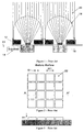
- FIG. 1 illustrates the operation of microlenses.
- a sensor 10 comprises circuitry portions 12 which overlie a substrate 14 which block incident light, meaning that the sensor is only sensitive to light at certain sensitive areas 16 of the substrate 14.
- a microlens 18 focuses incident light, represented by light rays 20, onto the sensitive areas 16.
- Microlenses are implemented on a large number of image sensors. They are distributed over the image array (one microlens per pixel). The technology to produce microlenses is commonly found in high-volume silicon manufacture.
- the microlens is formed by depositing a photoresist material on the surface of the sensor. It is patterned using photo-lithography (aligned to the pixel structure) and etched, resulting in a structure illustrated in Figs. 2 and 3.
- a grid of volume portions 22 are formed, having a width W1 and spaced apart by a distance S1.
- Fig. 3 shows a cross-section along A-A'. Each volume portion has a height H1.
- the microlenses are typically matched to the pitch of the sensor, i.e. the sensor pixel pitch is equal to S1+W1. Typically this 4pm - 10 ⁇ m.
- Figs. 4 and 5 illustrate the microlenses after being deformed by the heating process.
- Volume portions 22 have a width W2 and are spaced apart by a distance S2.
- Fig. 5 shows a cross-section along B-B'. Each volume portion 22 has a height H2.
- H1 will determine H2, from which the curvature and the focussing properties of the microlens are derived.
- the initial spacing between microlenses, S1 is critical. For construction of an efficient microlens, if S1 is too large, the light-collecting efficiency of the microlens will be reduced. However, if S1 is too small, two adjacent microlenses will touch and surface tension will prevent the microlens from forming correctly.
- adjacent in this context is taken to mean that two microlenses correspond to adjacent pixels on the array of the sensor. In practice, two microlenses may be considered as being “adjacent” if they are nearest neighbours and there is a risk of them merging when they deform under heat.
- S1 will ideally be as small as possible. However, for the formation of microlenses, practical values are 1 ⁇ m - 2 ⁇ m.
- microlens formation process can be "misused" to produce simple, but effective, 3-dimensional structures on the surface of the silicon. Instead of aiming to space the microlenses sufficiently far apart to prevent the merging of adjacent lenses, the microlens volume portions are deliberately formed close together so that they join up during reflow.
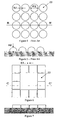
- Figs. 6-9 illustrate a first embodiment.
- photoresist volume portions 22 are spaced apart by a distance S3, where S3 ⁇ S1, and are formed in a defined shape, namely a ring.
- S3 is chosen to ensure that adjacent volume portions 22 merge together during reflow. S3 could even be made as low as zero.
- a reflow step is not necessary in order to ensure that a barrier of photoresist material is formed which can define a region suitable for constraining bio-optical reagents or analyte samples materials.
- a reflow step can still be performed to ensure that the edges and walls of the patterned regions and channels are smoother. The increased smoothness helps to reduce resistance to the flow of bio-optical reagent or analyte sample materials.
- FIG. 8 shows the result - there is an annulus 24 of microlens material with a void 26 in the middle.
- Fig. 9 shows a cross-section along line D-D' of Fig. 8.
- the annulus 24 has a width W3, with the void 26 having a dimension S4.
- the void 26 shown in Figs. 8 and 9 allows accurate deposition of the reagent during manufacture of a bio-optical sensor.
- the dimension S4 of this void 26 is independent of the width W3 of the microlens, but is usually an integral number of pixels. A typical value for W3 is 5 ⁇ m and for S4 is 50 ⁇ m.
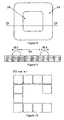
- Figs. 10 and 11 illustrate a second embodiment, where one microlens is omitted from the arrangement shown in Fig. 6. This produces an entrance 28 to the void 26, producing a "cup" shape.
- Figs. 10 and 11 show the microlens layouts before and after reflow.
- Figs. 12 and 13 show a third embodiment, for forming a channel 30.
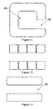
- FIG. 14 shows a fourth embodiment, where four annuli as shown in Fig. 6 are combined to form a microlens structure 32 comprising four sites 34.
- microlens material 32 provides an effective barrier between the sites, being hard and hard impervious to isolate reagent located in neighbouring sites 34. This sensor could then provide the sensing and/or detection of up to four different chemicals in the analyte.
- Fig. 15 shows a fifth embodiment, where two sites 36, 38 are connected by a channel 40. The connection allows the analyte to flow between different sites.
- the principles of the invention when applied to bio-optical sensor systems, allow both accurate deposition of a reagent during manufacture of the system and also the production of channels and guides to assist the flow of the analyte during operation of the system.
- the top surface of the sensor is usually formed from Silicon Nitride to protect the device.
- This material can also be patterned and etched to provide similar defined regions that serve similar purposes as described above.
- the invention sits well with existing manufacturing processes, and so it does not incur a cost penalty to introduce nor is its processing complex or time consuming. This reduces the overall cost of production of the sensors.
Landscapes
- Health & Medical Sciences (AREA)
- Engineering & Computer Science (AREA)
- Chemical & Material Sciences (AREA)
- Life Sciences & Earth Sciences (AREA)
- Physics & Mathematics (AREA)
- Immunology (AREA)
- General Physics & Mathematics (AREA)
- Hematology (AREA)
- Analytical Chemistry (AREA)
- General Health & Medical Sciences (AREA)
- Urology & Nephrology (AREA)
- Molecular Biology (AREA)
- Biomedical Technology (AREA)
- Manufacturing & Machinery (AREA)
- Optics & Photonics (AREA)
- Crystallography & Structural Chemistry (AREA)
- Biotechnology (AREA)
- Cell Biology (AREA)
- Microbiology (AREA)
- Chemical Kinetics & Catalysis (AREA)
- Clinical Laboratory Science (AREA)
- Food Science & Technology (AREA)
- Medicinal Chemistry (AREA)
- Biochemistry (AREA)
- Pathology (AREA)
- Solid State Image Pick-Up Elements (AREA)
Description
- The present invention relates to a method of forming a sensor.
- Bio-optical sensors are known, which detect photoemissive chemical reactions between an analyte and a reagent.
- Improved bio-optical sensors have a number of different reagents to enable them to detect the presence/concentration of several analytes. During the manufacture of such sensors, it is necessary to locate and separate the reagents, and during their operation, it is necessary to guide the sample containing the analyte over the sensor sites.
- Therefore, the sites must be mechanically isolated. It is known to pattern and etch suitable structures, either on the silicon of the sensor surface, or by making trenches in the silicon itself. However, these methods currently require special technology, processing and equipment which add to the cost of manufacture.
- When forming a structure on the surface of the sensor, materials such as polyimide are typically used, as they provide good patterning and etch properties. While found in the research laboratory, these chemicals are not usually found in the production environment. The introduction of these materials requires a modification to normal production processes.
- Prior known bio-optical sensors are known from
WO 00/33084 DE 10139742 to Freiburg University,US 6,159,681 andUS 2003/0064316 to Zebala et al , and the papers " Integrated Multi-Biosensors Based on an Ion-Sensitive Field-Effect Transistor Using Photolithographic Techniques", 8093 IEEE Transactions on Electron Devices 36(1989) July, no. 7 by Yoshio Hanazato et al, while a background document on microlenses is "Technique for monolithic fabrication of microlens arrays" by Zoran Popovic et al, 2219 Applied Optics 27(1988) 1 April, No. 7. - Therefore, there is a need for a method of forming 3D structures reliably and cheaply on the surface of sensor, the method ideally being easy to incorporate into existing manufacturing processes.
- According to a first aspect of the present invention, there is provided a method of forming a sensor as set out in the attached
claim 1. - Specific embodiments of the invention shall now be described, by way of example only, with reference to the accompanying drawings, in which:
- Fig. 1 shows the prior art structure and function of microlenses;
- Figs. 2 and 3 show plan and cross-sectional views of prior art microlenses before a reflow step is applied;
- Figs. 4 and 5 show plan and cross-sectional views of prior art microlenses after the reflow step is applied;
- Figs. 6 and 7 show plan and cross-sectional views of a first embodiment before a reflow step is applied;
- Figs. 8 and 9 show plan and cross-sectional views of the first embodiment after the reflow step is applied;
- Figs. 10 and 11 show plan views of a second embodiment before and after a reflow step is applied;
- Figs. 12 and 13 show plan views of a third embodiment before and after a reflow step is applied;
- Fig. 14 shows a plan view of a fourth embodiment ; and
- Fig. 15 shows a plan view of a fifth embodiment.
- It is known to incorporate microlenses on image sensors to overcome the sensitivity loss caused by the circuitry which blocks light. Fig. 1 illustrates the operation of microlenses. A
sensor 10 comprisescircuitry portions 12 which overlie asubstrate 14 which block incident light, meaning that the sensor is only sensitive to light at certainsensitive areas 16 of thesubstrate 14. To overcome the loss of light that would normally be blocked by thecircuitry 12, amicrolens 18 focuses incident light, represented bylight rays 20, onto thesensitive areas 16. - Microlenses are implemented on a large number of image sensors. They are distributed over the image array (one microlens per pixel). The technology to produce microlenses is commonly found in high-volume silicon manufacture.
- The microlens is formed by depositing a photoresist material on the surface of the sensor. It is patterned using photo-lithography (aligned to the pixel structure) and etched, resulting in a structure illustrated in Figs. 2 and 3. A grid of
volume portions 22 are formed, having a width W1 and spaced apart by a distance S1. Fig. 3 shows a cross-section along A-A'. Each volume portion has a height H1. - The microlenses are typically matched to the pitch of the sensor, i.e. the sensor pixel pitch is equal to S1+W1. Typically this 4pm - 10µm.
- The photoresist is then deformed by heating it until it melts, in what is referred to as a reflow process. This is carried out at a relatively low temperature (e.g. 200°C) - lower than the typical manufacturing temperature for the silicon, so the silicon is undamaged. When the microlens material melts, surface tension causes it to produce a hemisphere. Figs. 4 and 5 illustrate the microlenses after being deformed by the heating process.
Volume portions 22 have a width W2 and are spaced apart by a distance S2. Fig. 5 shows a cross-section along B-B'. Eachvolume portion 22 has a height H2. - During this process, the volume of and pitch between the microlenses remains unchanged. However, the shape and height does change, where W2>W1 and S2<S1.
- H1 will determine H2, from which the curvature and the focussing properties of the microlens are derived.
- The initial spacing between microlenses, S1, is critical. For construction of an efficient microlens, if S1 is too large, the light-collecting efficiency of the microlens will be reduced. However, if S1 is too small, two adjacent microlenses will touch and surface tension will prevent the microlens from forming correctly.
- The term "adjacent" in this context is taken to mean that two microlenses correspond to adjacent pixels on the array of the sensor. In practice, two microlenses may be considered as being "adjacent" if they are nearest neighbours and there is a risk of them merging when they deform under heat.
- S1 will ideally be as small as possible. However, for the formation of microlenses, practical values are 1µm - 2µm.
- The microlens formation process can be "misused" to produce simple, but effective, 3-dimensional structures on the surface of the silicon. Instead of aiming to space the microlenses sufficiently far apart to prevent the merging of adjacent lenses, the microlens volume portions are deliberately formed close together so that they join up during reflow.
- Figs. 6-9 illustrate a first embodiment. As seen in Fig. 6,
photoresist volume portions 22 are spaced apart by a distance S3, where S3<S1, and are formed in a defined shape, namely a ring. The value of S3 is chosen to ensure thatadjacent volume portions 22 merge together during reflow. S3 could even be made as low as zero. - When S3 is zero, a reflow step is not necessary in order to ensure that a barrier of photoresist material is formed which can define a region suitable for constraining bio-optical reagents or analyte samples materials. However, a reflow step can still be performed to ensure that the edges and walls of the patterned regions and channels are smoother. The increased smoothness helps to reduce resistance to the flow of bio-optical reagent or analyte sample materials.
- During the heating process the microlens material will melt. As the squares are close, under the influence of gravity, the material will touch and surface tension will cause them to join up. Fig. 8 shows the result - there is an
annulus 24 of microlens material with a void 26 in the middle. Fig. 9 shows a cross-section along line D-D' of Fig. 8. Theannulus 24 has a width W3, with the void 26 having a dimension S4. - The void 26 shown in Figs. 8 and 9 allows accurate deposition of the reagent during manufacture of a bio-optical sensor. The dimension S4 of this void 26 is independent of the width W3 of the microlens, but is usually an integral number of pixels. A typical value for W3 is 5µm and for S4 is 50µm.
- In addition to forming an annulus/void, the idea can be extended to produce other shapes.
- Figs. 10 and 11 illustrate a second embodiment, where one microlens is omitted from the arrangement shown in Fig. 6. This produces an
entrance 28 to the void 26, producing a "cup" shape. - Figs. 10 and 11 show the microlens layouts before and after reflow.
- Figs. 12 and 13 show a third embodiment, for forming a
channel 30. - More complex shapes can also be constructed. Fig. 14 shows a fourth embodiment, where four annuli as shown in Fig. 6 are combined to form a
microlens structure 32 comprising foursites 34. - With this structure, four different reagents could be deposited at each of the four
sites 34. Themicrolens material 32 provides an effective barrier between the sites, being hard and hard impervious to isolate reagent located in neighbouringsites 34. This sensor could then provide the sensing and/or detection of up to four different chemicals in the analyte. - Fig. 15 shows a fifth embodiment, where two
sites channel 40. The connection allows the analyte to flow between different sites. - It will be appreciated that the regions formed by the particular shapes and formations referred to above are only a very few of a large number of regions that can be formed using the techniques of the present invention, and the present invention is in no way to be considered as being limited to these particular regions.
- The principles of the invention, when applied to bio-optical sensor systems, allow both accurate deposition of a reagent during manufacture of the system and also the production of channels and guides to assist the flow of the analyte during operation of the system.
- It is also to be recognised that the top surface of the sensor is usually formed from Silicon Nitride to protect the device. This material can also be patterned and etched to provide similar defined regions that serve similar purposes as described above.
- The invention sits well with existing manufacturing processes, and so it does not incur a cost penalty to introduce nor is its processing complex or time consuming. This reduces the overall cost of production of the sensors.
- Various improvements and modifications may be made to the above without departing from the scope of the invention.
Claims (4)
- A method of forming a sensor, comprising the step of forming a barrier of photoresist material on a surface of the sensor, the barrier defining at least one region which is suitable for constraining a bio-optical reagent or analyte therein; wherein said step of forming a barrier comprises the steps of:depositing photoresist material on a surface of the sensor;patterning and etching the photoresist material so that a plurality of discrete photoresist material volumes are formed and are spaced apart by a distance, the value of which ensures that adjacent volumes coalesce upon heating; anddeforming the photoresist material by heating a plurality of the discrete material volumes such that adjacent volumes form the barrier
- The method of claim 1, wherein the distance is not more than 2µm.
- The method of claim 1 or claim 2, further comprising the step of depositing a bio-optical reagent in the region defined by the barrier.
- The method of claim 3, further comprising the step of depositing different types of reagents in different regions.
Priority Applications (3)
| Application Number | Priority Date | Filing Date | Title |
|---|---|---|---|
| EP03258136A EP1557717B1 (en) | 2003-12-22 | 2003-12-22 | Method of forming sensors comprising barriers of photoresist material |
| DE60315691T DE60315691D1 (en) | 2003-12-22 | 2003-12-22 | Method of producing sensors with barriers of photoresist material |
| US11/018,979 US7273633B2 (en) | 2003-12-22 | 2004-12-21 | Sensors |
Applications Claiming Priority (1)
| Application Number | Priority Date | Filing Date | Title |
|---|---|---|---|
| EP03258136A EP1557717B1 (en) | 2003-12-22 | 2003-12-22 | Method of forming sensors comprising barriers of photoresist material |
Publications (2)
| Publication Number | Publication Date |
|---|---|
| EP1557717A1 EP1557717A1 (en) | 2005-07-27 |
| EP1557717B1 true EP1557717B1 (en) | 2007-08-15 |
Family
ID=34626441
Family Applications (1)
| Application Number | Title | Priority Date | Filing Date |
|---|---|---|---|
| EP03258136A Expired - Lifetime EP1557717B1 (en) | 2003-12-22 | 2003-12-22 | Method of forming sensors comprising barriers of photoresist material |
Country Status (3)
| Country | Link |
|---|---|
| US (1) | US7273633B2 (en) |
| EP (1) | EP1557717B1 (en) |
| DE (1) | DE60315691D1 (en) |
Families Citing this family (9)
| Publication number | Priority date | Publication date | Assignee | Title |
|---|---|---|---|---|
| US20190357827A1 (en) | 2003-08-01 | 2019-11-28 | Dexcom, Inc. | Analyte sensor |
| US8774886B2 (en) | 2006-10-04 | 2014-07-08 | Dexcom, Inc. | Analyte sensor |
| EP1544602B1 (en) * | 2003-12-19 | 2008-05-07 | STMicroelectronics Limited | Bio-optical sensors |
| US7557338B2 (en) * | 2006-03-14 | 2009-07-07 | Avago Technologies General Ip (Singapore) Pte. Ltd. | Electronic device with integrated optical navigation module and microlens array therefore |
| KR20080024770A (en) * | 2006-09-14 | 2008-03-19 | 삼성전자주식회사 | Micro lens and its formation method |
| KR100808114B1 (en) * | 2007-07-18 | 2008-02-29 | (주)실리콘화일 | Diagnostic device and its manufacturing method |
| US8828201B2 (en) | 2009-07-02 | 2014-09-09 | Dexcom, Inc. | Analyte sensors and methods of manufacturing same |
| US9848809B2 (en) | 2011-04-15 | 2017-12-26 | Dexcom, Inc. | Advanced analyte sensor calibration and error detection |
| US20180199873A1 (en) | 2017-01-19 | 2018-07-19 | Dexcom, Inc. | Flexible analyte sensors |
Family Cites Families (6)
| Publication number | Priority date | Publication date | Assignee | Title |
|---|---|---|---|---|
| EP0368482A1 (en) * | 1988-10-14 | 1990-05-16 | Secretary Of State For Trade And Industry In Her Britannic Majesty's Gov. Of The U.K. Of Great Britain And Northern Ireland | Method of making a product with a feature having a multiplicity of fine lines |
| US6159681A (en) * | 1997-05-28 | 2000-12-12 | Syntrix Biochip, Inc. | Light-mediated method and apparatus for the regional analysis of biologic material |
| WO1999061653A2 (en) * | 1998-05-27 | 1999-12-02 | Syntrix Biochip | Light-mediated regional analysis of biologic material |
| WO2000033084A2 (en) * | 1998-12-01 | 2000-06-08 | Syntrix Biochip, Inc. | Arrays of organic compounds attached to surfaces |
| WO2000032678A1 (en) * | 1998-12-01 | 2000-06-08 | Syntrix Biochip, Inc. | Solvent resistant photosensitive compositions |
| DE10139742A1 (en) * | 2001-08-13 | 2003-03-06 | Univ Freiburg | Process for producing a "lab on chip" from photoresist material for medical diagnostic applications |
-
2003
- 2003-12-22 EP EP03258136A patent/EP1557717B1/en not_active Expired - Lifetime
- 2003-12-22 DE DE60315691T patent/DE60315691D1/en not_active Expired - Lifetime
-
2004
- 2004-12-21 US US11/018,979 patent/US7273633B2/en not_active Expired - Lifetime
Also Published As
| Publication number | Publication date |
|---|---|
| DE60315691D1 (en) | 2007-09-27 |
| US7273633B2 (en) | 2007-09-25 |
| EP1557717A1 (en) | 2005-07-27 |
| US20050151148A1 (en) | 2005-07-14 |
Similar Documents
| Publication | Publication Date | Title |
|---|---|---|
| US20250389888A1 (en) | Arrays of integrated analytical devices and methods for production | |
| US12196677B2 (en) | Arrays of integrated analytical devices | |
| RU2744399C1 (en) | Structure of imaging detector (variants) and method of generating thereof | |
| US8335029B2 (en) | Micromirror arrays having self aligned features | |
| US6906797B1 (en) | Side light activated microfluid channels | |
| KR101111231B1 (en) | Microwell array chip and its manufacturing method | |
| US20030186027A1 (en) | Micro-passage element used for fluid analysis | |
| US8026559B2 (en) | Biosensor devices and method for fabricating the same | |
| RU2016122443A (en) | BIOSENSORS FOR BIOLOGICAL OR CHEMICAL ANALYSIS AND METHODS FOR THEIR MANUFACTURE | |
| EP1557717A1 (en) | Sensors comprising barriers of photoresist material | |
| US20130052649A1 (en) | Multilayer high density microwells | |
| KR20180004480A (en) | Image Sensors Having a Plurality of Photodiodes Sharing One Color Filter and One Micro-lens | |
| EP4095516B1 (en) | Biosensor with grating array | |
| CN110579453A (en) | Sensing device and method for detecting fluorescence in a fluid containing biological material | |
| JP2009080313A (en) | Color filter, method for manufacturing the same, solid-state imaging device using the same, and method for manufacturing the same | |
| WO2001020309A1 (en) | Side light activated microfluid channels | |
| JP2010021184A (en) | Method for manufacturing infrared sensor element | |
| KR20100122534A (en) | Flexible biosensor, method for manufacturing and using the same | |
| US6667499B1 (en) | Solid-state image sensing device and method of manufacturing the same | |
| CN122057594A (en) | Detection substrate, preparation method thereof and microfluidic chip | |
| WO2013077576A1 (en) | Microfluidic semiconductor sensor |
Legal Events
| Date | Code | Title | Description |
|---|---|---|---|
| PUAI | Public reference made under article 153(3) epc to a published international application that has entered the european phase |
Free format text: ORIGINAL CODE: 0009012 |
|
| AK | Designated contracting states |
Kind code of ref document: A1 Designated state(s): AT BE BG CH CY CZ DE DK EE ES FI FR GB GR HU IE IT LI LU MC NL PT RO SE SI SK TR |
|
| AX | Request for extension of the european patent |
Extension state: AL LT LV MK |
|
| 17P | Request for examination filed |
Effective date: 20051230 |
|
| AKX | Designation fees paid |
Designated state(s): DE FR GB IT |
|
| GRAP | Despatch of communication of intention to grant a patent |
Free format text: ORIGINAL CODE: EPIDOSNIGR1 |
|
| RTI1 | Title (correction) |
Free format text: METHOD OF FORMING SENSORS COMPRISING BARRIERS OF PHOTORESIST MATERIAL |
|
| GRAS | Grant fee paid |
Free format text: ORIGINAL CODE: EPIDOSNIGR3 |
|
| GRAA | (expected) grant |
Free format text: ORIGINAL CODE: 0009210 |
|
| AK | Designated contracting states |
Kind code of ref document: B1 Designated state(s): DE FR GB IT |
|
| REG | Reference to a national code |
Ref country code: GB Ref legal event code: FG4D |
|
| REF | Corresponds to: |
Ref document number: 60315691 Country of ref document: DE Date of ref document: 20070927 Kind code of ref document: P |
|
| ET | Fr: translation filed | ||
| PLBE | No opposition filed within time limit |
Free format text: ORIGINAL CODE: 0009261 |
|
| STAA | Information on the status of an ep patent application or granted ep patent |
Free format text: STATUS: NO OPPOSITION FILED WITHIN TIME LIMIT |
|
| 26N | No opposition filed |
Effective date: 20080516 |
|
| PG25 | Lapsed in a contracting state [announced via postgrant information from national office to epo] |
Ref country code: DE Free format text: LAPSE BECAUSE OF FAILURE TO SUBMIT A TRANSLATION OF THE DESCRIPTION OR TO PAY THE FEE WITHIN THE PRESCRIBED TIME-LIMIT Effective date: 20071116 |
|
| PG25 | Lapsed in a contracting state [announced via postgrant information from national office to epo] |
Ref country code: IT Free format text: LAPSE BECAUSE OF NON-PAYMENT OF DUE FEES Effective date: 20071231 |
|
| PGFP | Annual fee paid to national office [announced via postgrant information from national office to epo] |
Ref country code: GB Payment date: 20101201 Year of fee payment: 8 |
|
| PGFP | Annual fee paid to national office [announced via postgrant information from national office to epo] |
Ref country code: FR Payment date: 20110120 Year of fee payment: 8 |
|
| GBPC | Gb: european patent ceased through non-payment of renewal fee |
Effective date: 20111222 |
|
| REG | Reference to a national code |
Ref country code: FR Ref legal event code: ST Effective date: 20120831 |
|
| PG25 | Lapsed in a contracting state [announced via postgrant information from national office to epo] |
Ref country code: GB Free format text: LAPSE BECAUSE OF NON-PAYMENT OF DUE FEES Effective date: 20111222 |
|
| PG25 | Lapsed in a contracting state [announced via postgrant information from national office to epo] |
Ref country code: FR Free format text: LAPSE BECAUSE OF NON-PAYMENT OF DUE FEES Effective date: 20120102 |