EP1557679A2 - High side current monitor - Google Patents
High side current monitor Download PDFInfo
- Publication number
- EP1557679A2 EP1557679A2 EP04257815A EP04257815A EP1557679A2 EP 1557679 A2 EP1557679 A2 EP 1557679A2 EP 04257815 A EP04257815 A EP 04257815A EP 04257815 A EP04257815 A EP 04257815A EP 1557679 A2 EP1557679 A2 EP 1557679A2
- Authority
- EP
- European Patent Office
- Prior art keywords
- current
- terminal
- transistor
- resistor
- voltage
- Prior art date
- Legal status (The legal status is an assumption and is not a legal conclusion. Google has not performed a legal analysis and makes no representation as to the accuracy of the status listed.)
- Granted
Links
Images



Classifications
-
- G—PHYSICS
- G01—MEASURING; TESTING
- G01R—MEASURING ELECTRIC VARIABLES; MEASURING MAGNETIC VARIABLES
- G01R19/00—Arrangements for measuring currents or voltages or for indicating presence or sign thereof
- G01R19/0023—Measuring currents or voltages from sources with high internal resistance by means of measuring circuits with high input impedance, e.g. OP-amplifiers
-
- G—PHYSICS
- G01—MEASURING; TESTING
- G01R—MEASURING ELECTRIC VARIABLES; MEASURING MAGNETIC VARIABLES
- G01R1/00—Details of instruments or arrangements of the types included in groups G01R5/00 - G01R13/00 and G01R31/00
- G01R1/20—Modifications of basic electric elements for use in electric measuring instruments; Structural combinations of such elements with such instruments
- G01R1/203—Resistors used for electric measuring, e.g. decade resistors standards, resistors for comparators, series resistors, shunts
-
- G—PHYSICS
- G01—MEASURING; TESTING
- G01R—MEASURING ELECTRIC VARIABLES; MEASURING MAGNETIC VARIABLES
- G01R19/00—Arrangements for measuring currents or voltages or for indicating presence or sign thereof
- G01R19/0092—Measuring current only
Definitions
- This invention relates to the field of current monitors, and particularly to "high side" current monitors.
- a high side current monitor is designed to measure the signal current through a sensing element connected in series with a circuit's high side (as opposed to its return side).
- a shunt voltage proportional to the signal current is developed across the sensing element - typically a small resistor.
- the current monitor measures the differential voltage across the sensing element, and produces a ground or common-referred output that varies with the sensed current.
- a conventional high side current monitor is shown in FIG. 1.
- a sensing element 10 here a resistor having a resistance R s
- R s is connected in series with a signal 12 having a voltage V1 and carries a current of interest I sense to a load 14; R s is typically on the order of 0.1 ⁇ .
- An operational amplifier A1 is connected across the sensing element, with its inverting input connected to the sensing element's load side, and its non-inverting input connected to the sensing element's high side via a resistor 15 having a resistance R1.
- a feedback transistor Q0 here a NPN, has its base connected to the output of A1, its collector connected to the junction of R1 and A1's non-inverting input, and its emitter providing an output I out .
- I out is delivered to an output resistor 16 having a resistance Rout to produce an output voltage V out .
- I sense develops a shunt voltage V sense across R s ; A1 responds by causing Q0 to conduct a current through R1 necessary to equalize A1's inverting and non-inverting inputs.
- This current (I out ) is proportional to the voltage (V sense ) across - and thus to the current (I sense ) through - sensing element 10.
- output voltage V out I out R out , it is also proportional to current of interest I sense .
- the differential voltage applied to A1 can have a large common mode potential.
- An op amp IC has an associated breakdown voltage determined by its fabrication process, which limits its common mode input range - which in turn limits the signals with which the current monitor of FIG. 1 can be safely used.
- a high side current monitor circuit is presented which overcomes the problems noted above.
- the present high side current monitor circuit includes components of the monitor described above: a sensing element is connected between high and load side terminals, carries a current of interest I sense , and develops a shunt voltage V sense between the terminals in response to I sense .
- An op amp's non-inverting input is coupled to the load side terminal, and a resistor is connected between the high side terminal and the amplifier's inverting input.
- a feedback transistor is connected to the op amp's output and conducts an output current I out through the resistor to a current output node necessary to make the voltages at the amp's inverting and non-inverting inputs equal - such that I out is proportional to I sense .
- the present current monitor circuit may also include an output load resistor connected between a second node and ground, and a second transistor coupled between the current output node and the second node and connected to conduct I out to the output load resistor such that a ground-referred voltage proportional to V sense is developed at the second node.
- the op amp and feedback transistor are preferably contained within an integrated circuit (IC) package, while the second transistor is preferably external to the IC and fabricated with a high voltage process. When so arranged, the external transistor stands off most of the common mode voltage, thereby reducing the voltage across the IC to less than the breakdown voltage associated with the IC's fabrication process. This permits measurement of shunt voltages having common mode voltages in excess of the breakdown voltage.
- the discrete transistor can be a P-type field-effect transistor (FET) or a PNP bipolar. If the latter, the invention preferably includes a base current recycling circuit which corrects for errors that would otherwise arise due to the external transistor's base current.
- FET field-effect transistor
- PNP bipolar P-type field-effect transistor
- the current monitor circuit may be configured as a "dual-use" IC, which can be used either with or without a discrete external transistor.
- the monitor circuit is further arranged such that it can be powered with a limited fraction of the common mode voltage when used with an external transistor, and is self-biased when used without an external transistor.
- FIG. 2 One embodiment of a high side current monitor circuit in accordance with the present invention is shown in FIG. 2.
- the circuit comprises a sensing element 10, typically a resistor having a resistance R s (though other devices having a known impedance could also be used), connected between high side and load side terminals 20 and 22 and in series with a signal 12 having a voltage V1.
- R s carries a current I sense to a load 14.
- Op amp A1 is connected across sensing element 10, with its non-inverting input coupled to load side terminal 22 and its inverting input connected to high side terminal 20 via a resistor 15 having a resistance R1.
- A1 may be powered between V1 and a local circuit common point (COM).
- COM local circuit common point
- the present monitor circuit can include a voltage limiter 23, which, when coupled to ground via a resistance R lim , enables A1 to be powered from a voltage much lower than the signal common mode voltage.
- a feedback transistor Q here a PNP bipolar (though a FET could also be used), has its base connected to the output of A1, its emitter connected to the junction (24) of R1 and A1's non-inverting input, and its collector providing an output current I out .
- I sense develops a shunt voltage V sense across R s ;
- A1 responds by causing Q1 to conduct current I out through R1 necessary to equalize A1's inverting and non-inverting inputs, such that I out is proportional to V sense and I sense .
- An op amp IC has an associated breakdown voltage determined by its fabrication process (referred to herein as the "process breakdown voltage"), which limits its common mode input range - which in turn limits the signals with which the current monitor circuit can be safely used.
- the invention overcomes this limitation with the addition of a transistor Q2, which is connected to conduct output current I out to output resistor 16, the other side of which is connected to ground.
- the voltage developed across resistor 16 is the circuit's output voltage V out .
- Components A1, Q1 and R1 are preferably housed within an IC 26, and Q2 is preferably a discrete transistor external to IC 26.
- the IC portion 26 can be biased so that most of the voltage between V1 and ground is stood off by transistor Q2, instead of being mostly across Q1 and A1 as in the prior art.
- Q2 is preferably made with a high voltage process, so that the monitor circuit can tolerate a V sense having a common mode voltage in excess of the process breakdown voltage.
- Voltage limiter 23 limits the voltage which can be made to appear across A1, and Q2 stands off most of the remaining common mode voltage - thereby enabling the measurement of a small shunt voltage (V sense ) having a common mode voltage in excess of the process breakdown voltage.
- Transistor Q2 is preferably a P-type FET (as shown in FIG. 2), or a PNP bipolar (described below and shown in FIG. 3). If a PFET is used, its gate should be connected to circuit common point COM , and the monitor circuit must be arranged such that the voltage between V1 and COM is sufficient to allow A1 to drive Q1 and for the collector of Q1 to drive Q2 to the gate-source voltage needed for Q2 to conduct I out to R out .
- the discrete external transistor is a PNP bipolar transistor
- the magnitude of I out conducted to output resistor 16 will be reduced by the PNP's base current, resulting in an error in V out .
- the invention preferably includes a base current recycling circuit to reduce or eliminate this error.
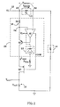
- a preferred arrangement is shown in FIG. 3.
- the discrete external transistor is a PNP bipolar transistor Q3.
- Q3's base is connected to a simple current mirror, made from transistor Q4 (diode-connected) and Q5, each of which is referenced to A1's circuit common point (COM).
- a resistor 30 having a resistance R2 approximately equal to R1 is interposed between load side terminal 22 and A1's non-inverting input, and the collector of Q5 is connected to the junction 32 of R2 and A1.
- Q3's base current I base biases Q4 so that its base voltage biases Q5 such that Q5 conducts a current I Q5 nearly equal to I base (assuming a 1:1 mirror).
- Current I Q5 is conducted through resistance R2.
- the component of voltage that results from this displaces A1's non-inverting input by a small amount.
- A1 responds by driving the base of Q1 to force a similar displacement across R1. This adds an increment of current to the signal current in R1, thereby increasing I out .
- the increment of current added to the signal current should closely approximate the base current I base , thereby correcting for the error that would otherwise arise due to Q3's base current.
- the present current monitor circuit is suitably configured as a "dual-use" IC, which can be used when the common mode potential of V sense is greater than or less than the process breakdown voltage.
- IC 40 is shown employed in its two uses in FIGs. 4A and 4B.
- IC 40 is connected to high side terminal 20 and load side terminal 22 via I/O pins VP and VSENS, respectively, which are also connected to resistors 15 and 30.
- the common mode potential of V sense is expected to be less than the process breakdown voltage. In this case, there is no need for an external discrete transistor to stand off the voltage across A1, so output current I out is connected directly to output resistor 16 (via an I/O pin IOUT) to generate V out .
- IC 40 preferably includes circuitry which allows it to be self-biased when the common mode potential of V sense is within the IC's safe operating range; one possible embodiment of such circuitry is shown in FIG. 4A.
- a voltage limiter 23 connected between V1 and COM provides A1's operating voltage; A1's operating current is set with a current I bias generated with a bias circuit 44.
- Bias circuit 44 preferably comprises a PNP transistor Q6 having its emitter connected to COM and voltage limiter 23, and a PNP transistor Q7 having its base and emitter connected in common with the base and emitter of Q6 .
- the collector of Q6 is connected to the collector of an NPN transistor Q8 at a node 45, and the collector and base of Q7 are connected to the emitter of a PNP transistor Q9.
- the base of Q9 is connected to node 45, and Q9's collector is connected to the collector of a diode-connected NPN transistor Q10 having its base connected in common with the base of Q8 and its emitter connected to Q8's emitter via an emitter degeneration resistor 46.
- a resistor 47 is connected between Q7's base and Q9's collector, and a resistor 48 is connected between the emitter and base of Q6/Q7.
- the bias circuit is connected to an I/O pin BIAS at Q10's emitter.
- resistor 46 in the emitter circuit of Q8 makes the emitter voltages of Q8 and Q10 different.
- Q8 is made larger than Q10 (8 times larger in FIG. 4A), so that in the absence of resistor 48, the Wilson current mirror composed of Q6, Q7, and Q9 could force Q10 to operate at the same current as Q8.
- Q8 and Q10 would operate at a fixed current density ratio of 8, causing a voltage (kT/q)ln8 ⁇ 54mV at room temperature to appear across resistor 46.
- This known temperature proportional voltage determines the magnitude of the equal currents in inverse proportion to resistor 46.
- bias current I bias would be the sum of the equal proportional-to-absolute-temperature (PTAT) currents in Q8 and Q10.
- PTAT proportional-to-absolute-temperature
- Adding resistor 48 provides an additional component of current in Q9 since it must drive resistor 48 until the voltage across it makes the base-emitter voltage for Q6. This current complements the PTAT current with a complementary-to-absolute-temperature (CTAT) current so that the total bias current is nearly temperature-invariant.
- CTAT complementary-to-absolute-temperature
- Bias circuit 44 should be arranged to provide an I bias having a magnitude sufficient to operate the IC, but no more than the voltage limiter's maximum allowable current.
- the voltage limiter is preferably arranged to stabilize A1's operating voltage near the minimum that it needs.
- the present current monitor may be used as a stand-alone IC for use in low voltage applications, or in an extended voltage application by adding an external discrete transistor (Q2/Q3) and a resistor (52).
- the invention further enables the IC to be fabricated using a basic low voltage process.
- bias circuit implementation shown in FIGs. 4A and 4B is preferred, many other circuits could be employed to establish appropriate operating points for IC 40.
- voltage limiter 23 could be implemented in many different ways. For example, a zener diode (as shown in FIGs. 2-4) or an avalanche breakdown diode could be used. Another possibility is to use an electronic bandgap shunt regulator; one possible embodiment of such a regulator is shown in FIG. 5.
Landscapes
- Physics & Mathematics (AREA)
- General Physics & Mathematics (AREA)
- Measurement Of Current Or Voltage (AREA)
- Control Of Electrical Variables (AREA)
- Measurement Of Radiation (AREA)
- Analysing Materials By The Use Of Radiation (AREA)
- Other Investigation Or Analysis Of Materials By Electrical Means (AREA)
Abstract
Description
Claims (27)
- A high side current monitor circuit, comprising:a high side terminal (20);a load side terminal (22);a current sensing element (10) connected between said high and load side terminals which carries a current of interest Isense and which develops a shunt voltage Vsense between said high side and load side terminals in response to Isense, said shunt voltage having a common mode voltage Vcm with respect to a ground terminal;an operational amplifier (A1) , said amplifier's non-inverting input coupled to said load side terminal;a first resistor (15) connected between said high side terminal and said amplifier's inverting input;a first transistor (Q1) having a control input and a current circuit, said control input connected to the output of said amplifier and said current circuit connected between said inverting input and a current output node such that said first transistor conducts an output current Iout through said first resistor to said current output node necessary to make the voltages at said inverting and non-inverting inputs equal such that Iout is proportional to Isense;an output load resistor (16) connected between a second node (Vout) and said ground terminal; anda second transistor (Q2) coupled between said current output node and said second node and connected to conduct said output current to said load resistor such that a voltage proportional to Isense and referred to said ground terminal is developed at said second node.
- The current monitor circuit of claim 1, wherein said amplifier, first resistor and first transistor comprise an integrated circuit (IC) having an associated process breakdown voltage, said second transistor and said output load resistor standing off a substantial portion of said common mode voltage such that the common mode voltage to which said IC is subjected is less than said process breakdown voltage.
- The current monitor circuit of claim 2, wherein said amplifier is operated with an operating voltage referred to a common terminal (COM) and said second transistor is a P-type field-effect transistor (PFET) having its source connected to said current output node, its drain connected to said second node, and its gate connected to said common terminal.
- The current monitor circuit of claim 2, wherein said second transistor is a PNP bipolar transistor having its emitter connected to said current output node and its collector connected to said second node, said current monitor circuit further comprising a base current recycling circuit arranged to cause the current in said first resistor to be incremented by an amount approximately equal to said second transistor's base current.
- The current monitor circuit of claim 4, wherein said base current recycling circuit comprises:a third resistor (30) interposed between said load side terminal and said amplifier's non-inverting input and having a resistance approximately equal to that of said first resistor; anda current mirror (Q4,Q5) connected to the base of said second transistor and to said amplifier's non-inverting input such that said second transistor's base current is mirrored to said amplifier's non-inverting input and said mirrored current flows through said third resistor, such that said amplifier increments the current in said first resistor and thereby in Iout by an amount approximately equal to said base current to equalize the voltages at its inverting and non-inverting inputs.
- The current monitor circuit of claim 1, further comprising a voltage limiter (23) coupled between said high side terminal and said common terminal which establishes an operating voltage for said amplifier and enables said amplifier to be powered from a voltage lower than Vcm.
- The current monitor circuit of claim 6, further comprising a bias current source (44) coupled to said common terminal which provides an operating current (Ibias) for said amplifier.
- The current monitor circuit of claim 7, wherein said bias current source comprises a resistor (52) connected between said common terminal and said ground terminal.
- The current monitor circuit of claim 7, wherein said bias current source is a bias circuit comprising:a first PNP transistor (Q6) having its emitter coupled to said common terminal;a second PNP transistor (Q7) having its emitter connected to the emitter of said first PNP transistor, and its base and collector connected to the base of said first PNP transistor;a second resistor (48) connected between the common bases and common emitters of said first and second PNP transistors;a first NPN transistor (Q10) having its emitter connected to a bias terminal, said first NPN transistor diode-connected;a second NPN transistor (Q8) having its base connected to the base of said first NPN transistor;a third resistor (46) connected between the emitters of said first and second NPN transistors;a fourth resistor (47) connected between the base of said second PNP transistor and the collector of said first NPN transistor; anda third PNP transistor (Q9) having its emitter connected to the collector of said second PNP transistor, its collector connected to the collector of said first NPN transistor, and its base connected to the collector of said second NPN transistor;the emitter of said second NPN transistor being larger than the emitter of said first NPN transistor.
- The current monitor circuit of claim 9, wherein said bias terminal is connected to said ground terminal such that said bias circuit provides said bias current to said common terminal.
- The current monitor circuit of 6, wherein said voltage limiter comprises a zener diode.
- The current monitor circuit of 6, wherein said voltage limiter comprises an avalanche breakdown diode.
- The current monitor circuit of 6, wherein said voltage limiter comprises a bandgap shunt regulator.
- A dual-use integrated circuit (IC) high side current monitor circuit suitable for use in measuring currents of interest having common mode voltages either above or below a predetermined process breakdown voltage, said IC comprising:a high side terminal (20);a load side terminal (22), said high and load side terminals suitable for connection across a current sensing element (10) which carries a current of interest Isense and which develops a shunt voltage Vsense between said high side and load side terminals in response to Isense, said shunt voltage having a common mode voltage Vcm with respect to an external ground terminal;an operational amplifier (A1) operated with an operating voltage referred to an IC common terminal (COM), said amplifier having an associated breakdown voltage;a first resistor (15) connected between said high side terminal and said amplifier's inverting input;a second resistor (30) connected between said load side terminal and said amplifier's non-inverting input, said second resistor having a resistance approximately equal to that of said first resistor;a first transistor (Q1) having a control input and a current circuit, said control input connected to the output of said amplifier and said current circuit connected between said inverting input and a current output terminal such that said first transistor conducts an output current Iout through said first resistor to said current output terminal necessary to make the voltages at said inverting and non-inverting inputs equal such that Iout is proportional to Isense;a base current recycling circuit (Q4,Q5) comprising an alpha terminal and arranged to cause the current in said first resistor to be incremented by an amount approximately equal to a current conducted at said alpha terminal;a voltage limiter (23) coupled between said high side terminal and said IC common terminal which establishes an operating voltage and provides operating current for said amplifier, said operating current varying with a bias current (Ibias) applied to said IC at said common terminal; anda bias circuit (44) coupled between said common terminal and a bias terminal (BIAS) and arranged to provide said bias current to said common terminal when enabled.
- The dual-use IC of claim 14, further comprising:an output load resistor (16) external to said IC connected between a second node (Vout) and said external ground terminal; anda second transistor (Q3) external to said IC coupled between said current output terminal and said second node and connected to conduct said output current to said load resistor such that a ground-referred voltage proportional to Isense is developed at said second node,said second transistor and said output load resistor standing off a substantial portion of said common mode voltage such that the common mode voltage to which said IC is subjected is less than said process breakdown voltage.
- The dual-use IC of claim 15, wherein said second transistor is a P-type field-effect transistor (PFET) having its source connected to said current output node, its drain connected to said second node, and its gate connected to said IC common terminal.
- The dual-use IC of claim 15, wherein said second transistor is a PNP bipolar transistor having its emitter connected to said current output node, its collector connected to said second node, and its base connected to said alpha terminal, such that the current in said first resistor is incremented by an amount approximately equal to said second transistor's base current.
- The dual-use IC of claim 15, wherein said base current recycling circuit comprises a current mirror connected to an "alpha" terminal and to said amplifier's non-inverting input such that a current conducted at said alpha terminal is mirrored to said amplifier's non-inverting input and said mirrored current flows through said second resistor, such that said amplifier increments the current in said first resistor by an amount approximately equal to said current conducted at said alpha terminal.
- The dual-use IC of claim 14, wherein said bias circuit comprises:a first PNP transistor (Q6) having its emitter coupled to said common terminal;a second PNP transistor (Q7) having its emitter connected to the emitter of said first PNP transistor, and its base and collector connected to the base of said first PNP transistor;a third resistor (48) connected between the common bases and common emitters of said first and second PNP transistors;a first NPN transistor (Q10) having its emitter connected to said bias terminal, said first NPN transistor diode-connected;a second NPN transistor (Q8) having its base connected to the base of said first NPN transistor;a fourth resistor (46) connected between the emitters of said first and second NPN transistors;a fifth resistor (47) connected between the base of said second PNP transistor and the collector of said first NPN transistor; anda third PNP transistor (Q9) having its emitter connected to the collector of said second PNP transistor, its collector connected to the collector of said first NPN transistor, and its base connected to the collector of said second NPN transistor;the emitter of said second NPN transistor being larger than the emitter of said first NPN transistor.
- The dual-use IC of claim 19, wherein said bias terminal is connected to said ground terminal such that said bias circuit is enabled and provides said bias current to said common terminal.
- The dual-use IC of claim 19, wherein said bias terminal is connected to said common terminal such that said bias circuit is disabled, further comprising a resistor (52) connected between said bias and common terminals and said ground terminal such that said resistor provides said bias current to said common terminal.
- The dual-use IC of claim 19, further comprising:an output load resistor (16) external to said IC connected between a second node and said external ground terminal; anda second transistor (Q3) external to said IC coupled between said current output terminal and said second node and connected to conduct said output current to said load resistor such that a ground-referred voltage proportional to Isense is developed at said second node,said second transistor and said output load resistor standing off a substantial portion of said common mode voltage such that the common mode voltage to which said IC is subjected is less than said process breakdown voltage;said bias terminal connected to said common terminal such that said bias circuit is disabled, further comprising a resistor connected between said bias and common terminals and said ground terminal such that said resistor provides said bias current to said common terminal.
- The dual-use IC of claim 19, further comprising an output load resistor (16) external to said IC connected between said current output terminal and said external ground terminal such that a ground-referred voltage proportional to Isense is developed at said current output terminal, said bias terminal connected to said ground terminal such that said bias circuit is enabled and provides said bias current to said common terminal.
- The dual-use IC of claim 14, further comprising an output load resistor (16) external to said IC connected between said current output terminal and said external ground terminal such that a ground-referred voltage proportional to Isense is developed at said current output terminal.
- The dual-use IC of claim 14, wherein said voltage limiter comprises a zener diode.
- The dual-use IC of claim 14, wherein said voltage limiter comprises an avalanche breakdown diode.
- The dual-use IC of claim 14, wherein said voltage limiter comprises a bandgap shunt regulator.
Applications Claiming Priority (2)
| Application Number | Priority Date | Filing Date | Title |
|---|---|---|---|
| US10/762,647 US6956727B1 (en) | 2004-01-21 | 2004-01-21 | High side current monitor with extended voltage range |
| US762647 | 2004-01-21 |
Publications (3)
| Publication Number | Publication Date |
|---|---|
| EP1557679A2 true EP1557679A2 (en) | 2005-07-27 |
| EP1557679A3 EP1557679A3 (en) | 2005-11-02 |
| EP1557679B1 EP1557679B1 (en) | 2007-09-05 |
Family
ID=34634597
Family Applications (1)
| Application Number | Title | Priority Date | Filing Date |
|---|---|---|---|
| EP04257815A Expired - Lifetime EP1557679B1 (en) | 2004-01-21 | 2004-12-15 | High side current monitor |
Country Status (4)
| Country | Link |
|---|---|
| US (1) | US6956727B1 (en) |
| EP (1) | EP1557679B1 (en) |
| AT (1) | ATE372520T1 (en) |
| DE (1) | DE602004008734T2 (en) |
Cited By (3)
| Publication number | Priority date | Publication date | Assignee | Title |
|---|---|---|---|---|
| GB2447955A (en) * | 2007-03-29 | 2008-10-01 | Absl Power Solutions Ltd | High side current measurement |
| WO2008116747A1 (en) * | 2007-03-26 | 2008-10-02 | Robert Bosch Gmbh | Control circuit and control method for a piezoelectric element |
| WO2009020566A1 (en) * | 2007-08-06 | 2009-02-12 | Analog Devices, Inc. | Voltage transformation circuit |
Families Citing this family (33)
| Publication number | Priority date | Publication date | Assignee | Title |
|---|---|---|---|---|
| US8049573B2 (en) * | 2004-06-03 | 2011-11-01 | Silicon Laboratories Inc. | Bidirectional multiplexed RF isolator |
| US7902627B2 (en) | 2004-06-03 | 2011-03-08 | Silicon Laboratories Inc. | Capacitive isolation circuitry with improved common mode detector |
| US7460604B2 (en) | 2004-06-03 | 2008-12-02 | Silicon Laboratories Inc. | RF isolator for isolating voltage sensing and gate drivers |
| US7737871B2 (en) | 2004-06-03 | 2010-06-15 | Silicon Laboratories Inc. | MCU with integrated voltage isolator to provide a galvanic isolation between input and output |
| US7302247B2 (en) * | 2004-06-03 | 2007-11-27 | Silicon Laboratories Inc. | Spread spectrum isolator |
| US8441325B2 (en) | 2004-06-03 | 2013-05-14 | Silicon Laboratories Inc. | Isolator with complementary configurable memory |
| US8198951B2 (en) | 2004-06-03 | 2012-06-12 | Silicon Laboratories Inc. | Capacitive isolation circuitry |
| US7738568B2 (en) | 2004-06-03 | 2010-06-15 | Silicon Laboratories Inc. | Multiplexed RF isolator |
| US8169108B2 (en) * | 2004-06-03 | 2012-05-01 | Silicon Laboratories Inc. | Capacitive isolator |
| US7421028B2 (en) | 2004-06-03 | 2008-09-02 | Silicon Laboratories Inc. | Transformer isolator for digital power supply |
| US7447492B2 (en) * | 2004-06-03 | 2008-11-04 | Silicon Laboratories Inc. | On chip transformer isolator |
| US7577223B2 (en) | 2004-06-03 | 2009-08-18 | Silicon Laboratories Inc. | Multiplexed RF isolator circuit |
| US7376212B2 (en) | 2004-06-03 | 2008-05-20 | Silicon Laboratories Inc. | RF isolator with differential input/output |
| US7821428B2 (en) | 2004-06-03 | 2010-10-26 | Silicon Laboratories Inc. | MCU with integrated voltage isolator and integrated galvanically isolated asynchronous serial data link |
| US7336122B2 (en) * | 2005-12-06 | 2008-02-26 | Supertex, Inc. | Low power high side current monitor which operates at high voltages and method therefor |
| US7928662B2 (en) * | 2006-12-18 | 2011-04-19 | Microsemi Corp.—Analog Mixed Signal Group Ltd. | Voltage range extender mechanism |
| US7570114B2 (en) * | 2007-07-24 | 2009-08-04 | Analog Devices, Inc. | Common mode rejection calibration method for difference amplifiers |
| JP5473531B2 (en) * | 2009-10-22 | 2014-04-16 | ラピスセミコンダクタ株式会社 | Bias potential generator |
| US8264216B2 (en) | 2010-09-21 | 2012-09-11 | Sendyne Corp. | High-accuracy low-power current sensor with large dynamic range |
| US8451032B2 (en) | 2010-12-22 | 2013-05-28 | Silicon Laboratories Inc. | Capacitive isolator with schmitt trigger |
| WO2012117275A2 (en) | 2011-03-01 | 2012-09-07 | Sendyne Corp. | Current sensor |
| JP5920088B2 (en) * | 2012-07-24 | 2016-05-18 | コニカミノルタ株式会社 | Current detection circuit and ultrasonic diagnostic apparatus using current detection circuit |
| US8902005B2 (en) | 2012-09-25 | 2014-12-02 | Analog Devices, Inc. | Apparatus and method for wide common mode difference |
| US9264002B2 (en) | 2014-02-19 | 2016-02-16 | Analog Devices Global | Apparatus and methods for improving common mode rejection ratio |
| US9729140B2 (en) | 2014-03-05 | 2017-08-08 | Analog Devices, Inc. | Circuits with floating bias |
| US9496835B2 (en) | 2014-12-15 | 2016-11-15 | Semiconductor Components Industries, Llc | Current sense amplifer with extended common mode input voltage range |
| US9960741B2 (en) | 2016-06-27 | 2018-05-01 | Dialog Semiconductor (Uk) Limited | High frequency common mode rejection technique for large dynamic common mode signals |
| EP3293888B1 (en) | 2016-09-13 | 2020-08-26 | Allegro MicroSystems, LLC | Signal isolator having bidirectional communication between die |
| US11115244B2 (en) | 2019-09-17 | 2021-09-07 | Allegro Microsystems, Llc | Signal isolator with three state data transmission |
| EP3812873B1 (en) * | 2019-10-24 | 2025-02-26 | NXP USA, Inc. | Voltage reference generation with compensation for temperature variation |
| CN114755469B (en) * | 2020-12-28 | 2025-04-22 | 致茂电子股份有限公司 | Electronic load equipment |
| JP2022111592A (en) * | 2021-01-20 | 2022-08-01 | キオクシア株式会社 | semiconductor integrated circuit |
| CN113219233B (en) * | 2021-04-30 | 2023-06-09 | 石家庄宇飞电子有限公司 | Voltage expansion circuit for high-side current sampling |
Family Cites Families (6)
| Publication number | Priority date | Publication date | Assignee | Title |
|---|---|---|---|---|
| DE4101492A1 (en) * | 1991-01-19 | 1992-07-23 | Telefunken Electronic Gmbh | Power current circuitry e.g. for DC motor - uses controllable resistor in branch circuit to detect load current regulated in output stage |
| US5220207A (en) * | 1991-09-03 | 1993-06-15 | Allegro Microsystems, Inc. | Load current monitor for MOS driver |
| US6222922B1 (en) * | 1997-04-22 | 2001-04-24 | Silicon Laboratories, Inc. | Loop current monitor circuitry and method for a communication system |
| JP3101998B2 (en) * | 1997-06-26 | 2000-10-23 | 富士電機株式会社 | Overcurrent detection circuit |
| JP3393203B2 (en) * | 1999-09-13 | 2003-04-07 | 株式会社ホンダエレシス | Inspection method of current detection circuit |
| US6785521B2 (en) * | 2001-03-21 | 2004-08-31 | Ericsson Inc. | System and method for current-mode amplitude modulation |
-
2004
- 2004-01-21 US US10/762,647 patent/US6956727B1/en not_active Expired - Lifetime
- 2004-12-15 AT AT04257815T patent/ATE372520T1/en not_active IP Right Cessation
- 2004-12-15 EP EP04257815A patent/EP1557679B1/en not_active Expired - Lifetime
- 2004-12-15 DE DE602004008734T patent/DE602004008734T2/en not_active Expired - Lifetime
Cited By (4)
| Publication number | Priority date | Publication date | Assignee | Title |
|---|---|---|---|---|
| WO2008116747A1 (en) * | 2007-03-26 | 2008-10-02 | Robert Bosch Gmbh | Control circuit and control method for a piezoelectric element |
| GB2447955A (en) * | 2007-03-29 | 2008-10-01 | Absl Power Solutions Ltd | High side current measurement |
| WO2009020566A1 (en) * | 2007-08-06 | 2009-02-12 | Analog Devices, Inc. | Voltage transformation circuit |
| US7821245B2 (en) | 2007-08-06 | 2010-10-26 | Analog Devices, Inc. | Voltage transformation circuit |
Also Published As
| Publication number | Publication date |
|---|---|
| DE602004008734T2 (en) | 2008-06-12 |
| EP1557679B1 (en) | 2007-09-05 |
| EP1557679A3 (en) | 2005-11-02 |
| US6956727B1 (en) | 2005-10-18 |
| DE602004008734D1 (en) | 2007-10-18 |
| ATE372520T1 (en) | 2007-09-15 |
Similar Documents
| Publication | Publication Date | Title |
|---|---|---|
| US6956727B1 (en) | High side current monitor with extended voltage range | |
| US10222819B2 (en) | Fractional bandgap reference voltage generator | |
| CA2068219C (en) | Regulated bifurcated power supply | |
| EP1174720B1 (en) | Current sensing circuit | |
| US4792748A (en) | Two-terminal temperature-compensated current source circuit | |
| US6492845B1 (en) | Low voltage current sense amplifier circuit | |
| US9459647B2 (en) | Bandgap reference circuit and bandgap reference current source with two operational amplifiers for generating zero temperature correlated current | |
| US8269478B2 (en) | Two-terminal voltage regulator with current-balancing current mirror | |
| US6011413A (en) | Structure of current measuring circuit | |
| EP3926437B1 (en) | A high accuracy zener based voltage reference circuit | |
| US6466422B2 (en) | Current limit protection circuit for a voltage regulator | |
| JPH02285408A (en) | Band gap voltage reference with advanced temperature correction | |
| US6181196B1 (en) | Accurate bandgap circuit for a CMOS process without NPN devices | |
| JP2002304224A (en) | Circuit and method for generating voltage | |
| EP2905672A1 (en) | An apparatus and method for a modified brokaw bandgap reference circuit for improved low voltage power supply | |
| EP3929694B1 (en) | A voltage regulator | |
| US5621307A (en) | Fast recovery temperature compensated reference source | |
| US8278995B1 (en) | Bandgap in CMOS DGO process | |
| US6465998B2 (en) | Current source with low supply voltage and with low voltage sensitivity | |
| EP2804067A1 (en) | Low output noise density low power ldo voltage regulator | |
| US6995588B2 (en) | Temperature sensor apparatus | |
| US20120153997A1 (en) | Circuit for Generating a Reference Voltage Under a Low Power Supply Voltage | |
| US6583611B2 (en) | Circuit generator of a voltage signal which is independent of temperature and has low sensitivity to variations in process parameters | |
| EP1439445B1 (en) | Temperature compensated bandgap voltage reference | |
| US6501254B2 (en) | Voltage source |
Legal Events
| Date | Code | Title | Description |
|---|---|---|---|
| PUAI | Public reference made under article 153(3) epc to a published international application that has entered the european phase |
Free format text: ORIGINAL CODE: 0009012 |
|
| AK | Designated contracting states |
Kind code of ref document: A2 Designated state(s): AT BE BG CH CY CZ DE DK EE ES FI FR GB GR HU IE IS IT LI LT LU MC NL PL PT RO SE SI SK TR |
|
| AX | Request for extension of the european patent |
Extension state: AL BA HR LV MK YU |
|
| PUAL | Search report despatched |
Free format text: ORIGINAL CODE: 0009013 |
|
| AK | Designated contracting states |
Kind code of ref document: A3 Designated state(s): AT BE BG CH CY CZ DE DK EE ES FI FR GB GR HU IE IS IT LI LT LU MC NL PL PT RO SE SI SK TR |
|
| AX | Request for extension of the european patent |
Extension state: AL BA HR LV MK YU |
|
| 17P | Request for examination filed |
Effective date: 20060510 |
|
| AKX | Designation fees paid |
Designated state(s): AT BE BG CH CY CZ DE DK EE ES FI FR GB GR HU IE IS IT LI LT LU MC NL PL PT RO SE SI SK TR |
|
| 17Q | First examination report despatched |
Effective date: 20060906 |
|
| GRAP | Despatch of communication of intention to grant a patent |
Free format text: ORIGINAL CODE: EPIDOSNIGR1 |
|
| GRAS | Grant fee paid |
Free format text: ORIGINAL CODE: EPIDOSNIGR3 |
|
| GRAA | (expected) grant |
Free format text: ORIGINAL CODE: 0009210 |
|
| AK | Designated contracting states |
Kind code of ref document: B1 Designated state(s): AT BE BG CH CY CZ DE DK EE ES FI FR GB GR HU IE IS IT LI LT LU MC NL PL PT RO SE SI SK TR |
|
| REG | Reference to a national code |
Ref country code: GB Ref legal event code: FG4D |
|
| REG | Reference to a national code |
Ref country code: CH Ref legal event code: EP |
|
| REF | Corresponds to: |
Ref document number: 602004008734 Country of ref document: DE Date of ref document: 20071018 Kind code of ref document: P |
|
| REG | Reference to a national code |
Ref country code: IE Ref legal event code: FG4D |
|
| ET | Fr: translation filed | ||
| PG25 | Lapsed in a contracting state [announced via postgrant information from national office to epo] |
Ref country code: ES Free format text: LAPSE BECAUSE OF FAILURE TO SUBMIT A TRANSLATION OF THE DESCRIPTION OR TO PAY THE FEE WITHIN THE PRESCRIBED TIME-LIMIT Effective date: 20071216 Ref country code: LT Free format text: LAPSE BECAUSE OF FAILURE TO SUBMIT A TRANSLATION OF THE DESCRIPTION OR TO PAY THE FEE WITHIN THE PRESCRIBED TIME-LIMIT Effective date: 20070905 Ref country code: FI Free format text: LAPSE BECAUSE OF FAILURE TO SUBMIT A TRANSLATION OF THE DESCRIPTION OR TO PAY THE FEE WITHIN THE PRESCRIBED TIME-LIMIT Effective date: 20070905 |
|
| PG25 | Lapsed in a contracting state [announced via postgrant information from national office to epo] |
Ref country code: AT Free format text: LAPSE BECAUSE OF FAILURE TO SUBMIT A TRANSLATION OF THE DESCRIPTION OR TO PAY THE FEE WITHIN THE PRESCRIBED TIME-LIMIT Effective date: 20070905 Ref country code: PL Free format text: LAPSE BECAUSE OF FAILURE TO SUBMIT A TRANSLATION OF THE DESCRIPTION OR TO PAY THE FEE WITHIN THE PRESCRIBED TIME-LIMIT Effective date: 20070905 Ref country code: LI Free format text: LAPSE BECAUSE OF FAILURE TO SUBMIT A TRANSLATION OF THE DESCRIPTION OR TO PAY THE FEE WITHIN THE PRESCRIBED TIME-LIMIT Effective date: 20070905 Ref country code: CH Free format text: LAPSE BECAUSE OF FAILURE TO SUBMIT A TRANSLATION OF THE DESCRIPTION OR TO PAY THE FEE WITHIN THE PRESCRIBED TIME-LIMIT Effective date: 20070905 |
|
| NLV1 | Nl: lapsed or annulled due to failure to fulfill the requirements of art. 29p and 29m of the patents act | ||
| PG25 | Lapsed in a contracting state [announced via postgrant information from national office to epo] |
Ref country code: BE Free format text: LAPSE BECAUSE OF FAILURE TO SUBMIT A TRANSLATION OF THE DESCRIPTION OR TO PAY THE FEE WITHIN THE PRESCRIBED TIME-LIMIT Effective date: 20070905 |
|
| REG | Reference to a national code |
Ref country code: CH Ref legal event code: PL |
|
| PG25 | Lapsed in a contracting state [announced via postgrant information from national office to epo] |
Ref country code: NL Free format text: LAPSE BECAUSE OF FAILURE TO SUBMIT A TRANSLATION OF THE DESCRIPTION OR TO PAY THE FEE WITHIN THE PRESCRIBED TIME-LIMIT Effective date: 20070905 Ref country code: GR Free format text: LAPSE BECAUSE OF FAILURE TO SUBMIT A TRANSLATION OF THE DESCRIPTION OR TO PAY THE FEE WITHIN THE PRESCRIBED TIME-LIMIT Effective date: 20071206 |
|
| PG25 | Lapsed in a contracting state [announced via postgrant information from national office to epo] |
Ref country code: PT Free format text: LAPSE BECAUSE OF FAILURE TO SUBMIT A TRANSLATION OF THE DESCRIPTION OR TO PAY THE FEE WITHIN THE PRESCRIBED TIME-LIMIT Effective date: 20080206 Ref country code: CZ Free format text: LAPSE BECAUSE OF FAILURE TO SUBMIT A TRANSLATION OF THE DESCRIPTION OR TO PAY THE FEE WITHIN THE PRESCRIBED TIME-LIMIT Effective date: 20070905 Ref country code: SK Free format text: LAPSE BECAUSE OF FAILURE TO SUBMIT A TRANSLATION OF THE DESCRIPTION OR TO PAY THE FEE WITHIN THE PRESCRIBED TIME-LIMIT Effective date: 20070905 Ref country code: IS Free format text: LAPSE BECAUSE OF FAILURE TO SUBMIT A TRANSLATION OF THE DESCRIPTION OR TO PAY THE FEE WITHIN THE PRESCRIBED TIME-LIMIT Effective date: 20080105 |
|
| PG25 | Lapsed in a contracting state [announced via postgrant information from national office to epo] |
Ref country code: SE Free format text: LAPSE BECAUSE OF FAILURE TO SUBMIT A TRANSLATION OF THE DESCRIPTION OR TO PAY THE FEE WITHIN THE PRESCRIBED TIME-LIMIT Effective date: 20071205 Ref country code: RO Free format text: LAPSE BECAUSE OF FAILURE TO SUBMIT A TRANSLATION OF THE DESCRIPTION OR TO PAY THE FEE WITHIN THE PRESCRIBED TIME-LIMIT Effective date: 20070905 |
|
| PLBE | No opposition filed within time limit |
Free format text: ORIGINAL CODE: 0009261 |
|
| STAA | Information on the status of an ep patent application or granted ep patent |
Free format text: STATUS: NO OPPOSITION FILED WITHIN TIME LIMIT |
|
| PG25 | Lapsed in a contracting state [announced via postgrant information from national office to epo] |
Ref country code: DK Free format text: LAPSE BECAUSE OF FAILURE TO SUBMIT A TRANSLATION OF THE DESCRIPTION OR TO PAY THE FEE WITHIN THE PRESCRIBED TIME-LIMIT Effective date: 20070905 Ref country code: MC Free format text: LAPSE BECAUSE OF NON-PAYMENT OF DUE FEES Effective date: 20071231 |
|
| 26N | No opposition filed |
Effective date: 20080606 |
|
| PG25 | Lapsed in a contracting state [announced via postgrant information from national office to epo] |
Ref country code: IE Free format text: LAPSE BECAUSE OF NON-PAYMENT OF DUE FEES Effective date: 20071217 |
|
| PG25 | Lapsed in a contracting state [announced via postgrant information from national office to epo] |
Ref country code: EE Free format text: LAPSE BECAUSE OF FAILURE TO SUBMIT A TRANSLATION OF THE DESCRIPTION OR TO PAY THE FEE WITHIN THE PRESCRIBED TIME-LIMIT Effective date: 20070905 |
|
| PG25 | Lapsed in a contracting state [announced via postgrant information from national office to epo] |
Ref country code: SI Free format text: LAPSE BECAUSE OF FAILURE TO SUBMIT A TRANSLATION OF THE DESCRIPTION OR TO PAY THE FEE WITHIN THE PRESCRIBED TIME-LIMIT Effective date: 20070905 |
|
| PG25 | Lapsed in a contracting state [announced via postgrant information from national office to epo] |
Ref country code: CY Free format text: LAPSE BECAUSE OF FAILURE TO SUBMIT A TRANSLATION OF THE DESCRIPTION OR TO PAY THE FEE WITHIN THE PRESCRIBED TIME-LIMIT Effective date: 20070905 |
|
| PG25 | Lapsed in a contracting state [announced via postgrant information from national office to epo] |
Ref country code: LU Free format text: LAPSE BECAUSE OF NON-PAYMENT OF DUE FEES Effective date: 20071215 Ref country code: BG Free format text: LAPSE BECAUSE OF FAILURE TO SUBMIT A TRANSLATION OF THE DESCRIPTION OR TO PAY THE FEE WITHIN THE PRESCRIBED TIME-LIMIT Effective date: 20071205 |
|
| PG25 | Lapsed in a contracting state [announced via postgrant information from national office to epo] |
Ref country code: HU Free format text: LAPSE BECAUSE OF FAILURE TO SUBMIT A TRANSLATION OF THE DESCRIPTION OR TO PAY THE FEE WITHIN THE PRESCRIBED TIME-LIMIT Effective date: 20080306 Ref country code: TR Free format text: LAPSE BECAUSE OF FAILURE TO SUBMIT A TRANSLATION OF THE DESCRIPTION OR TO PAY THE FEE WITHIN THE PRESCRIBED TIME-LIMIT Effective date: 20070905 |
|
| PG25 | Lapsed in a contracting state [announced via postgrant information from national office to epo] |
Ref country code: IT Free format text: LAPSE BECAUSE OF NON-PAYMENT OF DUE FEES Effective date: 20071231 |
|
| REG | Reference to a national code |
Ref country code: FR Ref legal event code: PLFP Year of fee payment: 12 |
|
| REG | Reference to a national code |
Ref country code: FR Ref legal event code: PLFP Year of fee payment: 13 |
|
| REG | Reference to a national code |
Ref country code: FR Ref legal event code: PLFP Year of fee payment: 14 |
|
| PGFP | Annual fee paid to national office [announced via postgrant information from national office to epo] |
Ref country code: GB Payment date: 20211118 Year of fee payment: 18 Ref country code: FR Payment date: 20211118 Year of fee payment: 18 |
|
| PGFP | Annual fee paid to national office [announced via postgrant information from national office to epo] |
Ref country code: DE Payment date: 20220616 Year of fee payment: 19 |
|
| GBPC | Gb: european patent ceased through non-payment of renewal fee |
Effective date: 20221215 |
|
| PG25 | Lapsed in a contracting state [announced via postgrant information from national office to epo] |
Ref country code: GB Free format text: LAPSE BECAUSE OF NON-PAYMENT OF DUE FEES Effective date: 20221215 |
|
| PG25 | Lapsed in a contracting state [announced via postgrant information from national office to epo] |
Ref country code: FR Free format text: LAPSE BECAUSE OF NON-PAYMENT OF DUE FEES Effective date: 20221231 |
|
| REG | Reference to a national code |
Ref country code: DE Ref legal event code: R119 Ref document number: 602004008734 Country of ref document: DE |
|
| PG25 | Lapsed in a contracting state [announced via postgrant information from national office to epo] |
Ref country code: DE Free format text: LAPSE BECAUSE OF NON-PAYMENT OF DUE FEES Effective date: 20240702 |
|
| PG25 | Lapsed in a contracting state [announced via postgrant information from national office to epo] |
Ref country code: DE Free format text: LAPSE BECAUSE OF NON-PAYMENT OF DUE FEES Effective date: 20240702 |