EP1555732A2 - Nitride semiconductor laser diode and method for manufacturing the same - Google Patents
Nitride semiconductor laser diode and method for manufacturing the same Download PDFInfo
- Publication number
- EP1555732A2 EP1555732A2 EP05000651A EP05000651A EP1555732A2 EP 1555732 A2 EP1555732 A2 EP 1555732A2 EP 05000651 A EP05000651 A EP 05000651A EP 05000651 A EP05000651 A EP 05000651A EP 1555732 A2 EP1555732 A2 EP 1555732A2
- Authority
- EP
- European Patent Office
- Prior art keywords
- layer
- type layer
- nitride semiconductor
- substrate
- type
- Prior art date
- Legal status (The legal status is an assumption and is not a legal conclusion. Google has not performed a legal analysis and makes no representation as to the accuracy of the status listed.)
- Granted
Links
- 150000004767 nitrides Chemical class 0.000 title claims abstract description 60
- 239000004065 semiconductor Substances 0.000 title claims abstract description 55
- 238000000034 method Methods 0.000 title claims abstract description 44
- 238000004519 manufacturing process Methods 0.000 title claims abstract description 12
- 239000000758 substrate Substances 0.000 claims abstract description 37
- 238000001704 evaporation Methods 0.000 claims abstract description 14
- 230000000903 blocking effect Effects 0.000 claims abstract description 7
- 229910052751 metal Inorganic materials 0.000 claims description 51
- 239000002184 metal Substances 0.000 claims description 51
- 238000005253 cladding Methods 0.000 claims description 16
- 238000005530 etching Methods 0.000 claims description 6
- 238000001020 plasma etching Methods 0.000 claims description 4
- 229910001218 Gallium arsenide Inorganic materials 0.000 claims description 2
- FGUUSXIOTUKUDN-IBGZPJMESA-N C1(=CC=CC=C1)N1C2=C(NC([C@H](C1)NC=1OC(=NN=1)C1=CC=CC=C1)=O)C=CC=C2 Chemical compound C1(=CC=CC=C1)N1C2=C(NC([C@H](C1)NC=1OC(=NN=1)C1=CC=CC=C1)=O)C=CC=C2 FGUUSXIOTUKUDN-IBGZPJMESA-N 0.000 claims 1
- 230000020169 heat generation Effects 0.000 abstract description 3
- 230000008901 benefit Effects 0.000 description 4
- 238000010586 diagram Methods 0.000 description 4
- 238000007669 thermal treatment Methods 0.000 description 4
- 239000011777 magnesium Substances 0.000 description 3
- 229910002704 AlGaN Inorganic materials 0.000 description 2
- 238000005452 bending Methods 0.000 description 2
- 230000008878 coupling Effects 0.000 description 2
- 238000010168 coupling process Methods 0.000 description 2
- 238000005859 coupling reaction Methods 0.000 description 2
- 238000012986 modification Methods 0.000 description 2
- 230000004048 modification Effects 0.000 description 2
- 229910052594 sapphire Inorganic materials 0.000 description 2
- 239000010980 sapphire Substances 0.000 description 2
- 238000003860 storage Methods 0.000 description 2
- FYYHWMGAXLPEAU-UHFFFAOYSA-N Magnesium Chemical compound [Mg] FYYHWMGAXLPEAU-UHFFFAOYSA-N 0.000 description 1
- 150000001875 compounds Chemical class 0.000 description 1
- 239000012141 concentrate Substances 0.000 description 1
- 239000004020 conductor Substances 0.000 description 1
- 229910052593 corundum Inorganic materials 0.000 description 1
- 230000007423 decrease Effects 0.000 description 1
- 230000003247 decreasing effect Effects 0.000 description 1
- 239000002019 doping agent Substances 0.000 description 1
- 229910052749 magnesium Inorganic materials 0.000 description 1
- 230000003446 memory effect Effects 0.000 description 1
- 230000005428 wave function Effects 0.000 description 1
Images


Classifications
-
- B—PERFORMING OPERATIONS; TRANSPORTING
- B82—NANOTECHNOLOGY
- B82Y—SPECIFIC USES OR APPLICATIONS OF NANOSTRUCTURES; MEASUREMENT OR ANALYSIS OF NANOSTRUCTURES; MANUFACTURE OR TREATMENT OF NANOSTRUCTURES
- B82Y20/00—Nanooptics, e.g. quantum optics or photonic crystals
-
- H—ELECTRICITY
- H02—GENERATION; CONVERSION OR DISTRIBUTION OF ELECTRIC POWER
- H02K—DYNAMO-ELECTRIC MACHINES
- H02K15/00—Processes or apparatus specially adapted for manufacturing, assembling, maintaining or repairing of dynamo-electric machines
- H02K15/02—Processes or apparatus specially adapted for manufacturing, assembling, maintaining or repairing of dynamo-electric machines of stator or rotor bodies
-
- H—ELECTRICITY
- H01—ELECTRIC ELEMENTS
- H01S—DEVICES USING THE PROCESS OF LIGHT AMPLIFICATION BY STIMULATED EMISSION OF RADIATION [LASER] TO AMPLIFY OR GENERATE LIGHT; DEVICES USING STIMULATED EMISSION OF ELECTROMAGNETIC RADIATION IN WAVE RANGES OTHER THAN OPTICAL
- H01S5/00—Semiconductor lasers
- H01S5/30—Structure or shape of the active region; Materials used for the active region
- H01S5/34—Structure or shape of the active region; Materials used for the active region comprising quantum well or superlattice structures, e.g. single quantum well [SQW] lasers, multiple quantum well [MQW] lasers or graded index separate confinement heterostructure [GRINSCH] lasers
- H01S5/343—Structure or shape of the active region; Materials used for the active region comprising quantum well or superlattice structures, e.g. single quantum well [SQW] lasers, multiple quantum well [MQW] lasers or graded index separate confinement heterostructure [GRINSCH] lasers in AIIIBV compounds, e.g. AlGaAs-laser, InP-based laser
- H01S5/34333—Structure or shape of the active region; Materials used for the active region comprising quantum well or superlattice structures, e.g. single quantum well [SQW] lasers, multiple quantum well [MQW] lasers or graded index separate confinement heterostructure [GRINSCH] lasers in AIIIBV compounds, e.g. AlGaAs-laser, InP-based laser with a well layer based on Ga(In)N or Ga(In)P, e.g. blue laser
-
- H—ELECTRICITY
- H02—GENERATION; CONVERSION OR DISTRIBUTION OF ELECTRIC POWER
- H02K—DYNAMO-ELECTRIC MACHINES
- H02K1/00—Details of the magnetic circuit
- H02K1/06—Details of the magnetic circuit characterised by the shape, form or construction
- H02K1/12—Stationary parts of the magnetic circuit
- H02K1/17—Stator cores with permanent magnets
-
- H—ELECTRICITY
- H01—ELECTRIC ELEMENTS
- H01S—DEVICES USING THE PROCESS OF LIGHT AMPLIFICATION BY STIMULATED EMISSION OF RADIATION [LASER] TO AMPLIFY OR GENERATE LIGHT; DEVICES USING STIMULATED EMISSION OF ELECTROMAGNETIC RADIATION IN WAVE RANGES OTHER THAN OPTICAL
- H01S5/00—Semiconductor lasers
- H01S5/02—Structural details or components not essential to laser action
- H01S5/0206—Substrates, e.g. growth, shape, material, removal or bonding
- H01S5/0215—Bonding to the substrate
-
- H—ELECTRICITY
- H01—ELECTRIC ELEMENTS
- H01S—DEVICES USING THE PROCESS OF LIGHT AMPLIFICATION BY STIMULATED EMISSION OF RADIATION [LASER] TO AMPLIFY OR GENERATE LIGHT; DEVICES USING STIMULATED EMISSION OF ELECTROMAGNETIC RADIATION IN WAVE RANGES OTHER THAN OPTICAL
- H01S5/00—Semiconductor lasers
- H01S5/02—Structural details or components not essential to laser action
- H01S5/0206—Substrates, e.g. growth, shape, material, removal or bonding
- H01S5/0217—Removal of the substrate
Definitions
- the present invention relates to a nitride semiconductor laser diode, and more particularly, to a method for manufacturing a nitride semiconductor laser diode having a ridge structure on an n-type layer.
- a nitride semiconductor laser diode has been developed and manufactured to be applied to a mass information storage device and a color printer. Also, there have been various applications introduced by using the nitride semiconductor laser diode.
- the nitride semiconductor laser diode For applying the nitride semiconductor laser diode to the mass information storage device and the color printer, the nitride semiconductor laser diode is required to have characteristics including low threshold current (Ith), high external quantum efficiency ( ⁇ ex ) and low operating voltage (V op ) for providing high reliability related to a lifetime and low power consumption.
- Ith low threshold current
- ⁇ ex high external quantum efficiency
- V op low operating voltage
- the low operating voltage is a major factor to be improved in the nitride semiconductor laser diode. That is, a current-voltage characteristic (I-V) of the nitride semiconductor laser diode must be improved.
- I-V current-voltage characteristic
- a conventional nitride semiconductor laser diode will be described below with reference to FIG. 1.
- FIG. 1 is a cross-sectional view of a conventional nitride semiconductor laser diode.
- the conventional nitride semiconductor laser diode includes an undoped GaN layer 1 formed on a substrate (not shown) made of a GaN or a sapphire, an n-GaN layer 2, a compliance layer (InGaN) 3, an n-cladding layer (n-ALGaN) 4, an n-waveguide (GaN) layer 5, a multi-quantum well (MQW) 6, an electron blocking layer (EBL) 7, a p-waveguide layer (GaN) 8, a p-cladding layer (p-AlGaN) 9, a capping layer (p-GaN) 10, and a p-pad metal layer (not shown) formed on the capping layer 10.
- a substrate not shown
- n-GaN layer 2 a compliance layer (InGaN) 3
- n-cladding layer n-ALGaN
- the n-GaN layer 2 is extended to a right and a left directions with a substrate (not shown) and an exposed n-pad metal layer (not shown) is formed by mesa etching the expended the n-GaN layer 2 and the substrate (not shown).
- the conventional nitride semiconductor laser diode is a p-n diode form. That is, the conventional nitride semiconductor laser diode includes the multi-quantum well MQW 6 emitting lights, and GaN waveguide layers 5 and 8 and AIGaN cladding layers 4, 9 formed by surrounding the multi-quantum well 6 as a center.
- the nitride semiconductor laser diode receives current from the p-pad metal layer (not shown) and emits the lights by coupling an electron and a hole at the MQW 6. The light is externally radiated through the capping layer (p-GaN) 10.
- the GaN waveguide layers 5, 8 and the AlGaN Cladding layers 4, 9 concentrate the electron and the hole in the MQW 6 and guide the emitted lights.
- a ridge structure has been implemented to a nitride semiconductor laser diode.
- FIG. 2 is a cross-sectional view of a conventional nitride semiconductor laser diode having a ridge structure.
- the nitride semiconductor laser diode having the ridge structure includes: a p-cladding layer 9 formed on an MQW 6, a EBL 7 and a P-waveguide layer 8, where a center part of the p-cladding layer 9 is projected and the MQW 6, the EBL 7 and the P-waveguide layer 8 are identical to the same of FIG. 1; a capping layer 10 formed on an upper surface of the projected part of p-cladding layer 9; and an ohmic contact metal 11 formed on the capping layer 10.
- the projected part of the p-cladding layer 9, the capping layer 10 and the ohmic contact metal layer 11 are formed the ridge structure.
- the ridge structure is generally manufactured to have a width less than 3 ⁇ m and a current from the p-pad metal layer 13 is flowed through the ridge structure.
- An insulating layer 12 is formed at side surfaces of the ridge structure and on an upper surface of the p-waveguide layer 8. After forming the insulating layer 12, a p-pad metal layer 13 is formed on the insulating layer 12 and the ohmic contact metal layer 11.
- the ridge structure is generally formed on the p-type layers 8, 9 and 10.
- a magnesium Mg is used as a dopant.
- the p-type layer must be formed after forming the n-type layer, the waveguide layer and the MQW because the Mg has a memory effect. Accordingly, it is structurally simple and convenience to form the ridge structure on the p-type layer.
- the nitride has a large band gap, a low carrier concentration and a low mobility. Therefore, it is difficult to form the ohmic contact metal layer 11 comparing to other compound semiconductor.
- the ridge structure according to the related art causes sudden increase of element resistance. It degrades I-V characteristics of the nitride semiconductor laser diode.
- the increase of resistance induces to increase an operating voltage and causes to generate heat from a part of the ridge contacted to the p-pad metal. Therefore, the p-ohmic metal and element characteristics are degraded and the reliability of the laser diode such as the lift time decreases.
- the present invention is directed to a a nitride semiconductor laser diode having a ridge structure on an n-type layer and a method for manufacturing the same that substantially obviates one or more problems due to limitations and disadvantages of the related art.
- An object of the present invention is to provide a method for manufacturing a nitride semiconductor laser diode having a ridge structure formed on an n-type layer instead of forming the ridge structure on a p-type layer having comparatively large resistance and a difficulty to form an ohmic contact layer.
- a method for manufacturing a nitride semiconductor laser diode including the steps of: a) forming a nitride semiconductor layer by orderly evaporating a substrate, an undoped GaN layer, an n-type layer, a multi-quantum well (MQW), an electron blocking layer (EBL) and a p-type layer; b) eliminating the substrate and the undoped GaN layer in the nitride semiconductor layer by lapping the substrate and the undoped GaN layer; and c) forming a ridge structure on the n-type layer.
- MQW multi-quantum well
- EBL electron blocking layer
- the method may further include the step of d) fixing the nitride semiconductor layer by using a fixing substrate, wherein the fixing substrate is bonded on an upper side of the p-type layer.
- the step of fixing the nitride semiconductor layer may include the steps of: d-1) evaporating a p-ohmic metal on an upper side of the p-type layer; d-2) evaporating a pad-metal and a bonding metal on an upper side of the p-ohmic metal; d-3) bonding the bonding metal to the fixing substrate; and d-4) fixing the bonding metal evaporated fixing substrate to the pad metal and the bonding metal by compressing and thermal processing.
- the step of fixing the nitride semiconductor layer may further include the step of d-5) performing a thermal process for making an ohmic state between the p-GaN layer on the p-type layer and the p-ohmic metal layer.
- the step of forming the ridge structure may include the steps of: c-1) eliminating predetermined portions of a right and a left sides of the n-type layer by etching the right and the left sides of the n-type layer for remaining a center portion of the n-type layer; and c-2) evaporating an insulating layer on the eliminated sides of the n-type layer.
- a nitride semiconductor laser diode including an n-type layer, an activate layer, an EBL and a p-type layer, wherein the n-type layer has a ridge structure.
- the present invention provides a method for easily forming a ridge structure on an n-type layer, improving I-V characteristics, suppressing heat generation and extending an operational lifetime.
- FIG. 1 is a diagram of a conventional nitride semiconductor laser diode
- FIG. 2 is a diagram of a conventional nitride semiconductor laser diode having a ridge structure
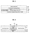
- FIGs. 3 to 5 are diagrams showing a nitride semiconductor laser diode having a ridge structure on an n-type layer for explaining a method for manufacturing the same in accordance with a preferred embodiment of the present invention.
- FIG. 6 is a cross-sectional view illustrating a nitride semiconductor laser diode having a ridge structure formed on an n-type layer in accordance with a preferred embodiment of the present invention.
- FIGs 3 to 5 are diagrams for explaining a method for manufacturing a nitride semiconductor laser diode having a ridge structure on an n-type layer by using a wafer bonding technique in accordance with a preferred embodiment of the present invention.
- a nitride epilayer 102 shown in Fig. 1 is formed on substrate 101 made of a sapphire (Al203), SiC or a GaN l at first.
- a GaN layer (undoped GaN), an n-GaN layer, a compliance layer (InGaN), an n-cladding layer (n-ALGaN)), an n-waveguide (GaN) layer, a multi-quantum well (MQW), an electron blocking layer (EBL), a p-waveguide (GaN) layer a p-cladding layer (P-AlGaN) and a capping layer (P-GaN) are orderly formed on the substrates 101.
- a p-ohmic metal layer 103 is evaporated on the nitride epilayer 102.
- a metal is generally used as the p-Ohmic metal layer 103.
- the p-ohmic metal layer 103 may be formed by using a conductive material adjustable to a wavefunction of the p-layer.
- a pad metal and a bending metal 104 are evaporated on the p-ohmic metal layer 103.
- a thermal treatment is performed for making an ohmic state between the capping layer (P-GaN) and the P-Ohmic metal 103.
- the thermal treatment may be not performed after evaporating the pad metal and the bending metal 104.
- the ohmic state may be made by a later thermal treatment for bonding fixing substrate 106 and a nitride structure.
- the bonding metal 105 is evaporated on a fixing substrate 106.
- the fixing substrate 106 is used for fixing the evaporated structure shown in Fig. 3 and a GaAs or a Si is generally used for the fixing substrate 106.
- the bonding metal 105 evaporated fixing substrate 106 is coupled to the nitride structure of Fig. 3 by compressed and thermal processed as shown in Fig. 5.
- the ohmic state between the capping layer (P-GaN) and the p-ohmic metal 103 may be made by the thermal process.
- an n-type layer may be exposed by lapping an undoped GaN layer in the nitride epilayer 102 and the substrate layer 101.
- a Reactive Ion Etching process and a thermal process are performed.
- the RIE and thermal process are performed for preventing an ohmic contact between an n-pad metal and n-type layer. That is, it prevents increase of contact resistivity.
- predetermined portions of a left side and a right side of the exposed n-type layer are eliminated by etching the predetermined portions of the left and the right sides of the exposed n-type layer. That is, a center part of the exposed n-type layer is left.
- the exposed n-type layer is etched for projecting a center part of the n-type layer including the n-GaN layer, the InGaN layer and the n-cladding layer. That is, a ridge structure is formed at center part of the n-type layer.
- an insulating layer is evaporated on the right and the left sides of the exposed n-type.
- an n-pad metal is evaporated on the insulating layer and the ridge structure.
- Fig. 6 shows a nitride semiconductor layer diode including a ridge structure on an n-type layer manufactured by the above mentioned method.
- an n-cladding layer 110 having a ridge structure is formed on a center of an n-waveguide (GaN) layer 112.
- the n-waveguide layer 112 is formed on a multi-quantum well (MQW) 113 and an electron blocking layer (EBL) 114.
- MQW multi-quantum well
- EBL electron blocking layer
- an InGaN layer 109, an n-GaN layer 108 are orderly evaporated to form the ridge structure.
- an insulating layer 111 is formed at the sides of the ridge structure and on the n-waveguide layer 112.
- An n-pad metal layer 107 is formed on the insulating layer 111 and the n-GaN layer 108.
- the ridge structure is formed on the n-type layer in the present invention, where the n-type layer has a superior carrier concentration characteristics and a superior mobility comparing to a p-type layer. Therefore, a resistance becomes decreased (the carrier concentration and the mobility is reverse proportional to the resistance) and it becomes easy to form the ohmic contact metal layer 108.
- processes are formed to manufacture a laser diode package by using a junction-up/down or top-down method.
- the present invention provides a method easily forming the ridge structure on the n-type layer by fixing the nitride semiconductor layer by using the fixing substrate.
- the present invention increases I-V characteristics of elements, suppresses heat generation and extends the lifetime by forming the ridge structure on the n-type layer.
Landscapes
- Engineering & Computer Science (AREA)
- Physics & Mathematics (AREA)
- Nanotechnology (AREA)
- Chemical & Material Sciences (AREA)
- Optics & Photonics (AREA)
- Electromagnetism (AREA)
- General Physics & Mathematics (AREA)
- Condensed Matter Physics & Semiconductors (AREA)
- Life Sciences & Earth Sciences (AREA)
- Biophysics (AREA)
- Crystallography & Structural Chemistry (AREA)
- Power Engineering (AREA)
- Manufacturing & Machinery (AREA)
- Semiconductor Lasers (AREA)
Abstract
Description
- This application claims the benefit of the Korean Application No. 10-2004-0003891 filed on January 19, 2004, which is hereby incorporated by reference.
- The present invention relates to a nitride semiconductor laser diode, and more particularly, to a method for manufacturing a nitride semiconductor laser diode having a ridge structure on an n-type layer.
- Generally, a nitride semiconductor laser diode has been developed and manufactured to be applied to a mass information storage device and a color printer. Also, there have been various applications introduced by using the nitride semiconductor laser diode.
- For applying the nitride semiconductor laser diode to the mass information storage device and the color printer, the nitride semiconductor laser diode is required to have characteristics including low threshold current (Ith), high external quantum efficiency (ηex) and low operating voltage (Vop) for providing high reliability related to a lifetime and low power consumption.
- The low operating voltage is a major factor to be improved in the nitride semiconductor laser diode. That is, a current-voltage characteristic (I-V) of the nitride semiconductor laser diode must be improved.
- A conventional nitride semiconductor laser diode will be described below with reference to FIG. 1.
- FIG. 1 is a cross-sectional view of a conventional nitride semiconductor laser diode. As shown in FIG. 1, the conventional nitride semiconductor laser diode includes an
undoped GaN layer 1 formed on a substrate (not shown) made of a GaN or a sapphire, an n-GaN layer 2, a compliance layer (InGaN) 3, an n-cladding layer (n-ALGaN) 4, an n-waveguide (GaN)layer 5, a multi-quantum well (MQW) 6, an electron blocking layer (EBL) 7, a p-waveguide layer (GaN) 8, a p-cladding layer (p-AlGaN) 9, a capping layer (p-GaN) 10, and a p-pad metal layer (not shown) formed on thecapping layer 10. - In FIG. 1, the n-
GaN layer 2 is extended to a right and a left directions with a substrate (not shown) and an exposed n-pad metal layer (not shown) is formed by mesa etching the expended the n-GaN layer 2 and the substrate (not shown). - The conventional nitride semiconductor laser diode is a p-n diode form. That is, the conventional nitride semiconductor laser diode includes the
multi-quantum well MQW 6 emitting lights, and GaNwaveguide layers cladding layers - The nitride semiconductor laser diode receives current from the p-pad metal layer (not shown) and emits the lights by coupling an electron and a hole at the
MQW 6. The light is externally radiated through the capping layer (p-GaN) 10. - When emitting the light, the
GaN waveguide layers AlGaN Cladding layers MQW 6 and guide the emitted lights. - For effectively emitting a laser beam and improving beam characteristics of a laser diode, a ridge structure has been implemented to a nitride semiconductor laser diode.
- FIG. 2 is a cross-sectional view of a conventional nitride semiconductor laser diode having a ridge structure.
- As shown in FIG. 2, the nitride semiconductor laser diode having the ridge structure includes: a p-
cladding layer 9 formed on anMQW 6, aEBL 7 and a P-waveguide layer 8, where a center part of the p-cladding layer 9 is projected and theMQW 6, theEBL 7 and the P-waveguide layer 8 are identical to the same of FIG. 1; acapping layer 10 formed on an upper surface of the projected part of p-cladding layer 9; and anohmic contact metal 11 formed on thecapping layer 10. In FIG. 2, the projected part of the p-cladding layer 9, thecapping layer 10 and the ohmiccontact metal layer 11 are formed the ridge structure. - The ridge structure is generally manufactured to have a width less than 3 µm and a current from the p-
pad metal layer 13 is flowed through the ridge structure. - An
insulating layer 12 is formed at side surfaces of the ridge structure and on an upper surface of the p-waveguide layer 8. After forming theinsulating layer 12, a p-pad metal layer 13 is formed on the insulatinglayer 12 and the ohmiccontact metal layer 11. - According to the above-mentioned related art, the ridge structure is generally formed on the p-
type layers - When the p-type layer is growth, a magnesium Mg is used as a dopant. The p-type layer must be formed after forming the n-type layer, the waveguide layer and the MQW because the Mg has a memory effect. Accordingly, it is structurally simple and convenience to form the ridge structure on the p-type layer.
- However, the nitride has a large band gap, a low carrier concentration and a low mobility. Therefore, it is difficult to form the ohmic
contact metal layer 11 comparing to other compound semiconductor. - Also, a resistance seriously increases since the p-type layer has low carrier concentration and low mobility comparing to the n-type layer and it is difficult to form the
ohmic contact metal 11. - Furthermore, the ridge structure according to the related art causes sudden increase of element resistance. It degrades I-V characteristics of the nitride semiconductor laser diode.
- The increase of resistance induces to increase an operating voltage and causes to generate heat from a part of the ridge contacted to the p-pad metal. Therefore, the p-ohmic metal and element characteristics are degraded and the reliability of the laser diode such as the lift time decreases.
- Accordingly, the present invention is directed to a a nitride semiconductor laser diode having a ridge structure on an n-type layer and a method for manufacturing the same that substantially obviates one or more problems due to limitations and disadvantages of the related art.
- An object of the present invention is to provide a method for manufacturing a nitride semiconductor laser diode having a ridge structure formed on an n-type layer instead of forming the ridge structure on a p-type layer having comparatively large resistance and a difficulty to form an ohmic contact layer.
- Additional advantages, objects, and features of the invention will be set forth in part in the description which follows and in part will become apparent to those having ordinary skill in the art upon examination of the following or may be learned from practice of the invention. The objectives and other advantages of the invention may be realized and attained by the structure particularly pointed out in the written description and claims hereof as well as the appended drawings.
- To achieve these objects and other advantages and in accordance with the purpose of the invention, as embodied and broadly described herein, there is provided a method for manufacturing a nitride semiconductor laser diode, the method including the steps of: a) forming a nitride semiconductor layer by orderly evaporating a substrate, an undoped GaN layer, an n-type layer, a multi-quantum well (MQW), an electron blocking layer (EBL) and a p-type layer; b) eliminating the substrate and the undoped GaN layer in the nitride semiconductor layer by lapping the substrate and the undoped GaN layer; and c) forming a ridge structure on the n-type layer.
- The method may further include the step of d) fixing the nitride semiconductor layer by using a fixing substrate, wherein the fixing substrate is bonded on an upper side of the p-type layer.
- The step of fixing the nitride semiconductor layer may include the steps of: d-1) evaporating a p-ohmic metal on an upper side of the p-type layer; d-2) evaporating a pad-metal and a bonding metal on an upper side of the p-ohmic metal; d-3) bonding the bonding metal to the fixing substrate; and d-4) fixing the bonding metal evaporated fixing substrate to the pad metal and the bonding metal by compressing and thermal processing.
- The step of fixing the nitride semiconductor layer may further include the step of d-5) performing a thermal process for making an ohmic state between the p-GaN layer on the p-type layer and the p-ohmic metal layer.
- The step of forming the ridge structure may include the steps of: c-1) eliminating predetermined portions of a right and a left sides of the n-type layer by etching the right and the left sides of the n-type layer for remaining a center portion of the n-type layer; and c-2) evaporating an insulating layer on the eliminated sides of the n-type layer.
- In another aspect of the present invention, there is provided a nitride semiconductor laser diode including an n-type layer, an activate layer, an EBL and a p-type layer, wherein the n-type layer has a ridge structure.
- Accordingly, the present invention provides a method for easily forming a ridge structure on an n-type layer, improving I-V characteristics, suppressing heat generation and extending an operational lifetime.
- It is to be understood that both the foregoing general description and the following detailed description of the present invention are exemplary and explanatory and are intended to provide further explanation of the invention as claimed.
- The accompanying drawings, which are included to provide a further understanding of the invention and are incorporated in and constitute a part of this application, illustrate embodiment(s) of the invention and together with the description serve to explain the principle of the invention. In the drawings:
- FIG. 1 is a diagram of a conventional nitride semiconductor laser diode;
- FIG. 2 is a diagram of a conventional nitride semiconductor laser diode having a ridge structure;
- FIGs. 3 to 5 are diagrams showing a nitride semiconductor laser diode having a ridge structure on an n-type layer for explaining a method for manufacturing the same in accordance with a preferred embodiment of the present invention; and
- FIG. 6 is a cross-sectional view illustrating a nitride semiconductor laser diode having a ridge structure formed on an n-type layer in accordance with a preferred embodiment of the present invention.
- Reference will now be made in detail to the preferred embodiments of the present invention, examples of which are illustrated in the accompanying drawings. Wherever possible, the same reference numbers will be used throughout the drawings to refer to the same or like parts.
- FIGs 3 to 5 are diagrams for explaining a method for manufacturing a nitride semiconductor laser diode having a ridge structure on an n-type layer by using a wafer bonding technique in accordance with a preferred embodiment of the present invention.
- As shown in FIG. 3, a
nitride epilayer 102 shown in Fig. 1 is formed onsubstrate 101 made of a sapphire (Al203), SiC or a GaN l at first. - That is, a GaN layer (undoped GaN), an n-GaN layer, a compliance layer (InGaN), an n-cladding layer (n-ALGaN)), an n-waveguide (GaN) layer, a multi-quantum well (MQW), an electron blocking layer (EBL), a p-waveguide (GaN) layer a p-cladding layer (P-AlGaN) and a capping layer (P-GaN) are orderly formed on the
substrates 101. - After forming the capping layer (P-GaN), a p-
ohmic metal layer 103 is evaporated on thenitride epilayer 102. A metal is generally used as the p-Ohmic metal layer 103. However, the p-ohmic metal layer 103 may be formed by using a conductive material adjustable to a wavefunction of the p-layer. - After evaporating the p-
ohmic metal layer 103, a pad metal and a bendingmetal 104 are evaporated on the p-ohmic metal layer 103. - When the evaporating, a thermal treatment is performed for making an ohmic state between the capping layer (P-GaN) and the P-
Ohmic metal 103. However, the thermal treatment may be not performed after evaporating the pad metal and the bendingmetal 104. The ohmic state may be made by a later thermal treatment forbonding fixing substrate 106 and a nitride structure. - After performing the thermal treatment, the
bonding metal 105 is evaporated on a fixingsubstrate 106. The fixingsubstrate 106 is used for fixing the evaporated structure shown in Fig. 3 and a GaAs or a Si is generally used for the fixingsubstrate 106. - The
bonding metal 105 evaporated fixingsubstrate 106 is coupled to the nitride structure of Fig. 3 by compressed and thermal processed as shown in Fig. 5. - During the coupling, the ohmic state between the capping layer (P-GaN) and the p-
ohmic metal 103 may be made by the thermal process. - As shown in Fig. 5, an n-type layer may be exposed by lapping an undoped GaN layer in the
nitride epilayer 102 and thesubstrate layer 101. - For reducing damages on the n-type layer caused by lapping, a Reactive Ion Etching process and a thermal process are performed. The RIE and thermal process are performed for preventing an ohmic contact between an n-pad metal and n-type layer. That is, it prevents increase of contact resistivity.
- After eliminating undoped GaN layer, predetermined portions of a left side and a right side of the exposed n-type layer are eliminated by etching the predetermined portions of the left and the right sides of the exposed n-type layer. That is, a center part of the exposed n-type layer is left.
- In other words, the exposed n-type layer is etched for projecting a center part of the n-type layer including the n-GaN layer, the InGaN layer and the n-cladding layer. That is, a ridge structure is formed at center part of the n-type layer.
- After etching, an insulating layer is evaporated on the right and the left sides of the exposed n-type. After forming the insulating layer, an n-pad metal is evaporated on the insulating layer and the ridge structure.
- Fig. 6 shows a nitride semiconductor layer diode including a ridge structure on an n-type layer manufactured by the above mentioned method.
- As shown in Fig. 6, an n-
cladding layer 110 having a ridge structure is formed on a center of an n-waveguide (GaN)layer 112. The n-waveguide layer 112 is formed on a multi-quantum well (MQW) 113 and an electron blocking layer (EBL) 114. On the n-cladding layer 110, anInGaN layer 109, an n-GaN layer 108 are orderly evaporated to form the ridge structure. - And, an insulating
layer 111 is formed at the sides of the ridge structure and on the n-waveguide layer 112. An n-pad metal layer 107 is formed on the insulatinglayer 111 and the n-GaN layer 108. - As mentioned above, the ridge structure is formed on the n-type layer in the present invention, where the n-type layer has a superior carrier concentration characteristics and a superior mobility comparing to a p-type layer. Therefore, a resistance becomes decreased (the carrier concentration and the mobility is reverse proportional to the resistance) and it becomes easy to form the ohmic
contact metal layer 108. - After forming the ridge structure as mentioned above, processes are formed to manufacture a laser diode package by using a junction-up/down or top-down method.
- As mentioned above, the present invention provides a method easily forming the ridge structure on the n-type layer by fixing the nitride semiconductor layer by using the fixing substrate.
- Also, the present invention increases I-V characteristics of elements, suppresses heat generation and extends the lifetime by forming the ridge structure on the n-type layer.
- It will be apparent to those skilled in the art that various modifications and variations can be made in the present invention. Thus, it is intended that the present invention covers the modifications and variations of this invention provided they come within the scope of the appended claims and their equivalents.
- The claims refer to examples of preferred embodiments of the invention. However, the invention also refers to the use of any single feature and subcombination of features which are disclosed in the claims, the description and / or the drawings.
Claims (18)
- A method for manufacturing a nitride semiconductor laser diode, the method comprising the steps of:a) forming a nitride semiconductor layer by orderly evaporating a substrate, an undoped GaN layer, an n-type layer, a multi-quantum well (MQW), an electron blocking layer (EBL) and a p-type layer;b) eliminating the substrate and the undoped GaN layer in the nitride semiconductor layer by lapping the substrate and the undoped GaN layer; andc) forming a ridge structure on the n-type layer.
- The method of claim 1, further comprising the step of d) fixing the nitride semiconductor layer by using a fixing substrate.
- The method of claim 2, wherein the fixing substrate is bonded on an upper side of the p-type layer.
- The method of claim 2, wherein the nitride semiconductor layer is fixed by the fixing substrate before eliminating the substrate and the undoped GaN layer.
- The method of claim 2, wherein the fixing substrate is made of a GaAs or a Si having high thermal conductivity.
- The method of claim 2, wherein the step d) includes the steps of:d-1) evaporating a p-ohmic metal on an upper side of the p-type layer;d-2) evaporating a pad-metal and a bonding metal on an upper side of the p-ohmic metal;d-3) bonding the bonding metal to the fixing substrate; andd-4) fixing the bonding metal evaporated fixing substrate to the pad metal and the bonding metal by compressing and thermal processing.
- The method of claim 6, wherein the step d) further includes the step of d-5) performing a thermal process for making an ohmic state between the p-GaN layer on the p-type layer and the p-ohmic metal layer.
- The method of claim 1, the method further comprising the step e) performing a reactive ion etching (RIE) process and a thermal process for reducing loss of the eliminated side.
- The method of claim 1, the step c) includes the steps of:c-1) eliminating predetermined portions of a right and a left sides of the n-type layer by etching the right and the left sides of the n-type layer for remaining a center portion of the n-type layer; andc-2) evaporating an insulating layer on the eliminated sides of the n-type layer.
- The method of claim 9, wherein the left and the right sides eliminated n-type layer is an n-cladding layer, an InGaN layer and n-GaN layer.
- The method of claim 1, further comprising the step f) forming an n-pad metal on an upper side of the ridge structure.
- A method for manufacturing a nitride semiconductor laser diode, the method comprising the steps of:a) forming a nitride semiconductor layer by orderly evaporating a substrate, an undoped GaN layer, an n-type layer, a multi-quantum well (MQW), an electron blocking layer (EBL) and a p-type layer;b) fixing the nitride semiconductor layer by bonding to a fixing substrate on an upper side of the p-type layer;c) eliminating the substrate and the undoped GaN layer of the nitride semiconductor layer;d) forming a ridge structure on the n-type layer; ande) forming an n-pad metal on an upper side of the ridge structure.
- A method for manufacturing a nitride semiconductor laser diode, the method comprising:a) forming a nitride semiconductor layer;b) fixing the nitride semiconductor layer by using a fixing substrate;c) eliminating a bottom of an n-type layer of the nitride semiconductor layer by lapping the bottom of the n-type layer; andd) forming a ridge structure on the n-type layer.
- The method of claim 13, wherein the eliminated bottom of the n-type layer is a substrate or an undoped GaN layer.
- The method of claim 13, wherein the step d) includes the steps of:d-1) eliminating predetermined portions of a right side and a left side of the n-type layer for remaining a center part of the n-type layer left by etching the predetermined portions of the right and the left sides of the n-type layer; andd-2) evaporating an insulating layer on the eliminated right and left sides of the n-type layer.
- A nitride semiconductor laser diode comprising an n-type layer, an activate layer, an EBL and a p-type layer, wherein the n-type layer has a ridge structure.
- The nitride semiconductor laser diode of claim 16, wherein the n-type layer includes an n-GaN layer, an n-waveguide layer, an n-cladding layer, an n-GaN layer, an n-pad metal layer where they are orderly evaporated and the n-cladding layer, the In GaN layer and the n-GaN layer form the ridge structure.
- The nitride semiconductor laser diode of claim 16, wherein an insulating layer is formed on a left side and a right side of the n-type layer having the ridge structure.
Applications Claiming Priority (2)
| Application Number | Priority Date | Filing Date | Title |
|---|---|---|---|
| KR1020040003891A KR101014720B1 (en) | 2004-01-19 | 2004-01-19 | Semiconductor laser diode manufacturing method |
| KR2004003891 | 2004-01-19 |
Publications (3)
| Publication Number | Publication Date |
|---|---|
| EP1555732A2 true EP1555732A2 (en) | 2005-07-20 |
| EP1555732A3 EP1555732A3 (en) | 2007-07-25 |
| EP1555732B1 EP1555732B1 (en) | 2016-03-30 |
Family
ID=34617471
Family Applications (1)
| Application Number | Title | Priority Date | Filing Date |
|---|---|---|---|
| EP05000651.9A Ceased EP1555732B1 (en) | 2004-01-19 | 2005-01-14 | Method for manufacturing a nitride semiconductor laser diode |
Country Status (5)
| Country | Link |
|---|---|
| US (1) | US7074633B2 (en) |
| EP (1) | EP1555732B1 (en) |
| JP (1) | JP2005210124A (en) |
| KR (1) | KR101014720B1 (en) |
| CN (1) | CN1328832C (en) |
Families Citing this family (2)
| Publication number | Priority date | Publication date | Assignee | Title |
|---|---|---|---|---|
| JP4984178B2 (en) | 2006-12-25 | 2012-07-25 | 国立大学法人九州工業大学 | High frequency signal interpolation apparatus and high frequency signal interpolation method |
| CN116470388A (en) * | 2023-05-30 | 2023-07-21 | 厦门市三安光电科技有限公司 | Laser chips and lasers |
Citations (4)
| Publication number | Priority date | Publication date | Assignee | Title |
|---|---|---|---|---|
| JPH1027940A (en) | 1996-07-12 | 1998-01-27 | Matsushita Electric Ind Co Ltd | Semiconductor laser device |
| GB2346478A (en) | 1999-02-05 | 2000-08-09 | Agilent Technologies Inc | Optical emission device |
| US6455340B1 (en) | 2001-12-21 | 2002-09-24 | Xerox Corporation | Method of fabricating GaN semiconductor structures using laser-assisted epitaxial liftoff |
| US20030052316A1 (en) | 2001-09-07 | 2003-03-20 | Nec Corporation | Gallium nitride based compound semiconductor light-emitting device |
Family Cites Families (11)
| Publication number | Priority date | Publication date | Assignee | Title |
|---|---|---|---|---|
| JP4118025B2 (en) * | 1996-02-21 | 2008-07-16 | シャープ株式会社 | Gallium nitride semiconductor laser device |
| JP3467981B2 (en) * | 1996-07-19 | 2003-11-17 | ソニー株式会社 | Method of forming light emitting end face of semiconductor light emitting element, method of manufacturing semiconductor light emitting element, semiconductor light emitting element, method of forming end face of nitride III-V compound semiconductor layer, method of manufacturing semiconductor device, and semiconductor device |
| JP3087829B2 (en) * | 1996-10-14 | 2000-09-11 | 日亜化学工業株式会社 | Method for manufacturing nitride semiconductor device |
| US6744800B1 (en) * | 1998-12-30 | 2004-06-01 | Xerox Corporation | Method and structure for nitride based laser diode arrays on an insulating substrate |
| TW502458B (en) * | 1999-06-09 | 2002-09-11 | Toshiba Corp | Bonding type semiconductor substrate, semiconductor light emission element and manufacturing method thereof |
| KR100397609B1 (en) * | 2001-02-16 | 2003-09-13 | 삼성전기주식회사 | Semiconductor laser diode capable of controlling width of carrier inflow path |
| JP2002335048A (en) * | 2001-03-06 | 2002-11-22 | Sony Corp | Nitride-based semiconductor laser device and method of manufacturing the same |
| TW521448B (en) * | 2001-03-09 | 2003-02-21 | Seiko Epson Corp | Method of fabricating surface-emission type light-emitting device, surface-emitting semiconductor laser, method of fabricating the same, optical module and optical transmission device |
| JP4066681B2 (en) * | 2001-03-21 | 2008-03-26 | 日亜化学工業株式会社 | Light emitting device and method for manufacturing light emitting device |
| KR20030040671A (en) * | 2001-11-15 | 2003-05-23 | 주식회사 엘지이아이 | Method for fabricating Laser diode |
| JP2003234535A (en) * | 2003-03-10 | 2003-08-22 | Sony Corp | Method of forming light emitting end face of semiconductor light emitting element, method of manufacturing semiconductor light emitting element, semiconductor light emitting element, method of manufacturing semiconductor device, and semiconductor device |
-
2004
- 2004-01-19 KR KR1020040003891A patent/KR101014720B1/en not_active Expired - Fee Related
-
2005
- 2005-01-14 EP EP05000651.9A patent/EP1555732B1/en not_active Ceased
- 2005-01-18 US US11/036,377 patent/US7074633B2/en not_active Expired - Fee Related
- 2005-01-18 CN CNB2005100018542A patent/CN1328832C/en not_active Expired - Fee Related
- 2005-01-19 JP JP2005011701A patent/JP2005210124A/en active Pending
Patent Citations (4)
| Publication number | Priority date | Publication date | Assignee | Title |
|---|---|---|---|---|
| JPH1027940A (en) | 1996-07-12 | 1998-01-27 | Matsushita Electric Ind Co Ltd | Semiconductor laser device |
| GB2346478A (en) | 1999-02-05 | 2000-08-09 | Agilent Technologies Inc | Optical emission device |
| US20030052316A1 (en) | 2001-09-07 | 2003-03-20 | Nec Corporation | Gallium nitride based compound semiconductor light-emitting device |
| US6455340B1 (en) | 2001-12-21 | 2002-09-24 | Xerox Corporation | Method of fabricating GaN semiconductor structures using laser-assisted epitaxial liftoff |
Non-Patent Citations (1)
| Title |
|---|
| JOURNAL OF CRYSTAL GROWTH, vol. 226, no. 1, pages 73 - 78 |
Also Published As
| Publication number | Publication date |
|---|---|
| CN1645693A (en) | 2005-07-27 |
| EP1555732A3 (en) | 2007-07-25 |
| KR101014720B1 (en) | 2011-02-16 |
| US20050157768A1 (en) | 2005-07-21 |
| US7074633B2 (en) | 2006-07-11 |
| EP1555732B1 (en) | 2016-03-30 |
| JP2005210124A (en) | 2005-08-04 |
| KR20050076089A (en) | 2005-07-26 |
| CN1328832C (en) | 2007-07-25 |
Similar Documents
| Publication | Publication Date | Title |
|---|---|---|
| JP4904261B2 (en) | Light emitting device having current blocking structure and method for manufacturing light emitting device having current blocking structure | |
| EP1411559B1 (en) | Semiconductor optoelectronic device | |
| US7705363B2 (en) | Light emitting device having a light extraction structure | |
| US6185238B1 (en) | Nitride compound semiconductor laser and its manufacturing method | |
| CN112868109B (en) | Semiconductor light emitting device | |
| CN113851932B (en) | Semiconductor laser diode | |
| US20110227033A1 (en) | Semiconductor light emitting device, wafer, method for manufacturing semiconductor light emitting device, and method for manufacturing wafer | |
| US20090026487A1 (en) | Light-emitting devices having an active region with electrical contacts coupled to opposing surfaces thereof and methods of forming the same | |
| US9214595B2 (en) | Semiconductor light emitting device | |
| US20130015465A1 (en) | Nitride semiconductor light-emitting device | |
| US7095041B2 (en) | High-efficiency light emitting diode | |
| JP2800666B2 (en) | Gallium nitride based compound semiconductor laser device | |
| CN101878546A (en) | Optoelectronic semiconductor body and method for producing an optoelectronic semiconductor body | |
| JP2000232259A (en) | Light emitting device and manufacturing method thereof | |
| US7074633B2 (en) | Nitride semiconductor laser diode and method for manufacturing the same | |
| JPH10294533A (en) | Nitride compound semiconductor laser and method of manufacturing the same | |
| US20060180819A1 (en) | Reflective electrode and compound semiconductor light emitting device including the same | |
| KR100991784B1 (en) | How to reduce wafer bending of nitride semiconductor laser diodes | |
| KR100599055B1 (en) | Semiconductor light emitting device | |
| US7288793B2 (en) | Semiconductor laser | |
| US20250192521A1 (en) | Light-emitting diode | |
| KR20060092588A (en) | Manufacturing method of laser diode | |
| JP2006332600A (en) | Nitride-based semiconductor laser diode and manufacturing method thereof | |
| KR20180118898A (en) | Semiconductor laser light emitting device | |
| JP2007188928A (en) | Nitride semiconductor light emitting device |
Legal Events
| Date | Code | Title | Description |
|---|---|---|---|
| PUAI | Public reference made under article 153(3) epc to a published international application that has entered the european phase |
Free format text: ORIGINAL CODE: 0009012 |
|
| 17P | Request for examination filed |
Effective date: 20050122 |
|
| AK | Designated contracting states |
Kind code of ref document: A2 Designated state(s): AT BE BG CH CY CZ DE DK EE ES FI FR GB GR HU IE IS IT LI LT LU MC NL PL PT RO SE SI SK TR |
|
| AX | Request for extension of the european patent |
Extension state: AL BA HR LV MK YU |
|
| PUAL | Search report despatched |
Free format text: ORIGINAL CODE: 0009013 |
|
| AK | Designated contracting states |
Kind code of ref document: A3 Designated state(s): AT BE BG CH CY CZ DE DK EE ES FI FR GB GR HU IE IS IT LI LT LU MC NL PL PT RO SE SI SK TR |
|
| AX | Request for extension of the european patent |
Extension state: AL BA HR LV MK YU |
|
| AKX | Designation fees paid |
Designated state(s): DE FR GB NL |
|
| 17Q | First examination report despatched |
Effective date: 20110124 |
|
| GRAP | Despatch of communication of intention to grant a patent |
Free format text: ORIGINAL CODE: EPIDOSNIGR1 |
|
| INTG | Intention to grant announced |
Effective date: 20150929 |
|
| GRAS | Grant fee paid |
Free format text: ORIGINAL CODE: EPIDOSNIGR3 |
|
| GRAA | (expected) grant |
Free format text: ORIGINAL CODE: 0009210 |
|
| AK | Designated contracting states |
Kind code of ref document: B1 Designated state(s): DE FR GB NL |
|
| REG | Reference to a national code |
Ref country code: GB Ref legal event code: FG4D |
|
| REG | Reference to a national code |
Ref country code: DE Ref legal event code: R096 Ref document number: 602005048787 Country of ref document: DE |
|
| REG | Reference to a national code |
Ref country code: NL Ref legal event code: FP |
|
| REG | Reference to a national code |
Ref country code: FR Ref legal event code: PLFP Year of fee payment: 13 |
|
| REG | Reference to a national code |
Ref country code: DE Ref legal event code: R097 Ref document number: 602005048787 Country of ref document: DE |
|
| PLBE | No opposition filed within time limit |
Free format text: ORIGINAL CODE: 0009261 |
|
| STAA | Information on the status of an ep patent application or granted ep patent |
Free format text: STATUS: NO OPPOSITION FILED WITHIN TIME LIMIT |
|
| 26N | No opposition filed |
Effective date: 20170103 |
|
| REG | Reference to a national code |
Ref country code: FR Ref legal event code: PLFP Year of fee payment: 14 |
|
| PGFP | Annual fee paid to national office [announced via postgrant information from national office to epo] |
Ref country code: NL Payment date: 20191206 Year of fee payment: 16 |
|
| PGFP | Annual fee paid to national office [announced via postgrant information from national office to epo] |
Ref country code: FR Payment date: 20191209 Year of fee payment: 16 |
|
| PGFP | Annual fee paid to national office [announced via postgrant information from national office to epo] |
Ref country code: DE Payment date: 20191205 Year of fee payment: 16 Ref country code: GB Payment date: 20191209 Year of fee payment: 16 |
|
| REG | Reference to a national code |
Ref country code: DE Ref legal event code: R119 Ref document number: 602005048787 Country of ref document: DE |
|
| REG | Reference to a national code |
Ref country code: NL Ref legal event code: MM Effective date: 20210201 |
|
| GBPC | Gb: european patent ceased through non-payment of renewal fee |
Effective date: 20210114 |
|
| PG25 | Lapsed in a contracting state [announced via postgrant information from national office to epo] |
Ref country code: NL Free format text: LAPSE BECAUSE OF NON-PAYMENT OF DUE FEES Effective date: 20210201 Ref country code: FR Free format text: LAPSE BECAUSE OF NON-PAYMENT OF DUE FEES Effective date: 20210131 |
|
| PG25 | Lapsed in a contracting state [announced via postgrant information from national office to epo] |
Ref country code: GB Free format text: LAPSE BECAUSE OF NON-PAYMENT OF DUE FEES Effective date: 20210114 Ref country code: DE Free format text: LAPSE BECAUSE OF NON-PAYMENT OF DUE FEES Effective date: 20210803 |