EP1554780B1 - Sub-millimeter wavelength camera - Google Patents
Sub-millimeter wavelength camera Download PDFInfo
- Publication number
- EP1554780B1 EP1554780B1 EP03778333A EP03778333A EP1554780B1 EP 1554780 B1 EP1554780 B1 EP 1554780B1 EP 03778333 A EP03778333 A EP 03778333A EP 03778333 A EP03778333 A EP 03778333A EP 1554780 B1 EP1554780 B1 EP 1554780B1
- Authority
- EP
- European Patent Office
- Prior art keywords
- mask
- antenna
- mixer
- radiation
- millimeter
- Prior art date
- Legal status (The legal status is an assumption and is not a legal conclusion. Google has not performed a legal analysis and makes no representation as to the accuracy of the status listed.)
- Expired - Lifetime
Links
- 238000003384 imaging method Methods 0.000 claims abstract description 29
- 230000005855 radiation Effects 0.000 claims abstract description 28
- 239000000758 substrate Substances 0.000 claims abstract description 25
- 238000000059 patterning Methods 0.000 claims abstract description 8
- 238000004891 communication Methods 0.000 claims abstract description 6
- 230000005670 electromagnetic radiation Effects 0.000 claims abstract description 5
- 238000000034 method Methods 0.000 claims description 13
- 230000001154 acute effect Effects 0.000 claims description 5
- VYPSYNLAJGMNEJ-UHFFFAOYSA-N Silicium dioxide Chemical compound O=[Si]=O VYPSYNLAJGMNEJ-UHFFFAOYSA-N 0.000 claims description 4
- 229910052751 metal Inorganic materials 0.000 claims description 3
- 239000002184 metal Substances 0.000 claims description 3
- 229920002120 photoresistant polymer Polymers 0.000 claims description 3
- 229910017083 AlN Inorganic materials 0.000 claims description 2
- PIGFYZPCRLYGLF-UHFFFAOYSA-N Aluminum nitride Chemical compound [Al]#N PIGFYZPCRLYGLF-UHFFFAOYSA-N 0.000 claims description 2
- 239000000377 silicon dioxide Substances 0.000 claims description 2
- 235000012239 silicon dioxide Nutrition 0.000 claims description 2
- 230000000295 complement effect Effects 0.000 claims 1
- XUIMIQQOPSSXEZ-UHFFFAOYSA-N Silicon Chemical group [Si] XUIMIQQOPSSXEZ-UHFFFAOYSA-N 0.000 description 18
- 229910052710 silicon Inorganic materials 0.000 description 16
- 239000010703 silicon Substances 0.000 description 16
- 238000005530 etching Methods 0.000 description 7
- 238000001514 detection method Methods 0.000 description 5
- 238000004519 manufacturing process Methods 0.000 description 5
- 239000000463 material Substances 0.000 description 4
- 230000003287 optical effect Effects 0.000 description 2
- 239000004065 semiconductor Substances 0.000 description 2
- 238000001228 spectrum Methods 0.000 description 2
- 239000000126 substance Substances 0.000 description 2
- 230000007704 transition Effects 0.000 description 2
- 208000000453 Skin Neoplasms Diseases 0.000 description 1
- 150000001408 amides Chemical class 0.000 description 1
- 150000001412 amines Chemical class 0.000 description 1
- 239000000470 constituent Substances 0.000 description 1
- 238000010586 diagram Methods 0.000 description 1
- 239000006185 dispersion Substances 0.000 description 1
- 230000000694 effects Effects 0.000 description 1
- 238000005516 engineering process Methods 0.000 description 1
- 238000005259 measurement Methods 0.000 description 1
- 239000000203 mixture Substances 0.000 description 1
- 230000000135 prohibitive effect Effects 0.000 description 1
- 238000002310 reflectometry Methods 0.000 description 1
- 230000003068 static effect Effects 0.000 description 1
- 238000011144 upstream manufacturing Methods 0.000 description 1
Images




Classifications
-
- H—ELECTRICITY
- H01—ELECTRIC ELEMENTS
- H01Q—ANTENNAS, i.e. RADIO AERIALS
- H01Q21/00—Antenna arrays or systems
- H01Q21/06—Arrays of individually energised antenna units similarly polarised and spaced apart
- H01Q21/061—Two dimensional planar arrays
- H01Q21/064—Two dimensional planar arrays using horn or slot aerials
-
- H—ELECTRICITY
- H01—ELECTRIC ELEMENTS
- H01Q—ANTENNAS, i.e. RADIO AERIALS
- H01Q13/00—Waveguide horns or mouths; Slot antennas; Leaky-waveguide antennas; Equivalent structures causing radiation along the transmission path of a guided wave
- H01Q13/02—Waveguide horns
-
- H—ELECTRICITY
- H01—ELECTRIC ELEMENTS
- H01Q—ANTENNAS, i.e. RADIO AERIALS
- H01Q13/00—Waveguide horns or mouths; Slot antennas; Leaky-waveguide antennas; Equivalent structures causing radiation along the transmission path of a guided wave
- H01Q13/02—Waveguide horns
- H01Q13/0208—Corrugated horns
- H01Q13/0225—Corrugated horns of non-circular cross-section
-
- H—ELECTRICITY
- H01—ELECTRIC ELEMENTS
- H01Q—ANTENNAS, i.e. RADIO AERIALS
- H01Q21/00—Antenna arrays or systems
- H01Q21/06—Arrays of individually energised antenna units similarly polarised and spaced apart
-
- H—ELECTRICITY
- H01—ELECTRIC ELEMENTS
- H01Q—ANTENNAS, i.e. RADIO AERIALS
- H01Q3/00—Arrangements for changing or varying the orientation or the shape of the directional pattern of the waves radiated from an antenna or antenna system
- H01Q3/12—Arrangements for changing or varying the orientation or the shape of the directional pattern of the waves radiated from an antenna or antenna system using mechanical relative movement between primary active elements and secondary devices of antennas or antenna systems
-
- H—ELECTRICITY
- H04—ELECTRIC COMMUNICATION TECHNIQUE
- H04N—PICTORIAL COMMUNICATION, e.g. TELEVISION
- H04N23/00—Cameras or camera modules comprising electronic image sensors; Control thereof
- H04N23/50—Constructional details
Definitions
- the present invention relates to a sub-millimeter wavelength imaging device and particularly but not exclusively to an ambient temperature camera using either single or multiple heterodyne detectors.
- the terahertz electromagnetic spectrum extends over a range of frequencies where radio waves and optical waves merge and consequently the detection of terahertz radiation utilises a mixture of optical and radio wave technology.
- the cost of terahertz imaging systems has generally been prohibitive.
- terahertz frequencies have long been recognised as potentially extremely useful frequencies for imaging purposes as many materials which are opaque in the visible region of the spectrum become transparent to terahertz waves.
- imagers at terahertz frequencies are suitable for imaging the Earth's surface as most weather conditions such as fog are transparent to terahertz waves.
- This also makes a terahertz imager a potentially useful imaging device when flying a plane or driving a land vehicle in bad weather, for example.
- the transparency of many materials to terahertz frequencies has also been identified as a useful tool for security purposes. Most notably clothing becomes transparent at these frequencies enabling hidden weapons worn under clothing to be seen clearly and for spotting people hidden in canvas sided trucks and lorries.
- terahertz radiation has also been identified as a potentially powerful diagnostic tool for example in the early detection of skin cancers.
- applications of terahertz imaging in the chemical and food industries have been identified, for example in the detection of one or more constituents each having different transmissive/reflective properties at these frequencies.
- the present invention therefore seeks to provide an imaging device capable of detecting low power passive terahertz radiation and of operating at ambient temperatures, in sub-millimeter (i.e. terahertz) and/or millimeter wavelength range.
- An imaging device as in the preamble of claim 1 is known from PCT WO 98/42486.
- US 6,229,411 discloses a mixer mounted in a mixer channel and a waveguide structure that is coupled to the mixer and having a signal input for connection to a local oscillator.
- the present invention provides a imaging device to be used with millimeter and/or sub-millimeter radiation comprising at least a pair of substrates, as defined in claim 1.
- the arrangement of the local oscillator feed at an acute angle to the mixer improves the bandwidth at the mixer transition and reduces the space occupied by each detector.
- the pair of substrates have patterning defining in combination a plurality of antennae with respective mixing channels and local oscillator waveguide structures.
- one of the pair of substrates may be patterned on opposed surfaces and the imaging device may further comprise a third substrate patterned on one of its surfaces such that the three substrates co-operably define by means of their patterning two rows of antennae and respective mixing channels and local oscillator waveguide structures.
- the imaging device has a plurality of imaging pixels for increased imaging resolution and is capable of generating multiple colour images.
- the present invention also provides a method of fabricating a three dimensional structure in a substrate comprising applying to a surface of the substrate a plurality of differently patterned masks directly on top of one another and thereafter etching through a mask and then removing the mask before repeating the process for each of the remaining masks.
- the invention relates to a process for making a substrate for an imaging device as defined above, as defined in claims 8 to 13.
- the terahertz camera 1 of Figure 1 comprises an X-Y stage 2 on which are mounted the scanning optics 3 and the terahertz detector 4 and a processor 5.
- the arrangement of the scanning optics 3 is conventional and comprises a plurality of mirrors 6, 7, e.g. planar or parabolic or hyperbolic.
- Each mirror 6, 7 is movably mounted on respective orthogonal tracks 8, 9 and arranged to direct incident radiation from a specimen on a fixed specimen support (not illustrated) to the terahertz detector 4. Relative movement of the two mirrors 6, 7 on their tracks thus enables the specimen to be scanned in orthogonal directions.
- the scanning may be effected otherwise, e.g. by means of rotating or flipping mirrors.
- the mirrors 6, 7 should exhibit a high reflectivity to the particular radiation in order to minimise losses especially where passive radiation of a specimen is being imaged as the power of such radiation can be of the order of 10 -12 W.
- each of the motors 10, 11 includes a data port 12 that is connected to the processor 5 and feeds data on the instantaneous positions of the mirrors, and also receives control signals from the computer.
- flipping mirrors or else may be use for scanning.
- the terahertz detector 4 is coupled to an intermediate frequency IF electronic circuit 28 and to a baseband electronic circuit 29 which has an output data port 13 in communication with the controller 5.
- the controller 5 which is preferably a conventional desktop or portable computer, receives and synchronises the image data from the detector 4 and the positional data from the drivers of the motors 10, 11 and builds from the data an image of the scanned specimen. Conventional data acquisition software may be used for this purpose. This image may be displayed on a screen and/or output to a printer as well as being stored as a conventional file.
- the terahertz detector 4 is illustrated in detail. Its components are fabricated in or are mounted on a semi-conductor, e.g. silicon structure an example of which is illustrated in Figures 3 and 4.
- the components of the detector 4 comprise an antenna comprised of a horn antenna 14 and a waveguide 15, a mixer 16 and a local oscillator feed 17.
- the antenna selectively receives a predetermined frequency of electromagnetic radiation ("signal input"), the waveguide 15 being in communication with a mixer 16 which is also in communication with a local oscillator feed 17 comprised of a waveguide structure and having a signal input for connection to a local oscillator.
- the mixer 16 heterodyns the signal input and the local oscillator input so as to generate an intermediate frequency (“IF”) output.
- IF intermediate frequency
- the mixer 16 includes on a microstrip a first pass band filter 18 for isolating the local oscillator input from the waveguide 15 and a second pass band filter 19 which acts as a back stop to allow through only the pre-selected IF output.
- the mixer 16 is arranged so as to be substantially orthogonal to the waveguide 15.
- the intersection of the axis of the mixer 16 with the axis of the local oscillator feed 17 is not orthogonal and instead describes an acute angle.
- This arrangement of the local oscillator feed 17 at an acute angle to the mixer 16 reduces the back short length over a wider band width and so improves the bandwidth of the mixer transition in comparison to the more conventional 90° arrangement.
- this arrangement of the local oscillator input 17 and the mixer 16 provides an added benefit particular to imaging systems at these frequencies. It reduces the space occupied by each detector, thereby allowing them to be placed closer and a larger number of them, improving the resolution of the camera.
- the illustrated detector 4 is comprised for example of sixteen separate horn antenna providing a two-colour, eight pixel array.
- the size of the aperture of the detector 4 required to generate images at terahertz frequencies is such that the spacing between the individual horn antennae is limited to approximately 2.5 mm in the illustrated example. This spacing is not sufficient to enable the more conventional arrangement of the mixer at 90° to the local oscillator feed and so the detector aperture presents a limit to the number of antenna.
- the axis of the local oscillator input feed 17 so that it is substantially aligned with the axis of the antenna horn 14 and arranging the intersection of the axis of the mixer and the local oscillator feed 17 at 45° the number of detectors may be increased in the same area thereby improving the resolution of the detector.
- the detector 4 is fabricated from a semi conductor, e.g. silicon structure consisting of three separate etched layers: a top layer 23, a middle layer 20 and a lower layer 24 which are illustrated in Figure 1.
- Figures 3 and 4 show the middle layer 20 which is etched on both its upper surface 21 and its lower surface 22.
- the upper layer 23 and the lower layer 24 are each etched on only one side and the pattern of the etch in each case is a mirror image of the etch pattern of the respective upper surface 21 and lower surface 22 of the middle layer 20.
- the etch pattern whilst for each individual layer of silicon the etch pattern is open, when the three layers are brought together, the etch patterns of their surfaces match to define waveguide structures extending along the interface of the surfaces.
- Cooperating location holes and pins 25 are also provided in the surfaces of each of the layers to ensure accurate positioning of the layers with respect to one another.
- each horn antenna 14 is individually connected to its respective waveguide 15 and mixer 16.
- Individual local oscillator feeds 17 connect with respective mixers 16 but are themselves interconnected with one another upstream from the mixers to a single common local oscillator input 26.
- the dimensions of the etch pattern defining the waveguide structure are important to the functioning of the detector 4 and these dimensions can be determined though conventional modelling techniques.
- the detector illustrated in the figures is a two-colour detector with one of the set of eight antenna detecting a first terahertz frequency and the parallel second set of eight antenna detecting a second, different, terahertz frequency. This in turn requires the dimensions of the etch pattern for each of the two sets of eight antenna to differ slightly depending upon the frequencies of the input signal and the local oscillator signal. Moreover, to maximise structural strength, it can be seen in Figure 4 that each row of horn antennae are offset from one another. The following measurements in relation to Figure 5 are therefore provided solely to illustrate typical dimensions.
- the IF output for each antenna passes to an outer surface of the silicon layered structure along a wire extending through a respective via 27.
- a series of eight IF output vias extend through the body of the top silicon layer 23 and a corresponding series of eight IF output vias extend through the body of the bottom silicon layer 24. From there the IF outputs pass through a conventional series of 2 stage amplifiers 28 to an integrated detector 29 and from there to the data input port of the processor 5.
- a local oscillator signal of 245 GHz may be used to extracted an IF signal at 5 GHZ. It is to be understood that the frequencies quoted above are one illustration only and that conventional heterodyne theory can be employed to identify other suitable local oscillator frequencies and IF frequencies.
- the number of antennas in a row may be different from 8, and there may be more than 8 antennas in a row.
- the antennae may be fabricated in photonic bandgap material. This would prevent signal leakage between adjacent antennae and could provide an alternative structure for the mixer and for the conduction of both the signal input, the local oscillator LO signal and the intermediate frequency IF output.
- a silicon substrate 30 is illustrated on the upper surface of which is provided a series of three masks 31, 32 and 33 each laid on top of the next and in direct contact with the adjacent mask.
- the first uppermost mask 31 is a positive resist or a metal mask.
- a second negative resist mask 32 such as SU8 or other suitable amide mask material.
- Beneath the second mask is a third mask 33 preferably of silicon dioxide or aluminium nitride.
- the first mask 31 defines the deepest structures in the substrate and protects other areas from early etching.
- the second mask exposes, in addition to the deepest etch regions, intermediate depth etch regions whilst protecting those regions of the substrate that require the shallowest etch.
- the third and final mask exposes all areas previously etched as well as those areas requiring the shallowest etch. It is worth noting that the masks are not necessarily laid one on top of the next, but may be brought separately.
- the deepest etches are patterned for the horn antennas 14 and the waveguides 15, the intermediate etch depth is required for the majority of the local oscillator waveguide structure and then the shallowest etching is required for the mixer channel.
- the first etch is performed using the positive resist mask 31.
- the etch is continued to an etch depth equivalent to the difference between the desired final depth of the deepest structures and the final depth of the intermediate structures.
- the positive resist mask 31 is then removed ( Figure 6b) using a normal stripper such as an amine type stripper which does not affect the underlying negative resist mask 32.
- the next etch stage is then performed through the SU8 mask 32 to a depth equivalent to the difference between the desired final depth of the intermediate structures and the shallowest structures. As the etched pattern from the first etch stage remain exposed this pattern is again etched and the pattern driven deeper into the substrate.
- the second mask 32 is removed ( Figure 6c) which does not affect the underlying third mask 33 and then the third and final etch stage can be performed during which the shallowest features of the pattern are etched and the existing pattern again etched more deeply into the substrate 30 to its final depth.
- the third mask 33 is then removed ( Figure 6d). This procedure differs from then conventional procedure as it involves the use of a plurality of different masks each directly overlying an adjacent mask and an etching procedure in which new masks are not applied to the surface of the wafer in between etching steps.
- the silicon is metallised in the desired regions (waveguides and vias)
- the specimen may be mounted on an X-Y stage and moved so that different areas of the specimen are scanned in turn.
- phase shifter may be introduced into the individual local oscillator feeds 17.
- the phase shifter is comprised of a waveguide which has a slab of high resistivity intrinsic silicon mounted on the inside of one wall of the waveguide.
- the slab of silicon is exposed to incident light which causes the silicon to exhibit resistive and/or metallic properties.
- the power of the incident light determines the depth to which the changes in the silicon penetrate, changing the dimensions of the waveguide and thereby its dispersion characteristics.
- the imaging device described herein is suitable for the detection of passive millimeter and sub-millimeter electromagnetic radiation and in this respect is particularly convenient in view of its compact size, potential for portability and its ability to perform at room temperature.
- immediate applications for the imaging device are envisaged in both airborne and land vehicles, in security systems, in the chemical and food industries and in medical diagnostics.
- the scope of applications is not limited to those identified above and because of the low power requirements of the imaging system, it is particularly suited for example to imaging from space.
Landscapes
- Multimedia (AREA)
- Signal Processing (AREA)
- Engineering & Computer Science (AREA)
- Investigating Or Analysing Materials By Optical Means (AREA)
- Optical Filters (AREA)
- Radar Systems Or Details Thereof (AREA)
- Waveguide Aerials (AREA)
- Details Of Aerials (AREA)
- Transforming Light Signals Into Electric Signals (AREA)
- Waveguides (AREA)
- Variable-Direction Aerials And Aerial Arrays (AREA)
- Ceramic Capacitors (AREA)
- Measurement Of Velocity Or Position Using Acoustic Or Ultrasonic Waves (AREA)
Abstract
Description
- The present invention relates to a sub-millimeter wavelength imaging device and particularly but not exclusively to an ambient temperature camera using either single or multiple heterodyne detectors.
The terahertz electromagnetic spectrum extends over a range of frequencies where radio waves and optical waves merge and consequently the detection of terahertz radiation utilises a mixture of optical and radio wave technology.
As a result of the dimensions of the individual components required to image at terahertz frequencies, the cost of terahertz imaging systems has generally been prohibitive. - However, terahertz frequencies have long been recognised as potentially extremely useful frequencies for imaging purposes as many materials which are opaque in the visible region of the spectrum become transparent to terahertz waves. In particular imagers at terahertz frequencies are suitable for imaging the Earth's surface as most weather conditions such as fog are transparent to terahertz waves. This also makes a terahertz imager a potentially useful imaging device when flying a plane or driving a land vehicle in bad weather, for example. The transparency of many materials to terahertz frequencies has also been identified as a useful tool for security purposes. Most notably clothing becomes transparent at these frequencies enabling hidden weapons worn under clothing to be seen clearly and for spotting people hidden in canvas sided trucks and lorries. Furthermore, in view of the fact that human bodies radiate at these frequencies, terahertz radiation has also been identified as a potentially powerful diagnostic tool for example in the early detection of skin cancers. Also, applications of terahertz imaging in the chemical and food industries have been identified, for example in the detection of one or more constituents each having different transmissive/reflective properties at these frequencies.
- The present invention therefore seeks to provide an imaging device capable of detecting low power passive terahertz radiation and of operating at ambient temperatures, in sub-millimeter (i.e. terahertz) and/or millimeter wavelength range.
- An imaging device as in the preamble of claim 1 is known from PCT WO 98/42486.
- US 6,229,411 discloses a mixer mounted in a mixer channel and a waveguide structure that is coupled to the mixer and having a signal input for connection to a local oscillator.
- Accordingly the present invention provides a imaging device to be used with millimeter and/or sub-millimeter radiation comprising at least a pair of substrates, as defined in claim 1.
- The arrangement of the local oscillator feed at an acute angle to the mixer improves the bandwidth at the mixer transition and reduces the space occupied by each detector.
- In a preferred embodiment the pair of substrates have patterning defining in combination a plurality of antennae with respective mixing channels and local oscillator waveguide structures. Also, one of the pair of substrates may be patterned on opposed surfaces and the imaging device may further comprise a third substrate patterned on one of its surfaces such that the three substrates co-operably define by means of their patterning two rows of antennae and respective mixing channels and local oscillator waveguide structures.
- In a preferred embodiment the imaging device has a plurality of imaging pixels for increased imaging resolution and is capable of generating multiple colour images.
- The present invention also provides a method of fabricating a three dimensional structure in a substrate comprising applying to a surface of the substrate a plurality of differently patterned masks directly on top of one another and thereafter etching through a mask and then removing the mask before repeating the process for each of the remaining masks. To that effect, the invention relates to a process for making a substrate for an imaging device as defined above, as defined in claims 8 to 13.
- Figure 1 is a schematic diagram of a two-colour terahertz camera in accordance with the present invention;
- Figure 2 is an enlarged view of the detector of the terahertz camera of Figure 1;
- Figure 3 is a photographic plan view of the waveguide structure employed in the terahertz camera of Figure 1;
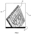
- Figure 4 is a photographic perspective view of the waveguide structure of Figure 2 illustrating the double-sided etching of the waveguide structure;
- Figure 5 is a line drawing of the waveguide structure of Figure 2; and
- Figures 6a, 6b, 6c and 6d illustrates the fabrication steps for manufacture of the waveguide structure of Figures 2 and 3.
- The terahertz camera 1 of Figure 1 comprises an
X-Y stage 2 on which are mounted thescanning optics 3 and theterahertz detector 4 and aprocessor 5. The arrangement of thescanning optics 3 is conventional and comprises a plurality ofmirrors 6, 7, e.g. planar or parabolic or hyperbolic. Eachmirror 6, 7 is movably mounted on respectiveorthogonal tracks 8, 9 and arranged to direct incident radiation from a specimen on a fixed specimen support (not illustrated) to theterahertz detector 4. Relative movement of the twomirrors 6, 7 on their tracks thus enables the specimen to be scanned in orthogonal directions. The scanning may be effected otherwise, e.g. by means of rotating or flipping mirrors. - It will, of course, be appreciated that the
mirrors 6, 7 should exhibit a high reflectivity to the particular radiation in order to minimise losses especially where passive radiation of a specimen is being imaged as the power of such radiation can be of the order of 10-12W. - With the embodiment of a terahertz camera illustrated in Figure 1, movement of the two
mirrors 6, 7 is controlled by separatelinear motors 10, 11, which may be stepper motors to ensure precise positioning of the mirrors in the X-Y plane. Each of themotors 10, 11 includes adata port 12 that is connected to theprocessor 5 and feeds data on the instantaneous positions of the mirrors, and also receives control signals from the computer. As previously stated, flipping mirrors or else may be use for scanning. - The
terahertz detector 4 is coupled to an intermediate frequency IFelectronic circuit 28 and to a basebandelectronic circuit 29 which has anoutput data port 13 in communication with thecontroller 5. Thecontroller 5, which is preferably a conventional desktop or portable computer, receives and synchronises the image data from thedetector 4 and the positional data from the drivers of themotors 10, 11 and builds from the data an image of the scanned specimen. Conventional data acquisition software may be used for this purpose. This image may be displayed on a screen and/or output to a printer as well as being stored as a conventional file. In Figure 2, theterahertz detector 4 is illustrated in detail. Its components are fabricated in or are mounted on a semi-conductor, e.g. silicon structure an example of which is illustrated in Figures 3 and 4. Alternatively, a metallic structure may be used. The components of thedetector 4 comprise an antenna comprised of ahorn antenna 14 and awaveguide 15, amixer 16 and alocal oscillator feed 17. The antenna selectively receives a predetermined frequency of electromagnetic radiation ("signal input"), thewaveguide 15 being in communication with amixer 16 which is also in communication with alocal oscillator feed 17 comprised of a waveguide structure and having a signal input for connection to a local oscillator. Themixer 16 heterodyns the signal input and the local oscillator input so as to generate an intermediate frequency ("IF") output. In other words, in this embodiment of an IF signal is generated in the detector rather than outside as in Figure 1. Themixer 16 includes on a microstrip a firstpass band filter 18 for isolating the local oscillator input from thewaveguide 15 and a secondpass band filter 19 which acts as a back stop to allow through only the pre-selected IF output. - As can be seen in the Figures, the
mixer 16 is arranged so as to be substantially orthogonal to thewaveguide 15. However, the intersection of the axis of themixer 16 with the axis of thelocal oscillator feed 17 is not orthogonal and instead describes an acute angle. This arrangement of the local oscillator feed 17 at an acute angle to themixer 16 reduces the back short length over a wider band width and so improves the bandwidth of the mixer transition in comparison to the more conventional 90° arrangement. Moreover, this arrangement of thelocal oscillator input 17 and themixer 16 provides an added benefit particular to imaging systems at these frequencies. It reduces the space occupied by each detector, thereby allowing them to be placed closer and a larger number of them, improving the resolution of the camera. - The illustrated
detector 4 is comprised for example of sixteen separate horn antenna providing a two-colour, eight pixel array. The size of the aperture of thedetector 4 required to generate images at terahertz frequencies is such that the spacing between the individual horn antennae is limited to approximately 2.5 mm in the illustrated example. This spacing is not sufficient to enable the more conventional arrangement of the mixer at 90° to the local oscillator feed and so the detector aperture presents a limit to the number of antenna. However, by arranging the axis of the localoscillator input feed 17 so that it is substantially aligned with the axis of theantenna horn 14 and arranging the intersection of the axis of the mixer and the local oscillator feed 17 at 45° the number of detectors may be increased in the same area thereby improving the resolution of the detector. - It will, of course, be appreciated that whilst the illustrated arrangement of the
mixer 16 andlocal oscillator feed 17 is preferred especially where the detector consists of an array of antennae in order to increase resolution, the terahertz imaging system describe herein is intended to also encompass more conventional arrangements of mixer and local oscillator feed. - As mentioned earlier, the
detector 4 is fabricated from a semi conductor, e.g. silicon structure consisting of three separate etched layers: atop layer 23, amiddle layer 20 and alower layer 24 which are illustrated in Figure 1. Figures 3 and 4 show themiddle layer 20 which is etched on both itsupper surface 21 and itslower surface 22. Theupper layer 23 and thelower layer 24 are each etched on only one side and the pattern of the etch in each case is a mirror image of the etch pattern of the respectiveupper surface 21 andlower surface 22 of themiddle layer 20. Thus, whilst for each individual layer of silicon the etch pattern is open, when the three layers are brought together, the etch patterns of their surfaces match to define waveguide structures extending along the interface of the surfaces. Cooperating location holes andpins 25 are also provided in the surfaces of each of the layers to ensure accurate positioning of the layers with respect to one another. - With reference to the
middle layer 20, illustrated in Figures 3 and 4, eight separate horn antennae are shown on theupper surface 21 of themiddle layer 20. In Figure 4 the outline of a second row of eight horn antennae on the opposedlower surface 22 of themiddle layer 20 can also been seen. Eachhorn antenna 14 is individually connected to itsrespective waveguide 15 andmixer 16. Individual local oscillator feeds 17 connect withrespective mixers 16 but are themselves interconnected with one another upstream from the mixers to a single commonlocal oscillator input 26. Thus, there are two separatelocal oscillator inputs 26, one for each surface of the middle layer 20 (for each set of eight antennae) and preferably, these twoinputs 26 emerge at the edge of themiddle layer 20 at different locations for ease of connection to the local oscillator source (not illustrated). - The dimensions of the etch pattern defining the waveguide structure are important to the functioning of the
detector 4 and these dimensions can be determined though conventional modelling techniques. The detector illustrated in the figures is a two-colour detector with one of the set of eight antenna detecting a first terahertz frequency and the parallel second set of eight antenna detecting a second, different, terahertz frequency. This in turn requires the dimensions of the etch pattern for each of the two sets of eight antenna to differ slightly depending upon the frequencies of the input signal and the local oscillator signal. Moreover, to maximise structural strength, it can be seen in Figure 4 that each row of horn antennae are offset from one another. The following measurements in relation to Figure 5 are therefore provided solely to illustrate typical dimensions.Table 1 Element Structure Antenna Row 1 (mm) Antenna Row 2 (mm) a - Layer thickness 2.4 2.4 b - Layer width 25 25 c - Layer length 29 29 d - Cone angle of horn 23.5 ° 27.7° e - width of horn aperture 0.78 1.04 f - Width of signal input tuning circuit 0.1 3 g - distance of first branch of local oscillator feed from edge 12.74 11.62 h - distance of second branch of local oscillator feed from edge 7.86 6.62 i - distance of third branch of local oscillator feed from edge 5.36 4.42 j - Width of local oscillator feed adjacent mixer 0.39 0.43 - Downstream of the
mixer 16, the IF output for each antenna passes to an outer surface of the silicon layered structure along a wire extending through a respective via 27. Thus a series of eight IF output vias extend through the body of thetop silicon layer 23 and a corresponding series of eight IF output vias extend through the body of thebottom silicon layer 24. From there the IF outputs pass through a conventional series of 2stage amplifiers 28 to anintegrated detector 29 and from there to the data input port of theprocessor 5. - For detection of passive radiation at 250GHz, for example a local oscillator signal of 245 GHz may be used to extracted an IF signal at 5 GHZ. It is to be understood that the frequencies quoted above are one illustration only and that conventional heterodyne theory can be employed to identify other suitable local oscillator frequencies and IF frequencies.
- With the detector described above, passive radiation at terahertz frequencies can be detected at room temperature and the use of a heterodyne receiver ensures a spectrally specific and sensitive detector. Although a two-colour eight pixel array is described, it is immediately apparent that a single antenna terahertz camera comprising only two layers of patterned silicon may be implemented in the manner described above. Moreover, further layers of patterned silicon may be added with in each case the common
local oscillator input 26 being located at different positions along the periphery of the silicon layers. However, where more than two rows of antenna are provided, the IF output vias must pass through intermediate silicon layers, avoiding the waveguide structure of that layer, and so the patterning of the antennae for different antennae rows should be offset from each other. - Of course, the number of antennas in a row may be different from 8, and there may be more than 8 antennas in a row.
- Furthermore, it is envisaged that rather than using a slab of metallized intrinsic silicon or metal for the fabrication of the individual waveguide structures, the antennae may be fabricated in photonic bandgap material. This would prevent signal leakage between adjacent antennae and could provide an alternative structure for the mixer and for the conduction of both the signal input, the local oscillator LO signal and the intermediate frequency IF output.
- The waveguide structure described above requires etching of the individual silicon layers and a novel method of fabricating these structures is described below. With reference to Figure 6a a
silicon substrate 30 is illustrated on the upper surface of which is provided a series of threemasks uppermost mask 31 is a positive resist or a metal mask. Directly beneath the first mask is a second negative resistmask 32 such as SU8 or other suitable amide mask material. Beneath the second mask is athird mask 33 preferably of silicon dioxide or aluminium nitride. Thefirst mask 31 defines the deepest structures in the substrate and protects other areas from early etching. The second mask exposes, in addition to the deepest etch regions, intermediate depth etch regions whilst protecting those regions of the substrate that require the shallowest etch. The third and final mask exposes all areas previously etched as well as those areas requiring the shallowest etch. It is worth noting that the masks are not necessarily laid one on top of the next, but may be brought separately. - With regard to the waveguide structure described above, the deepest etches are patterned for the
horn antennas 14 and thewaveguides 15, the intermediate etch depth is required for the majority of the local oscillator waveguide structure and then the shallowest etching is required for the mixer channel. Once all of the individual masks have been applied, the first etch is performed using the positive resistmask 31. The etch is continued to an etch depth equivalent to the difference between the desired final depth of the deepest structures and the final depth of the intermediate structures. The positive resistmask 31 is then removed (Figure 6b) using a normal stripper such as an amine type stripper which does not affect the underlying negative resistmask 32. The next etch stage is then performed through theSU8 mask 32 to a depth equivalent to the difference between the desired final depth of the intermediate structures and the shallowest structures. As the etched pattern from the first etch stage remain exposed this pattern is again etched and the pattern driven deeper into the substrate. Once the second etch is completed thesecond mask 32 is removed (Figure 6c) which does not affect the underlyingthird mask 33 and then the third and final etch stage can be performed during which the shallowest features of the pattern are etched and the existing pattern again etched more deeply into thesubstrate 30 to its final depth. Thethird mask 33 is then removed (Figure 6d). This procedure differs from then conventional procedure as it involves the use of a plurality of different masks each directly overlying an adjacent mask and an etching procedure in which new masks are not applied to the surface of the wafer in between etching steps. - Afterwards, the silicon is metallised in the desired regions (waveguides and vias)
- Although reference has been made herein to the use of a convention X-Y stage for scanning a specimen by means of a static terahertz camera and mobile scanning optics it will, of course, be apparent that alternatives to this arrangement are envisaged. For example, the specimen may be mounted on an X-Y stage and moved so that different areas of the specimen are scanned in turn.
- Alternatively, scanning may be performed wholly electronically through adjustment of the phase of the local oscillator input In this regard a phase shifter may be introduced into the individual local oscillator feeds 17. As is known, the phase shifter is comprised of a waveguide which has a slab of high resistivity intrinsic silicon mounted on the inside of one wall of the waveguide. The slab of silicon is exposed to incident light which causes the silicon to exhibit resistive and/or metallic properties. The power of the incident light determines the depth to which the changes in the silicon penetrate, changing the dimensions of the waveguide and thereby its dispersion characteristics.
- The imaging device described herein is suitable for the detection of passive millimeter and sub-millimeter electromagnetic radiation and in this respect is particularly convenient in view of its compact size, potential for portability and its ability to perform at room temperature. Thus, immediate applications for the imaging device are envisaged in both airborne and land vehicles, in security systems, in the chemical and food industries and in medical diagnostics. However, the scope of applications is not limited to those identified above and because of the low power requirements of the imaging system, it is particularly suited for example to imaging from space.
Claims (13)
- An imaging device to be used with millimeter and/or sub-millimeter radiation comprising at least a pair of substrates (20, 23, 24, 30), at least one of which is patterned on at least one surface with a patterning defining at least one radiation detector (4), each radiation detector comprising :- an antenna (14) adapted to receive millimeter and/or sub-millimeter electromagnetic radiation,- a mixer channel (16) coupled to said antenna and in communication with a via extending through a substrate for connection to a signal output,characterized by a mixer comprising filters (18, 19) mounted in the mixer channel for extracting an intermediate frequency signal in dependence upon said radiation received by the antenna,- and by a waveguide structure (17) coupled to said mixer and having a signal input for connection to a local oscillator, wherein the mixer channel intersects the local oscillator waveguide at an acute angle.
- An imaging device as in claim 1, wherein each substrate of the said pair of substrates is patterned on at least one surface with complementary patterning defining in combination said radiation detector.
- The imaging device as in claim 1 or 2, wherein said patterning defines a plurality of radiation detectors (4).
- The imaging device as in any one of claims 1 to 3, wherein it comprises at least a third substrate, said three substrates defining two rows of radiation detectors.
- The imaging device as in any one of claims 1 to 4, wherein the antenna is comprised of a horn (14) and of an antenna waveguide (15) that is coupled to said hom (14) and that intersects the mixer channel (16) substantially orthogonally.
- An imaging device as in claim 5, wherein the antenna waveguide is offset from the hom axis by an acute angle.
- The imaging device as in claim 6, wherein the local oscillator waveguide is parallel to the horn axis.
- A process for making a patterned substrate for an imaging device to be used with millimeter and/or sub-millimeter radiation comprising at least a pair of substrates (20, 23, 24, 30), at least one of which is patterned on at least one surface with a patterning defining at least one radiation detector (4), each radiation detector comprising :- an antenna (14) adapted to receive millimeter and/or sub-millimeter electromagnetic radiation,- a mixer channel (16) coupled to said antenna and in communication with a via extending through a substrate for connection to a signal output, a mixer comprising filters (18, 19) being mounted in the mixer channel for extracting an intermediate frequency signal in dependence upon said radiation received by the antenna,- a waveguide structure (17) coupled to said mixer and having a signal input for connection to a local oscillator, said process comprising the following steps:- providing on a surface of a substrate a first (31), a second (32) and a third patterned mask (33), said first mask (31) having a first pattern corresponding to a first region of each radiation detector with the highest etch depth, said second mask (32) having a second pattern corresponding to said first region and to a second region of each radiation detector with intermediate etch depth, and said third mask (33) having a third pattern corresponding to said first and second regions and to a third region of each radiation detectors with the shallowest etch depth.- performing a first etch through the first pattern of the first mask (31) at a first depth that is substantially equal to the difference between the highest etch depth and the intermediate etch depth.- removing said first mask (31)- performing a second etch through the second pattern of the second mask (32) at a second depth that is substantially equal to the difference between the intermediate etch depth and the shallowest etch depth.- removing said second mask (32)- performing a third etch through the third pattern of the third mask (33) with an etch depth that is substantively equal to the shallowest etch depth removing said third mask (33).
- A process as in claim 8, wherein said first (31), second (32) and third (33) masks are each laid on top of the next and in direct contact with the adjacent mask.
- A process as in claim 9, wherein one of said masks (31, 32, 33) is a positive resist, or a metal mask, wherein another mask is a negative resist mask or an amid mask, and yet another mask is of silicon dioxide or aluminium nitride.
- A process as in claim 8 or 9, wherein said first region corresponds to said antenna.
- A process as in any one of claims 9 to 11, wherein said second region corresponds to at least part of said waveguide structure.
- A process as in any one of claims 9 to 12, wherein said second region corresponds to said mixer channel.
Applications Claiming Priority (3)
| Application Number | Priority Date | Filing Date | Title |
|---|---|---|---|
| GBGB0224912.6A GB0224912D0 (en) | 2002-10-25 | 2002-10-25 | Sub-millimetre wavelength camera |
| GB0224912 | 2002-10-25 | ||
| PCT/EP2003/013342 WO2004038854A2 (en) | 2002-10-25 | 2003-10-27 | Sub-millimetre wavelength camera |
Publications (2)
| Publication Number | Publication Date |
|---|---|
| EP1554780A2 EP1554780A2 (en) | 2005-07-20 |
| EP1554780B1 true EP1554780B1 (en) | 2007-04-18 |
Family
ID=9946612
Family Applications (1)
| Application Number | Title | Priority Date | Filing Date |
|---|---|---|---|
| EP03778333A Expired - Lifetime EP1554780B1 (en) | 2002-10-25 | 2003-10-27 | Sub-millimeter wavelength camera |
Country Status (13)
| Country | Link |
|---|---|
| US (1) | US7502605B2 (en) |
| EP (1) | EP1554780B1 (en) |
| JP (1) | JP4516426B2 (en) |
| KR (1) | KR100989846B1 (en) |
| CN (1) | CN1726618B (en) |
| AT (1) | ATE360271T1 (en) |
| AU (1) | AU2003285345A1 (en) |
| CA (1) | CA2503556A1 (en) |
| DE (1) | DE60313352T2 (en) |
| DK (1) | DK1554780T3 (en) |
| ES (1) | ES2285216T3 (en) |
| GB (1) | GB0224912D0 (en) |
| WO (1) | WO2004038854A2 (en) |
Families Citing this family (24)
| Publication number | Priority date | Publication date | Assignee | Title |
|---|---|---|---|---|
| US7521680B1 (en) * | 2003-12-05 | 2009-04-21 | Eric Dean Rosenthal | Electromagnetic spectral-based imaging devices and methods |
| US8311616B2 (en) | 2005-05-26 | 2012-11-13 | Yissum Research Development Company Of The Hebrew University Of Jerusalem | Method and system for determination of physiological conditions and emotional states of a living organism |
| GB0511209D0 (en) | 2005-06-02 | 2005-07-06 | Thru Vision Ltd | Scanning method and apparatus |
| GB0603193D0 (en) * | 2006-02-16 | 2006-03-29 | Thruvision Ltd | Detection method and apparatus |
| US7873329B2 (en) | 2006-04-25 | 2011-01-18 | ThruVision Systems Limited | Transceiver having mixer/filter within receiving/transmitting cavity |
| JP2009534976A (en) | 2006-04-25 | 2009-09-24 | スルビジョン リミティド | Feed horn assembly and manufacturing method thereof |
| US7764324B2 (en) * | 2007-01-30 | 2010-07-27 | Radiabeam Technologies, Llc | Terahertz camera |
| DE102007007378B3 (en) * | 2007-02-12 | 2008-04-17 | Genesis Adaptive Systeme Deutschland Gmbh | Terahertz measuring arrangement, has measuring device provided subsequent to optical amplifier in object optical path with terahertz-detector, and wave front sensor and switching unit supplying radiation to terahertz-detector |
| DE102007011704A1 (en) | 2007-03-08 | 2008-09-11 | Genesis Adaptive Systeme Deutschland Gmbh | Measuring device for mapping object area with terahertz radiation, has reference object arranged in object area, in which reference object is radiated by reference radiation |
| US7888646B2 (en) * | 2007-06-04 | 2011-02-15 | Morpho Detection, Inc. | System and method for detecting contraband |
| WO2009013681A1 (en) * | 2007-07-25 | 2009-01-29 | Koninklijke Philips Electronics N.V. | Integrated all-electronic terahertz imaging/spectroscopy device |
| US7745792B2 (en) * | 2007-08-15 | 2010-06-29 | Morpho Detection, Inc. | Terahertz detectors for use in terahertz inspection or imaging systems |
| JP5144175B2 (en) * | 2007-08-31 | 2013-02-13 | キヤノン株式会社 | Inspection apparatus and inspection method using electromagnetic waves |
| US9157852B2 (en) | 2010-09-17 | 2015-10-13 | Raytheon Company | Explosive material detection |
| WO2012094051A2 (en) | 2010-10-26 | 2012-07-12 | California Institute Of Technology | Travelling wave distributed active antenna radiator structures, high frequency power generation and quasi-optical filtering |
| US9268017B2 (en) | 2011-07-29 | 2016-02-23 | International Business Machines Corporation | Near-field millimeter wave imaging |
| US8658976B2 (en) | 2011-12-01 | 2014-02-25 | California Institute Of Technology | Integrated terahertz imaging systems |
| GB2499380A (en) * | 2012-02-06 | 2013-08-21 | Digital Barriers Services Ltd | Multiple frequency terahertz imaging system |
| WO2014099822A2 (en) | 2012-12-17 | 2014-06-26 | Brady Patrick K | System and method for identifying materials using a thz spectral fingerprint in a media with high water content |
| US9494464B2 (en) * | 2013-02-20 | 2016-11-15 | Battelle Energy Alliance, Llc | Terahertz imaging devices and systems, and related methods, for detection of materials |
| CN106603015A (en) * | 2016-12-29 | 2017-04-26 | 中国科学院国家空间科学中心 | Terahertz mixer realizing short baseline measurement and front-end of receiver |
| US20200081433A1 (en) * | 2018-09-12 | 2020-03-12 | International Business Machines Corporation | Self-Driving Security Checking and Boarding Vehicle System |
| KR20220079666A (en) * | 2019-10-17 | 2022-06-13 | 쓰루비젼 엘티디 | High frequency detection method and device |
| IL292207B2 (en) * | 2019-10-17 | 2026-03-01 | Thruvision Ltd | High frequency heterodyne mixer |
Family Cites Families (9)
| Publication number | Priority date | Publication date | Assignee | Title |
|---|---|---|---|---|
| US4641369A (en) * | 1984-11-29 | 1987-02-03 | Trw Inc. | Local oscillator and mixer assembly |
| US4607394A (en) * | 1985-03-04 | 1986-08-19 | General Electric Company | Single balanced planar mixer |
| GB9603196D0 (en) * | 1996-02-15 | 1996-04-17 | Council Cent Lab Res Councils | Waveguide structures and a method of fabrication thereof |
| US6323818B1 (en) * | 1997-03-25 | 2001-11-27 | University Of Virginia Patent Foundation | Integration of hollow waveguides, channels and horns by lithographic and etching techniques |
| AU6772998A (en) * | 1997-03-25 | 1998-10-20 | University Of Virginia Patent Foundation | Method of fabricating a millimeter or submillimeter wavelength component |
| US6404402B1 (en) * | 1997-03-25 | 2002-06-11 | University Of Virginia Patent Foundation | Preferential crystal etching technique for the fabrication of millimeter and submillimeter wavelength horn antennas |
| JP3760051B2 (en) * | 1998-08-04 | 2006-03-29 | シャープ株式会社 | Frequency adjusting device for NRD guide millimeter wave oscillator |
| US6522304B2 (en) * | 2001-04-11 | 2003-02-18 | International Business Machines Corporation | Dual damascene horn antenna |
| JP3954380B2 (en) * | 2001-12-28 | 2007-08-08 | 株式会社東芝 | Imaging device |
-
2002
- 2002-10-25 GB GBGB0224912.6A patent/GB0224912D0/en not_active Ceased
-
2003
- 2003-10-27 CN CN200380106120.XA patent/CN1726618B/en not_active Expired - Lifetime
- 2003-10-27 AU AU2003285345A patent/AU2003285345A1/en not_active Abandoned
- 2003-10-27 DE DE60313352T patent/DE60313352T2/en not_active Expired - Lifetime
- 2003-10-27 CA CA002503556A patent/CA2503556A1/en not_active Abandoned
- 2003-10-27 DK DK03778333T patent/DK1554780T3/en active
- 2003-10-27 JP JP2004546033A patent/JP4516426B2/en not_active Expired - Lifetime
- 2003-10-27 AT AT03778333T patent/ATE360271T1/en not_active IP Right Cessation
- 2003-10-27 US US10/532,736 patent/US7502605B2/en not_active Expired - Lifetime
- 2003-10-27 KR KR1020057007155A patent/KR100989846B1/en not_active Expired - Lifetime
- 2003-10-27 WO PCT/EP2003/013342 patent/WO2004038854A2/en not_active Ceased
- 2003-10-27 ES ES03778333T patent/ES2285216T3/en not_active Expired - Lifetime
- 2003-10-27 EP EP03778333A patent/EP1554780B1/en not_active Expired - Lifetime
Non-Patent Citations (1)
| Title |
|---|
| None * |
Also Published As
| Publication number | Publication date |
|---|---|
| DK1554780T3 (en) | 2007-09-17 |
| DE60313352D1 (en) | 2007-05-31 |
| EP1554780A2 (en) | 2005-07-20 |
| HK1077127A1 (en) | 2006-02-03 |
| KR100989846B1 (en) | 2010-10-29 |
| CN1726618B (en) | 2011-07-06 |
| US7502605B2 (en) | 2009-03-10 |
| JP2006505157A (en) | 2006-02-09 |
| WO2004038854A3 (en) | 2004-06-17 |
| JP4516426B2 (en) | 2010-08-04 |
| AU2003285345A8 (en) | 2004-05-13 |
| ATE360271T1 (en) | 2007-05-15 |
| CA2503556A1 (en) | 2004-05-06 |
| CN1726618A (en) | 2006-01-25 |
| US20060111619A1 (en) | 2006-05-25 |
| KR20050088405A (en) | 2005-09-06 |
| AU2003285345A1 (en) | 2004-05-13 |
| ES2285216T3 (en) | 2007-11-16 |
| DE60313352T2 (en) | 2008-01-03 |
| GB0224912D0 (en) | 2002-12-04 |
| WO2004038854A2 (en) | 2004-05-06 |
Similar Documents
| Publication | Publication Date | Title |
|---|---|---|
| US7502605B2 (en) | Sub-millimeter wavelength camera | |
| JP2022062063A (en) | Antenna array | |
| US11316280B2 (en) | Tiling system and method for an array antenna | |
| DE69833716T2 (en) | Transparent planar antenna structure | |
| DE102022204159A1 (en) | ELECTRONIC DEVICES WITH ISOLATED ANTENNA MODULES | |
| US8305259B2 (en) | Dual-band antenna array and RF front-end for mm-wave imager and radar | |
| EP1723696B1 (en) | Tunable arrangements | |
| DE60318075T2 (en) | REAL TIME MILLIMETER WAVE IMAGING SYSTEM USING CROSS CORRELATION | |
| DE69412264T2 (en) | RADIATION SENSOR | |
| DE102021203692A1 (en) | ELECTRONIC DEVICES WITH DIELECTRIC RESONATOR ANTENNAS WITH PARASITARY PATCHES | |
| DE112018002681T5 (en) | ANTENNAS IN STRUCTURED CONDUCTIVE LAYERS | |
| US11695207B2 (en) | Vehicle antenna device with side wall lens | |
| EP0386152A4 (en) | Millimeter wave imaging device | |
| JPH10153655A (en) | Millimeter wave imaging system | |
| US20190369200A1 (en) | Radiovision device | |
| US5237334A (en) | Focal plane antenna array for millimeter waves | |
| DE102020103778A1 (en) | INVERTED MICROSTRIP TRAVELING WAVE PATCH ARRAY ANTENNA SYSTEM | |
| US8885774B2 (en) | Receiving apparatus for high frequency imaging system | |
| DE102022209306A1 (en) | WIRELESS COMMUNICATION DEVICES | |
| US6762719B2 (en) | Self-orienting antenna array systems | |
| CN115313066B (en) | Phased array antenna device and phased array communication system | |
| DE102023208493A1 (en) | ELECTRONIC DEVICE HAVING A CONDUCTIVE CONTACT SOLDERED TO A PRINTED CIRCUIT | |
| HK1077127B (en) | Sub-millimetre wavelength camera | |
| DE10035623A1 (en) | Device for transmitting and / or receiving electromagnetic waves and method for producing the device | |
| JPH1168455A (en) | Quasi-optical antenna / mixer element and array type quasi-optical antenna / mixer |
Legal Events
| Date | Code | Title | Description |
|---|---|---|---|
| PUAI | Public reference made under article 153(3) epc to a published international application that has entered the european phase |
Free format text: ORIGINAL CODE: 0009012 |
|
| 17P | Request for examination filed |
Effective date: 20050518 |
|
| AK | Designated contracting states |
Kind code of ref document: A2 Designated state(s): AT BE BG CH CY CZ DE DK EE ES FI FR GB GR HU IE IT LI LU MC NL PT RO SE SI SK TR |
|
| AX | Request for extension of the european patent |
Extension state: AL LT LV MK |
|
| REG | Reference to a national code |
Ref country code: HK Ref legal event code: DE Ref document number: 1077127 Country of ref document: HK |
|
| DAX | Request for extension of the european patent (deleted) | ||
| GRAP | Despatch of communication of intention to grant a patent |
Free format text: ORIGINAL CODE: EPIDOSNIGR1 |
|
| RTI1 | Title (correction) |
Free format text: SUB-MILLIMETER WAVELENGTH CAMERA |
|
| GRAS | Grant fee paid |
Free format text: ORIGINAL CODE: EPIDOSNIGR3 |
|
| 17Q | First examination report despatched |
Effective date: 20050819 |
|
| GRAJ | Information related to disapproval of communication of intention to grant by the applicant or resumption of examination proceedings by the epo deleted |
Free format text: ORIGINAL CODE: EPIDOSDIGR1 |
|
| GRAP | Despatch of communication of intention to grant a patent |
Free format text: ORIGINAL CODE: EPIDOSNIGR1 |
|
| GRAS | Grant fee paid |
Free format text: ORIGINAL CODE: EPIDOSNIGR3 |
|
| GRAA | (expected) grant |
Free format text: ORIGINAL CODE: 0009210 |
|
| AK | Designated contracting states |
Kind code of ref document: B1 Designated state(s): AT BE BG CH CY CZ DE DK EE ES FI FR GB GR HU IE IT LI LU MC NL PT RO SE SI SK TR |
|
| PG25 | Lapsed in a contracting state [announced via postgrant information from national office to epo] |
Ref country code: LI Free format text: LAPSE BECAUSE OF FAILURE TO SUBMIT A TRANSLATION OF THE DESCRIPTION OR TO PAY THE FEE WITHIN THE PRESCRIBED TIME-LIMIT Effective date: 20070418 Ref country code: SI Free format text: LAPSE BECAUSE OF FAILURE TO SUBMIT A TRANSLATION OF THE DESCRIPTION OR TO PAY THE FEE WITHIN THE PRESCRIBED TIME-LIMIT Effective date: 20070418 Ref country code: FI Free format text: LAPSE BECAUSE OF FAILURE TO SUBMIT A TRANSLATION OF THE DESCRIPTION OR TO PAY THE FEE WITHIN THE PRESCRIBED TIME-LIMIT Effective date: 20070418 Ref country code: CH Free format text: LAPSE BECAUSE OF FAILURE TO SUBMIT A TRANSLATION OF THE DESCRIPTION OR TO PAY THE FEE WITHIN THE PRESCRIBED TIME-LIMIT Effective date: 20070418 |
|
| REG | Reference to a national code |
Ref country code: CH Ref legal event code: EP |
|
| REG | Reference to a national code |
Ref country code: IE Ref legal event code: FG4D |
|
| REF | Corresponds to: |
Ref document number: 60313352 Country of ref document: DE Date of ref document: 20070531 Kind code of ref document: P |
|
| REG | Reference to a national code |
Ref country code: SE Ref legal event code: TRGR |
|
| ET | Fr: translation filed | ||
| REG | Reference to a national code |
Ref country code: DK Ref legal event code: T3 |
|
| PG25 | Lapsed in a contracting state [announced via postgrant information from national office to epo] |
Ref country code: PT Free format text: LAPSE BECAUSE OF FAILURE TO SUBMIT A TRANSLATION OF THE DESCRIPTION OR TO PAY THE FEE WITHIN THE PRESCRIBED TIME-LIMIT Effective date: 20070918 |
|
| REG | Reference to a national code |
Ref country code: CH Ref legal event code: PL |
|
| REG | Reference to a national code |
Ref country code: ES Ref legal event code: FG2A Ref document number: 2285216 Country of ref document: ES Kind code of ref document: T3 |
|
| PG25 | Lapsed in a contracting state [announced via postgrant information from national office to epo] |
Ref country code: AT Free format text: LAPSE BECAUSE OF FAILURE TO SUBMIT A TRANSLATION OF THE DESCRIPTION OR TO PAY THE FEE WITHIN THE PRESCRIBED TIME-LIMIT Effective date: 20070418 |
|
| REG | Reference to a national code |
Ref country code: HK Ref legal event code: GR Ref document number: 1077127 Country of ref document: HK |
|
| PG25 | Lapsed in a contracting state [announced via postgrant information from national office to epo] |
Ref country code: BE Free format text: LAPSE BECAUSE OF FAILURE TO SUBMIT A TRANSLATION OF THE DESCRIPTION OR TO PAY THE FEE WITHIN THE PRESCRIBED TIME-LIMIT Effective date: 20070418 |
|
| PG25 | Lapsed in a contracting state [announced via postgrant information from national office to epo] |
Ref country code: CZ Free format text: LAPSE BECAUSE OF FAILURE TO SUBMIT A TRANSLATION OF THE DESCRIPTION OR TO PAY THE FEE WITHIN THE PRESCRIBED TIME-LIMIT Effective date: 20070418 Ref country code: BG Free format text: LAPSE BECAUSE OF FAILURE TO SUBMIT A TRANSLATION OF THE DESCRIPTION OR TO PAY THE FEE WITHIN THE PRESCRIBED TIME-LIMIT Effective date: 20070718 |
|
| PLBE | No opposition filed within time limit |
Free format text: ORIGINAL CODE: 0009261 |
|
| STAA | Information on the status of an ep patent application or granted ep patent |
Free format text: STATUS: NO OPPOSITION FILED WITHIN TIME LIMIT |
|
| PG25 | Lapsed in a contracting state [announced via postgrant information from national office to epo] |
Ref country code: SK Free format text: LAPSE BECAUSE OF FAILURE TO SUBMIT A TRANSLATION OF THE DESCRIPTION OR TO PAY THE FEE WITHIN THE PRESCRIBED TIME-LIMIT Effective date: 20070418 |
|
| 26N | No opposition filed |
Effective date: 20080121 |
|
| PG25 | Lapsed in a contracting state [announced via postgrant information from national office to epo] |
Ref country code: GR Free format text: LAPSE BECAUSE OF FAILURE TO SUBMIT A TRANSLATION OF THE DESCRIPTION OR TO PAY THE FEE WITHIN THE PRESCRIBED TIME-LIMIT Effective date: 20070719 |
|
| PG25 | Lapsed in a contracting state [announced via postgrant information from national office to epo] |
Ref country code: RO Free format text: LAPSE BECAUSE OF FAILURE TO SUBMIT A TRANSLATION OF THE DESCRIPTION OR TO PAY THE FEE WITHIN THE PRESCRIBED TIME-LIMIT Effective date: 20070418 Ref country code: MC Free format text: LAPSE BECAUSE OF NON-PAYMENT OF DUE FEES Effective date: 20071031 |
|
| PG25 | Lapsed in a contracting state [announced via postgrant information from national office to epo] |
Ref country code: IE Free format text: LAPSE BECAUSE OF NON-PAYMENT OF DUE FEES Effective date: 20071030 |
|
| PG25 | Lapsed in a contracting state [announced via postgrant information from national office to epo] |
Ref country code: EE Free format text: LAPSE BECAUSE OF FAILURE TO SUBMIT A TRANSLATION OF THE DESCRIPTION OR TO PAY THE FEE WITHIN THE PRESCRIBED TIME-LIMIT Effective date: 20070418 |
|
| PG25 | Lapsed in a contracting state [announced via postgrant information from national office to epo] |
Ref country code: CY Free format text: LAPSE BECAUSE OF FAILURE TO SUBMIT A TRANSLATION OF THE DESCRIPTION OR TO PAY THE FEE WITHIN THE PRESCRIBED TIME-LIMIT Effective date: 20070418 |
|
| PG25 | Lapsed in a contracting state [announced via postgrant information from national office to epo] |
Ref country code: LU Free format text: LAPSE BECAUSE OF NON-PAYMENT OF DUE FEES Effective date: 20071027 |
|
| PG25 | Lapsed in a contracting state [announced via postgrant information from national office to epo] |
Ref country code: TR Free format text: LAPSE BECAUSE OF FAILURE TO SUBMIT A TRANSLATION OF THE DESCRIPTION OR TO PAY THE FEE WITHIN THE PRESCRIBED TIME-LIMIT Effective date: 20070418 Ref country code: HU Free format text: LAPSE BECAUSE OF FAILURE TO SUBMIT A TRANSLATION OF THE DESCRIPTION OR TO PAY THE FEE WITHIN THE PRESCRIBED TIME-LIMIT Effective date: 20071019 |
|
| PGFP | Annual fee paid to national office [announced via postgrant information from national office to epo] |
Ref country code: DK Payment date: 20101015 Year of fee payment: 8 Ref country code: NL Payment date: 20101013 Year of fee payment: 8 |
|
| PGFP | Annual fee paid to national office [announced via postgrant information from national office to epo] |
Ref country code: SE Payment date: 20101014 Year of fee payment: 8 |
|
| REG | Reference to a national code |
Ref country code: NL Ref legal event code: V1 Effective date: 20120501 |
|
| REG | Reference to a national code |
Ref country code: DK Ref legal event code: EBP |
|
| REG | Reference to a national code |
Ref country code: SE Ref legal event code: EUG |
|
| PG25 | Lapsed in a contracting state [announced via postgrant information from national office to epo] |
Ref country code: NL Free format text: LAPSE BECAUSE OF NON-PAYMENT OF DUE FEES Effective date: 20120501 |
|
| PG25 | Lapsed in a contracting state [announced via postgrant information from national office to epo] |
Ref country code: DK Free format text: LAPSE BECAUSE OF NON-PAYMENT OF DUE FEES Effective date: 20111031 Ref country code: SE Free format text: LAPSE BECAUSE OF NON-PAYMENT OF DUE FEES Effective date: 20111028 |
|
| REG | Reference to a national code |
Ref country code: FR Ref legal event code: PLFP Year of fee payment: 13 |
|
| REG | Reference to a national code |
Ref country code: FR Ref legal event code: PLFP Year of fee payment: 14 |
|
| REG | Reference to a national code |
Ref country code: FR Ref legal event code: PLFP Year of fee payment: 15 |
|
| REG | Reference to a national code |
Ref country code: FR Ref legal event code: PLFP Year of fee payment: 16 |
|
| PGFP | Annual fee paid to national office [announced via postgrant information from national office to epo] |
Ref country code: FR Payment date: 20221028 Year of fee payment: 20 |
|
| PGFP | Annual fee paid to national office [announced via postgrant information from national office to epo] |
Ref country code: IT Payment date: 20221026 Year of fee payment: 20 Ref country code: GB Payment date: 20221019 Year of fee payment: 20 Ref country code: ES Payment date: 20221222 Year of fee payment: 20 Ref country code: DE Payment date: 20220620 Year of fee payment: 20 |
|
| REG | Reference to a national code |
Ref country code: DE Ref legal event code: R071 Ref document number: 60313352 Country of ref document: DE |
|
| REG | Reference to a national code |
Ref country code: ES Ref legal event code: FD2A Effective date: 20231106 |
|
| REG | Reference to a national code |
Ref country code: GB Ref legal event code: PE20 Expiry date: 20231026 |
|
| PG25 | Lapsed in a contracting state [announced via postgrant information from national office to epo] |
Ref country code: GB Free format text: LAPSE BECAUSE OF EXPIRATION OF PROTECTION Effective date: 20231026 |
|
| PG25 | Lapsed in a contracting state [announced via postgrant information from national office to epo] |
Ref country code: ES Free format text: LAPSE BECAUSE OF EXPIRATION OF PROTECTION Effective date: 20231028 |
|
| PG25 | Lapsed in a contracting state [announced via postgrant information from national office to epo] |
Ref country code: GB Free format text: LAPSE BECAUSE OF EXPIRATION OF PROTECTION Effective date: 20231026 Ref country code: ES Free format text: LAPSE BECAUSE OF EXPIRATION OF PROTECTION Effective date: 20231028 |