EP1553551A2 - Apparatus and method for operating flat panel display - Google Patents
Apparatus and method for operating flat panel display Download PDFInfo
- Publication number
- EP1553551A2 EP1553551A2 EP05000270A EP05000270A EP1553551A2 EP 1553551 A2 EP1553551 A2 EP 1553551A2 EP 05000270 A EP05000270 A EP 05000270A EP 05000270 A EP05000270 A EP 05000270A EP 1553551 A2 EP1553551 A2 EP 1553551A2
- Authority
- EP
- European Patent Office
- Prior art keywords
- current
- data
- charge
- difference
- current reference
- Prior art date
- Legal status (The legal status is an assumption and is not a legal conclusion. Google has not performed a legal analysis and makes no representation as to the accuracy of the status listed.)
- Withdrawn
Links
- 238000000034 method Methods 0.000 title claims description 22
- 230000001105 regulatory effect Effects 0.000 abstract description 3
- 238000005401 electroluminescence Methods 0.000 description 25
- 230000008901 benefit Effects 0.000 description 6
- 238000007599 discharging Methods 0.000 description 6
- 230000008859 change Effects 0.000 description 4
- 230000001276 controlling effect Effects 0.000 description 3
- 238000005286 illumination Methods 0.000 description 2
- 230000006866 deterioration Effects 0.000 description 1
- 238000010586 diagram Methods 0.000 description 1
- 230000000694 effects Effects 0.000 description 1
- 238000005516 engineering process Methods 0.000 description 1
- 239000004973 liquid crystal related substance Substances 0.000 description 1
- 238000012986 modification Methods 0.000 description 1
- 230000004048 modification Effects 0.000 description 1
- 230000004044 response Effects 0.000 description 1
- 230000007704 transition Effects 0.000 description 1
Images



Classifications
-
- G—PHYSICS
- G09—EDUCATION; CRYPTOGRAPHY; DISPLAY; ADVERTISING; SEALS
- G09G—ARRANGEMENTS OR CIRCUITS FOR CONTROL OF INDICATING DEVICES USING STATIC MEANS TO PRESENT VARIABLE INFORMATION
- G09G3/00—Control arrangements or circuits, of interest only in connection with visual indicators other than cathode-ray tubes
- G09G3/20—Control arrangements or circuits, of interest only in connection with visual indicators other than cathode-ray tubes for presentation of an assembly of a number of characters, e.g. a page, by composing the assembly by combination of individual elements arranged in a matrix no fixed position being assigned to or needed to be assigned to the individual characters or partial characters
- G09G3/2007—Display of intermediate tones
- G09G3/2011—Display of intermediate tones by amplitude modulation
-
- A—HUMAN NECESSITIES
- A47—FURNITURE; DOMESTIC ARTICLES OR APPLIANCES; COFFEE MILLS; SPICE MILLS; SUCTION CLEANERS IN GENERAL
- A47L—DOMESTIC WASHING OR CLEANING; SUCTION CLEANERS IN GENERAL
- A47L15/00—Washing or rinsing machines for crockery or tableware
- A47L15/0018—Controlling processes, i.e. processes to control the operation of the machine characterised by the purpose or target of the control
- A47L15/0047—Energy or water consumption, e.g. by saving energy or water
-
- A—HUMAN NECESSITIES
- A47—FURNITURE; DOMESTIC ARTICLES OR APPLIANCES; COFFEE MILLS; SPICE MILLS; SUCTION CLEANERS IN GENERAL
- A47L—DOMESTIC WASHING OR CLEANING; SUCTION CLEANERS IN GENERAL
- A47L15/00—Washing or rinsing machines for crockery or tableware
- A47L15/42—Details
- A47L15/4214—Water supply, recirculation or discharge arrangements; Devices therefor
-
- G—PHYSICS
- G09—EDUCATION; CRYPTOGRAPHY; DISPLAY; ADVERTISING; SEALS
- G09G—ARRANGEMENTS OR CIRCUITS FOR CONTROL OF INDICATING DEVICES USING STATIC MEANS TO PRESENT VARIABLE INFORMATION
- G09G3/00—Control arrangements or circuits, of interest only in connection with visual indicators other than cathode-ray tubes
- G09G3/20—Control arrangements or circuits, of interest only in connection with visual indicators other than cathode-ray tubes for presentation of an assembly of a number of characters, e.g. a page, by composing the assembly by combination of individual elements arranged in a matrix no fixed position being assigned to or needed to be assigned to the individual characters or partial characters
- G09G3/22—Control arrangements or circuits, of interest only in connection with visual indicators other than cathode-ray tubes for presentation of an assembly of a number of characters, e.g. a page, by composing the assembly by combination of individual elements arranged in a matrix no fixed position being assigned to or needed to be assigned to the individual characters or partial characters using controlled light sources
- G09G3/30—Control arrangements or circuits, of interest only in connection with visual indicators other than cathode-ray tubes for presentation of an assembly of a number of characters, e.g. a page, by composing the assembly by combination of individual elements arranged in a matrix no fixed position being assigned to or needed to be assigned to the individual characters or partial characters using controlled light sources using electroluminescent panels
- G09G3/32—Control arrangements or circuits, of interest only in connection with visual indicators other than cathode-ray tubes for presentation of an assembly of a number of characters, e.g. a page, by composing the assembly by combination of individual elements arranged in a matrix no fixed position being assigned to or needed to be assigned to the individual characters or partial characters using controlled light sources using electroluminescent panels semiconductive, e.g. using light-emitting diodes [LED]
- G09G3/3208—Control arrangements or circuits, of interest only in connection with visual indicators other than cathode-ray tubes for presentation of an assembly of a number of characters, e.g. a page, by composing the assembly by combination of individual elements arranged in a matrix no fixed position being assigned to or needed to be assigned to the individual characters or partial characters using controlled light sources using electroluminescent panels semiconductive, e.g. using light-emitting diodes [LED] organic, e.g. using organic light-emitting diodes [OLED]
- G09G3/3216—Control arrangements or circuits, of interest only in connection with visual indicators other than cathode-ray tubes for presentation of an assembly of a number of characters, e.g. a page, by composing the assembly by combination of individual elements arranged in a matrix no fixed position being assigned to or needed to be assigned to the individual characters or partial characters using controlled light sources using electroluminescent panels semiconductive, e.g. using light-emitting diodes [LED] organic, e.g. using organic light-emitting diodes [OLED] using a passive matrix
-
- A—HUMAN NECESSITIES
- A47—FURNITURE; DOMESTIC ARTICLES OR APPLIANCES; COFFEE MILLS; SPICE MILLS; SUCTION CLEANERS IN GENERAL
- A47L—DOMESTIC WASHING OR CLEANING; SUCTION CLEANERS IN GENERAL
- A47L2501/00—Output in controlling method of washing or rinsing machines for crockery or tableware, i.e. quantities or components controlled, or actions performed by the controlling device executing the controlling method
- A47L2501/06—Water heaters
-
- G—PHYSICS
- G09—EDUCATION; CRYPTOGRAPHY; DISPLAY; ADVERTISING; SEALS
- G09G—ARRANGEMENTS OR CIRCUITS FOR CONTROL OF INDICATING DEVICES USING STATIC MEANS TO PRESENT VARIABLE INFORMATION
- G09G2310/00—Command of the display device
- G09G2310/02—Addressing, scanning or driving the display screen or processing steps related thereto
- G09G2310/0243—Details of the generation of driving signals
- G09G2310/0248—Precharge or discharge of column electrodes before or after applying exact column voltages
-
- G—PHYSICS
- G09—EDUCATION; CRYPTOGRAPHY; DISPLAY; ADVERTISING; SEALS
- G09G—ARRANGEMENTS OR CIRCUITS FOR CONTROL OF INDICATING DEVICES USING STATIC MEANS TO PRESENT VARIABLE INFORMATION
- G09G2310/00—Command of the display device
- G09G2310/02—Addressing, scanning or driving the display screen or processing steps related thereto
- G09G2310/0264—Details of driving circuits
- G09G2310/027—Details of drivers for data electrodes, the drivers handling digital grey scale data, e.g. use of D/A converters
-
- G—PHYSICS
- G09—EDUCATION; CRYPTOGRAPHY; DISPLAY; ADVERTISING; SEALS
- G09G—ARRANGEMENTS OR CIRCUITS FOR CONTROL OF INDICATING DEVICES USING STATIC MEANS TO PRESENT VARIABLE INFORMATION
- G09G2330/00—Aspects of power supply; Aspects of display protection and defect management
- G09G2330/02—Details of power systems and of start or stop of display operation
- G09G2330/021—Power management, e.g. power saving
-
- G—PHYSICS
- G09—EDUCATION; CRYPTOGRAPHY; DISPLAY; ADVERTISING; SEALS
- G09G—ARRANGEMENTS OR CIRCUITS FOR CONTROL OF INDICATING DEVICES USING STATIC MEANS TO PRESENT VARIABLE INFORMATION
- G09G3/00—Control arrangements or circuits, of interest only in connection with visual indicators other than cathode-ray tubes
- G09G3/20—Control arrangements or circuits, of interest only in connection with visual indicators other than cathode-ray tubes for presentation of an assembly of a number of characters, e.g. a page, by composing the assembly by combination of individual elements arranged in a matrix no fixed position being assigned to or needed to be assigned to the individual characters or partial characters
-
- G—PHYSICS
- G09—EDUCATION; CRYPTOGRAPHY; DISPLAY; ADVERTISING; SEALS
- G09G—ARRANGEMENTS OR CIRCUITS FOR CONTROL OF INDICATING DEVICES USING STATIC MEANS TO PRESENT VARIABLE INFORMATION
- G09G3/00—Control arrangements or circuits, of interest only in connection with visual indicators other than cathode-ray tubes
- G09G3/20—Control arrangements or circuits, of interest only in connection with visual indicators other than cathode-ray tubes for presentation of an assembly of a number of characters, e.g. a page, by composing the assembly by combination of individual elements arranged in a matrix no fixed position being assigned to or needed to be assigned to the individual characters or partial characters
- G09G3/22—Control arrangements or circuits, of interest only in connection with visual indicators other than cathode-ray tubes for presentation of an assembly of a number of characters, e.g. a page, by composing the assembly by combination of individual elements arranged in a matrix no fixed position being assigned to or needed to be assigned to the individual characters or partial characters using controlled light sources
Definitions
- the present invention relates in general to a flat panel display, and more particularly, to an apparatus and method for operating a flat panel display.
- flat panel displays with reduced weight and volume.
- LCDs Liquid Crystal Displays
- FEDs Field Emission Displays
- PDPs Plasma Display Panels
- organic EL Electro Luminescence
- the organic EL display stands along among other LCDs for its many advantages including a thinner screen, faster response speed, superior visibility due to the self-luminescent characteristics, and larger viewing angle.
- Organic EL displays come in diverse operation systems depending on their size. For instance, a large and medium-sized organic EL display adopts an active operating system, and a small-sized organic EL display adopts both active and passive operating systems.
- the passive operating system for the small-sized organic EL display utilizes pulse width modulation (hereinafter it is referred to as ' PWM' ) and pulse amplitude modulation (hereinafter it is referred to as ' PAM').
- ' PWM' pulse width modulation
- ' PAM' pulse amplitude modulation
- FIG.1 illustrates a related art organic EL display panel and operation module thereof.
- the operation module of the organic EL display panel includes an organic EL display panel 3, a data driver 1 for operating the panel 3, and a scan driver 2.
- each line through the scan driver 2 the data driver 1 provides a data signal through a data line, and each pixel PE of the organic EL display panel 3 generates light corresponding to the magnitude of the data signal.
- the PWM and the PAM are distinguished by the output waveform of the data signals provided by the data driver 1. More details on these will be provided with reference to drawings.
- FIG.2 illustrates an output waveform of a data driver when the organic EL display panel of FIG. 1 is in PWM mode.
- the brightness of a screen is determined by the amplitude of a current provided by the data driver and the pulse width.
- FIG.3 illustrates an output waveform of a data driver when the organic EL display panel of FIG. 1 is in PAM mode.
- the brightness of a screen in PAM mode is inversely proportional to the amplitude of the driving current provided by the data driver.
- the data driver output is discharged and charged per scan line.
- the present invention is directed to an apparatus and method for operating a flat panel display that substantially obviates one or more problems due to limitations and disadvantages of the related art.
- An object of the present invention is to provide an apparatus and method for operating a flat panel display featuring low-power consumption and superior picture quality, by minimizing the discharge current that has no effective contribution towards the operation of the flat panel display (i.e., an organic EL display) and the generation of light thereby and reducing brightness deviation between lines.
- the flat panel display i.e., an organic EL display
- an apparatus for operating a flat panel display with a plurality of data lines and scan lines in which the apparatus includes: a current reference generator for generating a data drive current reference for providing a drive current proportional to the size of an input data from outside, and a charge/discharge current reference according to a difference of the data size between the scan lines; and a data driver output for providing directly to the display panel a current corresponding to each of the current references.
- the current reference generator compares among the scan lines a previous line data with a next line data to be driven, and generates the charge/discharge current reference according to the difference between the drive currents.
- the charge reference for balancing the difference current is generated. Also, if the drive current of the previous line is lower than the drive current of the next line to be driven, the discharge reference for balancing the difference current is generated.
- the apparatus further includes: an analog Mux for muxing the drive current reference generated from the current reference generator, and the charge/discharge current reference being inputted.
- the apparatus further includes: a timing generator for providing a timing for current supply according to each of the current references.
- the current reference generator includes: a first memory for saving an N-th scan line data; a second memory for saving a previously inputted (N-1)-th line scan data; a subtracter for obtaining a difference between the N-th and the (N-1)-th scan line data; a first D/A converter (Digital-Analog Converter) for converting the N-th scan line data to an analog data and thereby, generating the drive current reference; and a second D/A converter for receiving the result of the subtraction outputted from the subtracter and thereby, generating the charge/discharge current reference according to the result.
- a first memory for saving an N-th scan line data
- a second memory for saving a previously inputted (N-1)-th line scan data
- a subtracter for obtaining a difference between the N-th and the (N-1)-th scan line data
- a first D/A converter Digital-Analog Converter
- Another aspect of the present invention provides a method for operating a flat panel display with a plurality of data lines and scan lines, the method including the steps of: generating a data drive current reference for providing a drive current proportional to the size of an input data from outside; generating a charge/discharge current reference according to a difference of the data size between the scan lines; and providing directly to the display panel a current corresponding to each of the current references.
- a method for operating a flat panel display with a plurality of data lines and scan lines includes the steps of: generating a charge/discharge current reference proportional to a difference of the data size between the scan lines; and adjusting a charge/discharge current supply timing according to the charge/discharge current reference, and outputting a corresponding current to the flat panel display.
- the charge/discharge current reference is generated by comparing among the scan lines a previous line data with a next line data to be driven, and generating the charge/discharge current reference according to the difference between the drive currents.
- the amplitude of the charge/discharge current is fixed at a predetermined level.
- FIG.1 illustrates a related art organic EL display panel and operation module thereof
- FIG.2 illustrates an output waveform of a data driver in PWM mode according to the related art
- FIG.3 illustrates an output waveform of a data driver in PWM mode according to the related art
- FIG.4 illustrates an organic EL display panel and operation module thereof according to the present invention
- FIG.5 illustrates an internal structure of a current reference generator according to the present invention.
- FIG.6 illustrates an output waveform of a data driver in PAM mode according to the present invention.
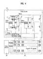
- FIG.4 illustrates an organic EL display panel and operation module thereof (more specifically, a data driver) according to the present invention.
- the data driver 10 for the organic EL display includes a current reference generator 11 for providing a drive current for use in a display panel 30 in PAM mode, an analog Mux 12 for switching a data drive current reference from the current reference generator 11 with a charge/discharge current reference being inputted, a data driver output 13 for providing the current directly to the organic EL panel 30 according to the reference value, and a timing generator 14 for controlling data drive timing, charge timing and discharge timing.
- the above-described structure is designed in such a manner that the quantity of light emitted from the organic EL panel 30 is proportional to the amount of the current flowing in each pixel PE.
- the quality of light being generated can be controlled by controlling the amount of the current flowing in the pixels PE in the organic PE panel 30 in accordance with an input data in the current reference generator 11.
- the current reference generator 11 provides the drive current in PAM mode. Moreover, the current reference generator 11 not only generates a data drive current but also a charge/ discharge current reference according to the data difference between a previous scan line data and a next scan line data, whereby the discharge current that has no effective contribution towards the emission of light can be reduced.
- FIG.5 is a block diagram illustrating an internal structure of the current reference generator according to the present invention.
- the current reference generator 11 includes a memory 111 for saving an N-th scan line data, a memory 112 for saving an (N-1)-th scan line data, a subtracter 113 for obtaining a difference between the N-th and the (N-1)-th scan line data, a data latch 114 for saving the N-th scan line data and the result of the subtraction outputted from the subtracter 113, a D/A converter (Digital-Analog Converter) 115 for converting the N-th scan line data to an analog data and thereby generating a reference in need of the operation of the display panel, and a D/A converter2 116 for converting the result of the subtraction to an analog data and thereby generating a reference for charging or discharging according to the reference.
- a D/A converter Digital-Analog Converter
- An input data in the current reference generator 11 is saved in the N-th line data memory 111, and a previously inputted data is saved in the (N-1)-th line data memory 112.
- the D/A converter 1 115 generates a data drive current reference proportional to the N-th scan line data.
- the subtracter 113 finds the difference between the N-th scan line data and the (N-1)-th scan line data. If the N-th scan line data is greater, the D/A converter2 116 generates a charge current reference (i.e., current or voltage) in proportion to the difference.
- a charge current reference i.e., current or voltage
- the D/A converter2 116 generates a discharge current reference (i.e., current or voltage) in proportion to the difference.
- the data drive current reference, charge current reference or discharge current reference, and a timing value for each of the reference current values generated from the timing generator 14 get muxed through the analog Mux 12 and are outputted to the data driver output 13.
- a voltage enters the data driver output 13 via a VDDA line and an appropriate current for the current reference value is supplied directly to the organic EL panel. In this manner, the organic EL panel 30 is able to emit light.
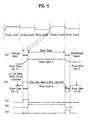
- the output waveform of the data driver output 13 is illustrated in FIG.6.
- the output waveform of the data driver output 13 is explained in more detail as follows.
- FIG.6(a) illustrates part of the output waveform of the data driver output according to the present invention. Particularly, the drawing depicts a change in the voltage.
- the voltage change is proportional to the difference between the (N-1)-th scan line and the N-th scan line. This explains why the voltage waveform reflects a linear shape at the transition of line driving.
- FIG.6(b) illustrates part of the output waveform of the data driver output according to the present invention. Particularly, the drawing depicts a change in the current.
- the drive current in the N-th scan line is higher than the drive current in the (N-1)-th scan line.
- a current for balancing the difference should be charged.
- the charge or discharge current is slightly higher than the change of the amplitude of the data drive current in order to reduce the charging or discharging period of time.
- FIG.6(c) to FIG.6(e) illustrate, respectively, the timing of the current generation corresponding to part of the output waveform of the data driver output according to the present invention.
- the drive current in the N-th scan line is higher than the drive current in the (N-1)-th scan line, so a current for balancing the difference is charged at the timing given in FIG.6(c).
- FIG.6(d) illustrates a data drive timing for generating a drive current for the data that corresponds to the N-th scan line.
- FIG.6(e) illustrates a discharge timing.
- the drive current in the (N-1)-th scan line is lower than the drive current in the N-th scan line, so a current for balancing the difference is discharged at the timing given in FIG.6(e).
- the amplitude of the charge and the discharge current can be fixed, and the optimal charge and discharge time proportional to the data difference between the scan lines can be obtained by properly controlling the timing(s) of the timing generator, thereby regulating the amount of the charge and discharge current.
- the present invention can also be applied to other flat panel displays in PAM mode, including LCDs, FEDs, and PDPs.
- the apparatus and method for operating the organic EL display panel according to the present invention has the following advantages.
- the organic EL display panel can be operated with low power consumption without deteriorations in the picture quality.
Landscapes
- Engineering & Computer Science (AREA)
- Physics & Mathematics (AREA)
- Computer Hardware Design (AREA)
- General Physics & Mathematics (AREA)
- Theoretical Computer Science (AREA)
- Water Supply & Treatment (AREA)
- Control Of Indicators Other Than Cathode Ray Tubes (AREA)
- Electroluminescent Light Sources (AREA)
- Control Of El Displays (AREA)
Abstract
Description
- This application claims the benefit of the Korean Patent Application No. 10-2004-0001802, filed on January 10, 2004, which is hereby incorporated by reference as if fully set forth herein.
- The present invention relates in general to a flat panel display, and more particularly, to an apparatus and method for operating a flat panel display.
- Technical advances in cathode ray tubes have brought the development of flat panel displays with reduced weight and volume. Examples of the flat panel display include LCDs (Liquid Crystal Displays), FEDs (Field Emission Displays), PDPs (Plasma Display Panels), and organic EL (Electro Luminescence)displays.
- Particularly, the organic EL display stands along among other LCDs for its many advantages including a thinner screen, faster response speed, superior visibility due to the self-luminescent characteristics, and larger viewing angle. Thus, many studies are now under way in worldwide.
- Organic EL displays come in diverse operation systems depending on their size. For instance, a large and medium-sized organic EL display adopts an active operating system, and a small-sized organic EL display adopts both active and passive operating systems.
- More specifically, the passive operating system for the small-sized organic EL display utilizes pulse width modulation (hereinafter it is referred to as ' PWM' ) and pulse amplitude modulation (hereinafter it is referred to as ' PAM').
- To explain how the organic EL display is operated, FIG.1 illustrates a related art organic EL display panel and operation module thereof.
- As shown in FIG.1, the operation module of the organic EL display panel includes an organic
EL display panel 3, adata driver 1 for operating thepanel 3, and ascan driver 2. - If an enable signal is issued sequentially to each line through the
scan driver 2 thedata driver 1 provides a data signal through a data line, and each pixel PE of the organicEL display panel 3 generates light corresponding to the magnitude of the data signal. - In effect, the PWM and the PAM are distinguished by the output waveform of the data signals provided by the
data driver 1. More details on these will be provided with reference to drawings. - FIG.2 illustrates an output waveform of a data driver when the organic EL display panel of FIG. 1 is in PWM mode.
- As shown in FIG.2, in PWM mode, the brightness of a screen is determined by the amplitude of a current provided by the data driver and the pulse width.
- That is, to exhibit a desired brightness in every scan line, discharging and charging take place for the adjustment of the pulse width.
- Although the amount of charge supplied is great, the discharge current is not sufficient enough to drive the pixels of the display panel for illumination. Therefore, power consumption in PWM mode was extremely high.
- FIG.3 illustrates an output waveform of a data driver when the organic EL display panel of FIG. 1 is in PAM mode.
- As shown in FIG.3, the brightness of a screen in PAM mode is inversely proportional to the amplitude of the driving current provided by the data driver.
- Similar to the PWM mode, the data driver output is discharged and charged per scan line.
- Even though the discharge current in the PAM mode is relatively less than that of the PWM mode, it is still not sufficient to drive the display panel for illumination. Therefore, the power consumption problem has remained unsolved.
- There have been many attempts to solve the above problem by not discharging the accumulated charge at the data driver output in the PAM mode for example. However in such case, the brightness of a next scan line was varied according to the amount of accumulated charge at the data driver output of the previous scan line, which in turn created deviated image brightness and deteriorated the picture quality.
- Accordingly, the present invention is directed to an apparatus and method for operating a flat panel display that substantially obviates one or more problems due to limitations and disadvantages of the related art.
- An object of the present invention is to provide an apparatus and method for operating a flat panel display featuring low-power consumption and superior picture quality, by minimizing the discharge current that has no effective contribution towards the operation of the flat panel display (i.e., an organic EL display) and the generation of light thereby and reducing brightness deviation between lines.
- Additional advantages, objects, and features of the invention will be set forth in part in the description which follows and in part will become apparent to those having ordinary skill in the art upon examination of the following or may be learned from practice of the invention. The objectives and other advantages of the invention may be realized and attained by the structure particularly pointed out in the written description and claims hereof as well as the appended drawings.
- To achieve these objects and other advantages and in accordance with the purpose of the invention, as embodied and broadly described herein, there is provided an apparatus for operating a flat panel display with a plurality of data lines and scan lines, in which the apparatus includes: a current reference generator for generating a data drive current reference for providing a drive current proportional to the size of an input data from outside, and a charge/discharge current reference according to a difference of the data size between the scan lines; and a data driver output for providing directly to the display panel a current corresponding to each of the current references.
- In the exemplary embodiment, the current reference generator compares among the scan lines a previous line data with a next line data to be driven, and generates the charge/discharge current reference according to the difference between the drive currents.
- In the exemplary embodiment, if the drive current of the previous line is higher than the drive current of the next line to be driven, the charge reference for balancing the difference current is generated. Also, if the drive current of the previous line is lower than the drive current of the next line to be driven, the discharge reference for balancing the difference current is generated.
- Preferably, the apparatus further includes: an analog Mux for muxing the drive current reference generated from the current reference generator, and the charge/discharge current reference being inputted.
- Preferably, the apparatus further includes: a timing generator for providing a timing for current supply according to each of the current references.
- In the exemplary embodiment, the current reference generator includes: a first memory for saving an N-th scan line data; a second memory for saving a previously inputted (N-1)-th line scan data; a subtracter for obtaining a difference between the N-th and the (N-1)-th scan line data; a first D/A converter (Digital-Analog Converter) for converting the N-th scan line data to an analog data and thereby, generating the drive current reference; and a second D/A converter for receiving the result of the subtraction outputted from the subtracter and thereby, generating the charge/discharge current reference according to the result.
- Another aspect of the present invention provides a method for operating a flat panel display with a plurality of data lines and scan lines, the method including the steps of: generating a data drive current reference for providing a drive current proportional to the size of an input data from outside; generating a charge/discharge current reference according to a difference of the data size between the scan lines; and providing directly to the display panel a current corresponding to each of the current references.
- In another aspect of the present invention, a method for operating a flat panel display with a plurality of data lines and scan lines includes the steps of: generating a charge/discharge current reference proportional to a difference of the data size between the scan lines; and adjusting a charge/discharge current supply timing according to the charge/discharge current reference, and outputting a corresponding current to the flat panel display.
- In the exemplary embodiment, the charge/discharge current reference is generated by comparing among the scan lines a previous line data with a next line data to be driven, and generating the charge/discharge current reference according to the difference between the drive currents.
- In the exemplary embodiment, the amplitude of the charge/discharge current is fixed at a predetermined level.
- It is to be understood that both the foregoing general description and the following detailed description of the present invention are exemplary and explanatory and are intended to provide further explanation of the invention as claimed.
- The accompanying drawings, which are included to provide a further understanding of the invention and are incorporated in and constitute a part of this application, illustrate embodiment(s) of the invention and together with the description serve to explain the principle of the invention. In the drawings:
- FIG.1 illustrates a related art organic EL display panel and operation module thereof;
- FIG.2 illustrates an output waveform of a data driver in PWM mode according to the related art;
- FIG.3 illustrates an output waveform of a data driver in PWM mode according to the related art;
- FIG.4 illustrates an organic EL display panel and operation module thereof according to the present invention;
- FIG.5 illustrates an internal structure of a current reference generator according to the present invention; and
- FIG.6 illustrates an output waveform of a data driver in PAM mode according to the present invention.
- Reference will now be made in detail to the preferred embodiments of the present invention, examples of which are illustrated in the accompanying drawings.
- The terminology used in the following description is general ones that are currently being used. There are also new terms introduced by the applicants of the present invention to describe a new technology in a best way. Those new terms will be explicitly explained in corresponding places. Therefore, it should be noted that the present invention is not to be understood simply by terminology itself but by the technical features and meanings associated with the terminology.
- FIG.4 illustrates an organic EL display panel and operation module thereof (more specifically, a data driver) according to the present invention.
- As shown in FIG.4, the
data driver 10 for the organic EL display includes acurrent reference generator 11 for providing a drive current for use in adisplay panel 30 in PAM mode, ananalog Mux 12 for switching a data drive current reference from thecurrent reference generator 11 with a charge/discharge current reference being inputted, adata driver output 13 for providing the current directly to theorganic EL panel 30 according to the reference value, and atiming generator 14 for controlling data drive timing, charge timing and discharge timing. - The above-described structure is designed in such a manner that the quantity of light emitted from the
organic EL panel 30 is proportional to the amount of the current flowing in each pixel PE. Thus, the quality of light being generated can be controlled by controlling the amount of the current flowing in the pixels PE in theorganic PE panel 30 in accordance with an input data in thecurrent reference generator 11. - Here, the
current reference generator 11 provides the drive current in PAM mode. Moreover, thecurrent reference generator 11 not only generates a data drive current but also a charge/ discharge current reference according to the data difference between a previous scan line data and a next scan line data, whereby the discharge current that has no effective contribution towards the emission of light can be reduced. - The following will now elaborate the operational procedure of the
current reference generator 11 with reference to FIG.5. - FIG.5 is a block diagram illustrating an internal structure of the current reference generator according to the present invention.
- As shown in FIG.5, the
current reference generator 11 includes amemory 111 for saving an N-th scan line data, amemory 112 for saving an (N-1)-th scan line data, asubtracter 113 for obtaining a difference between the N-th and the (N-1)-th scan line data, adata latch 114 for saving the N-th scan line data and the result of the subtraction outputted from thesubtracter 113, a D/A converter (Digital-Analog Converter) 115 for converting the N-th scan line data to an analog data and thereby generating a reference in need of the operation of the display panel, and a D/A converter2 116 for converting the result of the subtraction to an analog data and thereby generating a reference for charging or discharging according to the reference. - The operational relations between the elements in the
current reference generator 11 will now be explained below. - An input data in the
current reference generator 11 is saved in the N-thline data memory 111, and a previously inputted data is saved in the (N-1)-thline data memory 112. - The D/
A converter 1 115 generates a data drive current reference proportional to the N-th scan line data. - The
subtracter 113 finds the difference between the N-th scan line data and the (N-1)-th scan line data. If the N-th scan line data is greater, the D/A converter2 116 generates a charge current reference (i.e., current or voltage) in proportion to the difference. - On the other hand, if the N-th scan line data is smaller the D/A converter2 116 generates a discharge current reference (i.e., current or voltage) in proportion to the difference.
- Thusly generated data drive current reference, charge current reference or discharge current reference is inputted into the
analog Mux 12 of FIG.4. - The data drive current reference, charge current reference or discharge current reference, and a timing value for each of the reference current values generated from the
timing generator 14 get muxed through theanalog Mux 12 and are outputted to thedata driver output 13. - A voltage enters the
data driver output 13 via a VDDA line and an appropriate current for the current reference value is supplied directly to the organic EL panel. In this manner, theorganic EL panel 30 is able to emit light. - The output waveform of the
data driver output 13 is illustrated in FIG.6. - As illustrated in FIG.6, light is not emitted by performing the discharging and charging, and the output waveform of the
data driver output 13 is varied according to the difference between the present scan line and the previous scan line. - The output waveform of the
data driver output 13 is explained in more detail as follows. - FIG.6(a) illustrates part of the output waveform of the data driver output according to the present invention. Particularly, the drawing depicts a change in the voltage.
- Referring to FIG.6(a), the voltage change is proportional to the difference between the (N-1)-th scan line and the N-th scan line. This explains why the voltage waveform reflects a linear shape at the transition of line driving.
- In PAM mode, the deviation between the lines for the same data rarely exists because the charging and discharging time are much shorter than the data drive time.
- FIG.6(b) illustrates part of the output waveform of the data driver output according to the present invention. Particularly, the drawing depicts a change in the current.
- As illustrated in FIG.6(b), the drive current in the N-th scan line is higher than the drive current in the (N-1)-th scan line. Thus, a current for balancing the difference should be charged.
- Similarly, since the drive current in the (N+1)-th scan line is lower than the drive current in the N-th scan line, a current for balancing the difference should be discharged.
- At this time, the charge or discharge current is slightly higher than the change of the amplitude of the data drive current in order to reduce the charging or discharging period of time.
- FIG.6(c) to FIG.6(e) illustrate, respectively, the timing of the current generation corresponding to part of the output waveform of the data driver output according to the present invention.
- More specifically, in FIG.6(c), the drive current in the N-th scan line is higher than the drive current in the (N-1)-th scan line, so a current for balancing the difference is charged at the timing given in FIG.6(c).
- FIG.6(d) illustrates a data drive timing for generating a drive current for the data that corresponds to the N-th scan line.
- Lastly, FIG.6(e) illustrates a discharge timing. As is seen in the drawing, the drive current in the (N-1)-th scan line is lower than the drive current in the N-th scan line, so a current for balancing the difference is discharged at the timing given in FIG.6(e).
- Comparing the output waveform of the data driver output in FIG.6 with that of the related art in FIG.3, it is evident that the amount of the discharge current that has no effective contribution towards the emission of light is much reduced.
- Besides the above-described method, the amplitude of the charge and the discharge current can be fixed, and the optimal charge and discharge time proportional to the data difference between the scan lines can be obtained by properly controlling the timing(s) of the timing generator, thereby regulating the amount of the charge and discharge current.
- Meanwhile, the present invention can also be applied to other flat panel displays in PAM mode, including LCDs, FEDs, and PDPs.
- In conclusion, the apparatus and method for operating the organic EL display panel according to the present invention has the following advantages.
- Firstly, by regulating the amount of the charge and discharge current for data drive according to the size of the input data, the amount of the discharge current that has no effective contribution towards the emission of light was much reduced, which in turn reduced the total power consumption.
- Secondly, by reducing the brightness deviation between lines, the organic EL display panel can be operated with low power consumption without deteriorations in the picture quality.
- The forgoing embodiments are merely exemplary and are not to be construed as limiting the present invention. The present teachings can be readily applied to other types of apparatuses. The description of the present invention is intended to be illustrative, and not to limit the scope of the claims. Many alternatives, modifications, and variations will be apparent to those skilled in the art.
- The claims refer to examples of preferred embodiments of the invention. However, the invention also refers to the use of any single feature and subcombination of features which are disclosed in the claims, the description and / or the drawings.
Claims (17)
- An apparatus for operating a flat panel display with a plurality of data lines and scan lines, the apparatus comprising:a current reference generator for generating a data drive current reference for providing a drive current proportional to the size of an input data from outside, and a charge/discharge current reference according to a difference of the data size between the scan lines; anda data driver output for providing directly to the display panel a current corresponding to each of the current references.
- The apparatus according to claim 1, wherein the current reference generator compares among the scan lines a previous line data with a next line data to be driven, and generates the charge/discharge current reference according to the difference between the drive currents.
- The apparatus according to claim 2, wherein if the drive current of the previous line is higher than the drive current of the next line to be driven, the charge reference for balancing the difference current is generated.
- The apparatus according to claim 2, wherein if the drive current of the previous line is lower than the drive current of the next line to be driven, the discharge reference for balancing the difference current is generated.
- The apparatus according to claim 1, further comprising:an analog Mux for muxing the drive current reference generated from the current reference generator, and the charge/discharge current reference being inputted.
- The apparatus according to claim 1, further comprising:a timing generator for providing a timing for current supply according to each of the current references.
- The apparatus according to claim 1, wherein the current reference generator comprises:a first memory for saving an N-th scan line data;a second memory for saving a previously inputted (N-1)-th line scan data;a subtracter for obtaining a difference between the N-th and the (N-1)-th scan line data;a first D/A converter (Digital-Analog Converter) for converting the N-th scan line data to an analog data and thereby, generating the drive current reference; anda second D/A converter for receiving the result of the subtraction outputted from the subtracter and thereby, generating the charge/discharge current reference according to the result.
- A method for operating a flat panel display with a plurality of data lines and scan lines, the method comprising the steps of:generating a data drive current reference for providing a drive current proportional to the size of an input data from outside;generating a charge/discharge current reference according to a difference of the data size between the scan lines; andproviding directly to the display panel a current corresponding to each of the current references.
- The method according to claim 8, wherein the charge/discharge current reference is generated by comparing among the scan lines a previous line data with a next line data to be driven, and generating the charge/discharge current reference according to the difference between the drive currents.
- The method according to claim 9, wherein if the drive current of the previous line is higher than the drive current of the next line to be driven, the charge reference for balancing the difference current is generated.
- The method according to claim 9, wherein if the drive current of the previous line is lower than the drive current of the next line to be driven, the discharge reference for balancing the difference current is generated.
- The method according to claim 8, further comprising the step of:providing a timing for current supply according to each of the current references.
- The method according to claim 12, further comprising:switching (or muxing) one of the drive current, the charge current and the discharge current according to the timing given, and outputting a corresponding current.
- The method according to claim 8, wherein the charge/discharge current reference generating step comprises the sub-steps of:saving the N-th scan line data and the (N-1)-th line scan data, respectively;obtaining a difference between the N-th and the (N-1)-th scan line data;converting a current or voltage proportional to the difference into an analog data, and generating the charge or discharge current reference.
- A method for operating a flat panel display with a plurality of data lines and scan lines, the method comprising the steps of:generating a charge/discharge current reference proportional to a difference of the data size between the scan lines; andadjusting a charge/discharge current supply timing according to the charge/discharge current reference, and outputting a corresponding current to the flat panel display.
- The method according to claim 15, wherein the charge/discharge current reference is generated by comparing among the scan lines a previous line data with a next line data to be driven, and generating the charge/discharge current reference according to the difference between the drive currents.
- The method according to claim 15, wherein the amplitude of the charge/discharge current is fixed at a predetermined level.
Applications Claiming Priority (2)
| Application Number | Priority Date | Filing Date | Title |
|---|---|---|---|
| KR2004001802 | 2004-01-10 | ||
| KR1020040001802A KR100565664B1 (en) | 2004-01-10 | 2004-01-10 | Flat Panel Display Panel Driving Device and Method |
Publications (2)
| Publication Number | Publication Date |
|---|---|
| EP1553551A2 true EP1553551A2 (en) | 2005-07-13 |
| EP1553551A3 EP1553551A3 (en) | 2005-09-21 |
Family
ID=34588139
Family Applications (1)
| Application Number | Title | Priority Date | Filing Date |
|---|---|---|---|
| EP05000270A Withdrawn EP1553551A3 (en) | 2004-01-10 | 2005-01-07 | Apparatus and method for operating flat panel display |
Country Status (5)
| Country | Link |
|---|---|
| US (1) | US20050151707A1 (en) |
| EP (1) | EP1553551A3 (en) |
| JP (1) | JP2005196218A (en) |
| KR (1) | KR100565664B1 (en) |
| CN (1) | CN1637820A (en) |
Cited By (3)
| Publication number | Priority date | Publication date | Assignee | Title |
|---|---|---|---|---|
| EP1793365A2 (en) | 2005-11-30 | 2007-06-06 | LG Electronics Inc. | Light emitting device and method of driving the same |
| EP1850314A2 (en) | 2006-04-28 | 2007-10-31 | LG Electronics Inc. | Light emitting device and method of driving the same |
| WO2009011767A1 (en) | 2007-07-18 | 2009-01-22 | Eastman Kodak Company | Reduced power consumption in oled display system |
Families Citing this family (9)
| Publication number | Priority date | Publication date | Assignee | Title |
|---|---|---|---|---|
| US7714811B2 (en) * | 2005-09-12 | 2010-05-11 | Lg Electronics Inc. | Light-emitting device and method of driving the same |
| US7791567B2 (en) * | 2005-09-15 | 2010-09-07 | Lg Display Co., Ltd. | Organic electroluminescent device and driving method thereof |
| TWI348675B (en) * | 2006-04-07 | 2011-09-11 | Himax Tech Ltd | Method for driving display |
| KR100843690B1 (en) | 2006-04-24 | 2008-07-04 | 엘지디스플레이 주식회사 | Light emitting element |
| KR100736574B1 (en) * | 2006-04-28 | 2007-07-06 | 엘지전자 주식회사 | Light emitting device and method for driving same |
| TWI363330B (en) * | 2007-05-24 | 2012-05-01 | Au Optronics Corp | Pulse generation circuit and display apparatus for adjusting display brightness of a picture |
| CN108652564B (en) * | 2018-05-14 | 2022-03-11 | 佛山市顺德区美的洗涤电器制造有限公司 | Automatic wake-up method and device for dish washer and computer readable storage medium |
| JP7367006B2 (en) * | 2019-04-12 | 2023-10-23 | ラピスセミコンダクタ株式会社 | Display driver and display device |
| CN112863427B (en) * | 2021-01-13 | 2022-05-13 | 厦门天马微电子有限公司 | Method for adjusting brightness of light-emitting panel, light-emitting panel and display device |
Citations (1)
| Publication number | Priority date | Publication date | Assignee | Title |
|---|---|---|---|---|
| WO2005057545A1 (en) * | 2003-12-08 | 2005-06-23 | Koninklijke Philips Electronics N.V. | Display device driving circuit |
Family Cites Families (13)
| Publication number | Priority date | Publication date | Assignee | Title |
|---|---|---|---|---|
| US5910792A (en) * | 1997-11-12 | 1999-06-08 | Candescent Technologies, Corp. | Method and apparatus for brightness control in a field emission display |
| US6191534B1 (en) * | 1999-07-21 | 2001-02-20 | Infineon Technologies North America Corp. | Low current drive of light emitting devices |
| JP3341735B2 (en) * | 1999-10-05 | 2002-11-05 | 日本電気株式会社 | Driving device for organic thin film EL display device and driving method thereof |
| US6414661B1 (en) * | 2000-02-22 | 2002-07-02 | Sarnoff Corporation | Method and apparatus for calibrating display devices and automatically compensating for loss in their efficiency over time |
| JP3485175B2 (en) * | 2000-08-10 | 2004-01-13 | 日本電気株式会社 | Electroluminescent display |
| KR100370286B1 (en) * | 2000-12-29 | 2003-01-29 | 삼성에스디아이 주식회사 | circuit of electroluminescent display pixel for voltage driving |
| US6667580B2 (en) * | 2001-07-06 | 2003-12-23 | Lg Electronics Inc. | Circuit and method for driving display of current driven type |
| US20030058196A1 (en) * | 2001-09-26 | 2003-03-27 | Hansen Ronald L. | Method for reducing power consumption in field emission display devices by efficiently controlling column driver output voltage |
| US20030169241A1 (en) * | 2001-10-19 | 2003-09-11 | Lechevalier Robert E. | Method and system for ramp control of precharge voltage |
| US20030117382A1 (en) * | 2001-12-07 | 2003-06-26 | Pawlowski Stephen S. | Configurable panel controller and flexible display interface |
| JP3995505B2 (en) * | 2002-03-25 | 2007-10-24 | 三洋電機株式会社 | Display method and display device |
| TW591575B (en) * | 2002-05-28 | 2004-06-11 | Au Optronics Corp | Driving circuit of liquid crystal display panel and method thereof, and liquid crystal display |
| KR100903099B1 (en) * | 2003-04-15 | 2009-06-16 | 삼성모바일디스플레이주식회사 | Method and device for driving an electroluminescent display panel that efficiently performs booting |
-
2004
- 2004-01-10 KR KR1020040001802A patent/KR100565664B1/en not_active Expired - Fee Related
-
2005
- 2005-01-07 US US11/030,195 patent/US20050151707A1/en not_active Abandoned
- 2005-01-07 EP EP05000270A patent/EP1553551A3/en not_active Withdrawn
- 2005-01-10 CN CNA2005100003621A patent/CN1637820A/en active Pending
- 2005-01-11 JP JP2005004086A patent/JP2005196218A/en active Pending
Patent Citations (1)
| Publication number | Priority date | Publication date | Assignee | Title |
|---|---|---|---|---|
| WO2005057545A1 (en) * | 2003-12-08 | 2005-06-23 | Koninklijke Philips Electronics N.V. | Display device driving circuit |
Cited By (8)
| Publication number | Priority date | Publication date | Assignee | Title |
|---|---|---|---|---|
| EP1793365A2 (en) | 2005-11-30 | 2007-06-06 | LG Electronics Inc. | Light emitting device and method of driving the same |
| EP1793365A3 (en) * | 2005-11-30 | 2008-05-07 | LG Electronics Inc. | Light emitting device and method of driving the same |
| EP1850314A2 (en) | 2006-04-28 | 2007-10-31 | LG Electronics Inc. | Light emitting device and method of driving the same |
| EP1850314A3 (en) * | 2006-04-28 | 2009-12-16 | LG Display Co., Ltd. | Light emitting device and method of driving the same |
| US7898508B2 (en) | 2006-04-28 | 2011-03-01 | Lg Display Co., Ltd. | Light emitting device and method of driving the same |
| US8416160B2 (en) | 2006-04-28 | 2013-04-09 | Lg Display Co., Ltd. | Light emitting device and method of driving the same |
| WO2009011767A1 (en) | 2007-07-18 | 2009-01-22 | Eastman Kodak Company | Reduced power consumption in oled display system |
| US8269798B2 (en) | 2007-07-18 | 2012-09-18 | Global Oled Technology Llc | Reduced power consumption in OLED display system |
Also Published As
| Publication number | Publication date |
|---|---|
| KR20050073737A (en) | 2005-07-18 |
| EP1553551A3 (en) | 2005-09-21 |
| KR100565664B1 (en) | 2006-03-29 |
| US20050151707A1 (en) | 2005-07-14 |
| JP2005196218A (en) | 2005-07-21 |
| CN1637820A (en) | 2005-07-13 |
Similar Documents
| Publication | Publication Date | Title |
|---|---|---|
| KR100934597B1 (en) | Backlight Luminance Control for Liquid Crystal Display Panels | |
| US9542883B2 (en) | Device and method for controlling brightness of organic light emitting diode display | |
| JP5241154B2 (en) | Organic light emitting diode display device and driving method thereof | |
| JP3404357B2 (en) | Apparatus and method for controlling brightness of flat display device | |
| US20080062089A1 (en) | Organic electro luminescence display device and driving method for the same | |
| US20070211011A1 (en) | Flat panel display device and data signal generating method thereof | |
| US8330684B2 (en) | Organic light emitting display and its driving method | |
| US20080204397A1 (en) | Backlight device and liquid crystal display device having the same | |
| US8581897B2 (en) | DC-DC converter and organic light emitting display using the same | |
| EP1553551A2 (en) | Apparatus and method for operating flat panel display | |
| KR102797685B1 (en) | Display device | |
| JP2005346076A (en) | Organic electroluminescent display device and driving method thereof | |
| CN112652267A (en) | Rolling screen display digital driving method for active Micro-LED display screen | |
| CN100524417C (en) | Organic electro-luminescent display device and method for driving the same | |
| US6960889B2 (en) | Method and apparatus for driving electro-luminescence display device | |
| EP1895495B1 (en) | Organic electroluminescent display device and driving method for the same | |
| KR101310912B1 (en) | OLED display and drive method thereof | |
| KR101310376B1 (en) | Organic Light Emitting Diode Display And Driving Method Thereof | |
| KR100400743B1 (en) | power saving circuit in display element of current driving type | |
| US7129915B2 (en) | Method and apparatus for driving electro-luminescence display device | |
| KR100421873B1 (en) | Analog driving circuit in display element | |
| KR100620992B1 (en) | Flat Panel Display Panel Driving Device and Method | |
| US8988323B2 (en) | Organic light emitting display and control signal generating circuit of organic light emitting display | |
| KR100433215B1 (en) | Electro luminescence panel and driving apparatus and method thereof | |
| KR100492542B1 (en) | Apparatus for driving flat display device |
Legal Events
| Date | Code | Title | Description |
|---|---|---|---|
| PUAI | Public reference made under article 153(3) epc to a published international application that has entered the european phase |
Free format text: ORIGINAL CODE: 0009012 |
|
| 17P | Request for examination filed |
Effective date: 20050110 |
|
| AK | Designated contracting states |
Kind code of ref document: A2 Designated state(s): AT BE BG CH CY CZ DE DK EE ES FI FR GB GR HU IE IS IT LI LT LU MC NL PL PT RO SE SI SK TR |
|
| AX | Request for extension of the european patent |
Extension state: AL BA HR LV MK YU |
|
| PUAL | Search report despatched |
Free format text: ORIGINAL CODE: 0009013 |
|
| AK | Designated contracting states |
Kind code of ref document: A3 Designated state(s): AT BE BG CH CY CZ DE DK EE ES FI FR GB GR HU IE IS IT LI LT LU MC NL PL PT RO SE SI SK TR |
|
| AX | Request for extension of the european patent |
Extension state: AL BA HR LV MK YU |
|
| AKX | Designation fees paid |
Designated state(s): DE FR GB NL |
|
| STAA | Information on the status of an ep patent application or granted ep patent |
Free format text: STATUS: THE APPLICATION HAS BEEN WITHDRAWN |
|
| 18W | Application withdrawn |
Effective date: 20120126 |