EP1551042B1 - High voltage capacitor for magnetron - Google Patents
High voltage capacitor for magnetron Download PDFInfo
- Publication number
- EP1551042B1 EP1551042B1 EP04026584A EP04026584A EP1551042B1 EP 1551042 B1 EP1551042 B1 EP 1551042B1 EP 04026584 A EP04026584 A EP 04026584A EP 04026584 A EP04026584 A EP 04026584A EP 1551042 B1 EP1551042 B1 EP 1551042B1
- Authority
- EP
- European Patent Office
- Prior art keywords
- high voltage
- voltage capacitor
- insulating
- central conductors
- dielectric ceramics
- Prior art date
- Legal status (The legal status is an assumption and is not a legal conclusion. Google has not performed a legal analysis and makes no representation as to the accuracy of the status listed.)
- Expired - Lifetime
Links
- 239000003990 capacitor Substances 0.000 title claims description 84
- 239000000919 ceramic Substances 0.000 claims description 70
- 239000004020 conductor Substances 0.000 claims description 66
- 239000002184 metal Substances 0.000 claims description 58
- 239000000945 filler Substances 0.000 claims description 32
- 239000006096 absorbing agent Substances 0.000 claims description 30
- 238000000926 separation method Methods 0.000 description 5
- 239000007788 liquid Substances 0.000 description 4
- 229910000859 α-Fe Inorganic materials 0.000 description 4
- 238000001816 cooling Methods 0.000 description 3
- 238000001914 filtration Methods 0.000 description 2
- 239000000463 material Substances 0.000 description 2
- 238000000034 method Methods 0.000 description 2
- 238000003466 welding Methods 0.000 description 2
- 238000007792 addition Methods 0.000 description 1
- 230000015556 catabolic process Effects 0.000 description 1
- 239000013013 elastic material Substances 0.000 description 1
- 239000003822 epoxy resin Substances 0.000 description 1
- 238000004299 exfoliation Methods 0.000 description 1
- 238000004519 manufacturing process Methods 0.000 description 1
- 238000012986 modification Methods 0.000 description 1
- 230000004048 modification Effects 0.000 description 1
- 229920000647 polyepoxide Polymers 0.000 description 1
- 230000005855 radiation Effects 0.000 description 1
- 229910052710 silicon Inorganic materials 0.000 description 1
- 239000010703 silicon Substances 0.000 description 1
- 238000005476 soldering Methods 0.000 description 1
- 238000006467 substitution reaction Methods 0.000 description 1
- 229920003002 synthetic resin Polymers 0.000 description 1
- 239000000057 synthetic resin Substances 0.000 description 1
- 239000010409 thin film Substances 0.000 description 1
Images





Classifications
-
- H—ELECTRICITY
- H01—ELECTRIC ELEMENTS
- H01J—ELECTRIC DISCHARGE TUBES OR DISCHARGE LAMPS
- H01J23/00—Details of transit-time tubes of the types covered by group H01J25/00
- H01J23/16—Circuit elements, having distributed capacitance and inductance, structurally associated with the tube and interacting with the discharge
-
- H—ELECTRICITY
- H01—ELECTRIC ELEMENTS
- H01G—CAPACITORS; CAPACITORS, RECTIFIERS, DETECTORS, SWITCHING DEVICES, LIGHT-SENSITIVE OR TEMPERATURE-SENSITIVE DEVICES OF THE ELECTROLYTIC TYPE
- H01G4/00—Fixed capacitors; Processes of their manufacture
- H01G4/35—Feed-through capacitors or anti-noise capacitors
Definitions
- the present invention relates to a high voltage capacitor for a magnetron, and more particularly to a high voltage capacitor for a magnetron, in which a dielectric ceramic is divided into a plurality of portions having an arch shape and electrodes are formed on the side surfaces of the plural portions of the dielectric ceramic.
- magnetrons are apparatuses for generating and outputting microwaves, installed in a microwave oven or etc., and include a high voltage condenser for inputting high voltage therethrough.
- US-A- 4 814 938 describes a high voltage capacitor for a magnetron.
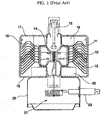
- Fig. 1 is a cross-sectional view of a conventional magnetron.
- the conventional magnetron comprises an anode unit including vanes 12 and straps 13 forming a resonance circuit when anode voltage and anode current having constant quantities are applied to the magnetron, a cathode unit 14 placed inside the anode unit for generating a large quantity of thermal electrons and generating microwaves in a space where the cathode unit 14 acts with ends of the vanes 12, an antenna 15 for transmitting the microwaves generated in the acting space to the outside, a plurality of cooling pins 16 installed on the outer periphery of the anode unit for radiating heat converted from residual energy, which is not transformed into the microwaves, yokes 17 and 18 for protecting and supporting the anode unit and the cooling pins 16 and guiding external air to the cooling pins 16, upper and lower permanent magnets 19 and 20 respectively placed on lower and upper surfaces of the yokes 17 and 18 for constituting a closed magnetic circuit, and a filter box 22 including an
- the anode unit includes an anode main body 11 having a cylindrical shape, a plurality of the vanes 12 installed in the anode main body 11, and the straps 13 passing through the vanes 12 for constituting the resonance circuit between the vanes 12 and the straps 13.
- the filter box 22 includes coils and ferrites for providing inductance to the LC filter 21, and a high pressure condenser 23 for inputting high voltage to the magnetron and providing capacitance to the LC filter 21 is installed on one side surface of the filter box 22.
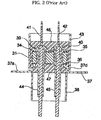
- Fig. 2 is a cross-sectional view of a conventional high voltage condenser for a magnetron
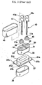
- Fig. 3 is an exploded perspective view of the conventional high voltage condenser.
- the conventional high voltage condenser 23 comprises a dielectric ceramic 31, a ground metal 37, a lower cover 38, metal caps 39 and 40, central conductors 41 and 42, an upper cover 43, insulating tubes 44 and 45, and insulating fillers 46 and 47.
- a pair of through holes 32 and 33 are formed through the dielectric ceramic 31, a pair of separation electrodes 34 and 35 are installed on the upper surface of the dielectric ceramic 31, and a common electrode 36 is installed on the lower surface of the dielectric ceramic 31.
- a plurality of connection holes 37b for fixing the ground metal 37 to the filter box 22 are formed through four corners of a plate unit 37a having a rectangular shape of the ground metal 37.
- a protuberance 37d connected to the common electrode 36 is formed on the center of the plate unit 37a, and a through hole 37c having an oval shape is formed through the protuberance 37d of the plate unit 37a.
- the metal caps 39 and 40 are bonded to the central conductors 41 and 42 and connected to the separation electrodes 34 and 35 so that the central conductors 41 and 42 and the separation electrodes 34 and 35 are connected.
- Taps 41a and 42b are respectively formed integrally with the upper ends of the central conductors 41 and 42, and the central conductors 41 and 42 sequentially pass through the metal caps 39 and 40, the through holes 32 and 33 of the dielectric ceramic 31, and the oval through holes 37c of the ground metal 37, and are soldered to the metal caps 39 and 40.
- the central conductors 41 and 42 are covered with the insulating tubes 44 and 45 made of a material having elasticity, such as silicon.
- the insulating fillers 46 and 47 are closer to the central conductors 41 and 42 than to the dielectric ceramic 31.
- the insulating fillers 46 and 47 are exfoliated from the dielectric ceramic 31 due to residual stress of the insulating fillers 46 and 47 or stress generated by the variation in temperature, thereby depreciating withstand voltage.
- the insulating tubes 44 and 45 made of an elastic material, which coat the central conductors 41 and 42, prevent the above depreciation of the withstand voltage.
- the lower cover 38 is attached to the ground metal 37, thereby surrounding the lower parts of the central conductors 41 and 42 coated with the insulating tubes 44 and 45.
- the upper cover 43 is attached to the ground metal 37, thereby surrounding the dielectric ceramic 31, the metal caps 39 and 40, and the upper parts of the central conductors 41 and 42.
- the high voltage condenser 23 is installed such that the inside of the high pressure condenser 23 is vertically divided by the ground metal 37, the dielectric ceramic 31 and the metal caps 39 and 40.
- the insulating fillers 46 and 47 are respectively injected into the high voltage condenser 23 through an opening of the upper cover 43 and an opening of the lower cover 38.
- the insulating filler 46 which is injected into the high voltage condenser 23 through the opening of the upper cover 43, surrounds the outer surfaces of the dielectric ceramic 31 and the metal caps 39 and 40 and the upper parts of the central conductors 41 and 42
- the insulating filler 47 which is injected into the high voltage condenser 23 through the opening of the lower cover 38, fills the insides of the dielectric ceramic 31 and the metal caps 39 and 40 and surrounds the insulating tubes 44 and 45.
- the conventional high pressure condenser 23 Since the inside of the high voltage condenser 23 is vertically divided so that the insulating fillers 46 and 47 are injected into the high voltage condenser 23 by two steps, and is hardened, the conventional high pressure condenser 23 is disadvantageous in that time and costs taken to fill the high voltage condenser 23 with the insulating fillers 46 and 47 are increased, a step for soldering the metal caps 39 and 40 for connecting the central conductors 41 and 42 and the separation electrodes 34 and 35 is required, the central conductors 41 and 42 have complicated structures due to the attachment between the central conductors 41 and 42 and the metal caps 39 and 40, and the dielectric ceramic 31 and the insulating fillers 46 and 47 are interposed between the central conductors 41 and 42.
- the present invention has been made in view of the above problems, and it is an object of the present invention to provide a high voltage capacitor for a magnetron, in which a dielectric ceramic is divided into a plurality of portions having an arch shape and electrodes are formed on the side surfaces of the plural portions of the dielectric ceramic, thereby having a simple structure, simplifying an assembly process, and reducing production costs.
- a high voltage capacitor for a magnetron comprising: dielectric ceramics having an arch shape; internal electrodes respectively disposed along internal peripheries of the dielectric ceramics; central conductors respectively connected to the internal electrodes; external electrodes respectively disposed along external peripheries of the dielectric ceramics; a ground metal contacting the external electrodes; and an insulating filler surrounding the dielectric ceramics and the central conductors.
- a high voltage capacitor for a magnetron comprising: a pair of dielectric ceramics having an arch shape, and respectively including external electrodes disposed along external peripheries thereof and internal electrodes disposed along internal peripheries thereof; a pair of central conductors respectively connected to the internal electrodes; a ground metal including a tub unit contacting the external electrodes; an insulating case surrounding the dielectric ceramics and the tub unit; an insulating base inserted into the tub unit, and including a pair of through holes for passing the central conductors and a hollow protrusion disposed between a pair of the dielectric ceramics; and an insulating filler injected into the insulating case and hardened.
- a high voltage capacitor for a magnetron comprising: a pair of dielectric ceramics having an arch shape, and respectively including external electrodes disposed along external peripheries thereof and internal electrodes disposed along internal peripheries thereof; a pair of central conductors respectively connected to the internal electrodes; a ground metal including a tub unit contacting the external electrodes; an insulating case surrounding the dielectric ceramics and the tub unit; an insulating base inserted into the tub unit, and including a pair of through holes for passing the central conductors; an insulating filler injected into the insulating case and hardened; and an electromagnetic wave interruption gasket installed on the ground metal, and including a pair of second through holes for respectively passing the central conductors.
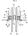
- Fig. 4 is a longitudinal-sectional view of a high voltage capacitor for a magnetron in accordance with a first embodiment of the present invention.
- Fig. 5 is a cross-sectional view of the high voltage capacitor in accordance with the first embodiment of the present invention.
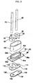
- Fig. 6 is an exploded perspective view of the high voltage capacitor in accordance with the first embodiment of the present invention.
- the high voltage capacitor in accordance with the first embodiment comprises two dielectric ceramics 50 and 60 having an arch shape, external electrodes 52 and 62 respectively disposed along the outer peripheries of the dielectric ceramics 50 and 60, and internal electrodes 54 and 64 respectively disposed along the inner peripheries of the dielectric ceramics 50 and 60.
- the external electrodes 52 and 62 and the internal electrodes 54 and 64 have an arch shape with a small thickness.
- a pair of the dielectric ceramics 50 and 60 are separated from each other such that the dielectric ceramics 50 and 60 are opposite to the internal electrodes 54 and 64.
- the above high voltage capacitor further comprises a pair of central conductors 70 and 80 respectively connected to the internal electrodes 54 and 64.
- the central conductors 70 and 80 contact the internal electrodes 54 and 64 by 180° of the whole peripheries thereof, and are welded to the internal electrodes 54 and 64.
- the central conductors 70 and 80 does not contact the whole peripheries (360°) of the internal electrodes 54 and 64, but rather contact the portions (180°) of the peripheries of the internal electrodes 54 and 64, stress between the central conductors 70 and 80 and the dielectric ceramics 50 and 60 is not generated when the high pressure condenser is turned on/off, the dielectric ceramics 50 and 60 are not exfoliated from an insulating filler 120, which will be described later, and an additional insulating tube for preventing the above exfoliation is not required.
- the high voltage capacitor further comprises a ground metal 92 connected to a filter box 22 of the magnetron by locking bolts 90.
- the ground metal 92 includes a tub unit 94 contacting the external electrodes 52 and 62, and a plate unit 96 protruded from the tub unit 94 outwardly.
- the tub unit 94 includes first and second rectilinear portions 94a and 94b, which are separated from each other so that they are opposite to each other, and first and second curved portions 94c and 94d, which have an arch shape equal to the shape of the dielectric ceramics 50 and 52, and is longitudinally hollowed.
- the tub unit 94 is welded to the external electrodes 52 and 62.
- the plate unit 96 is protruded from the end of the tub unit 94 outwardly, and connection holes 96a, into which the locking bolts 90 are respectively inserted, are formed through four corners of the plate unit 96.
- the high pressure condenser further comprises an insulating case 100 surrounding the dielectric ceramics 50 and 52 and the tub unit 94.
- the insulating case 100 has the same shape as that of the tub unit 94, so that the tub unit 94 is inserted into the insulating case 100, and a length larger than that of the tub unit 94, and is longitudinally hollowed.
- the high voltage capacitor further comprises an insulating base 116, which is inserted into the tub unit 94 and has a pair of through holes 112 and 114 for passing a pair of the central conductors 70 and 80.
- the insulating base 116 serves to close one opening of each of the insulating case 100 and the tub unit 94, and the external edge of the insulating base 116 has the same shape as that of the internal periphery of the tub unit 94.
- a hollow protrusion 118 is formed on the central portion of the insulating base 116 such that the protrusion 118 is located between the dielectric ceramics 50 and 60 and between the central conductors 70 and 80.
- the hollow protrusion 118 has a rectangular parallelepiped structure having a hollow therein and one opened surface.
- the insulating filler 120 together with the tub unit 94 and the insulating base 116 surrounds the dielectric ceramics 50 and 60 and parts of the central conductors 70 and 80 so as to have a sufficient withstand voltage, and is made of synthetic resin, such as epoxy resin.
- the insulating filler 120 is injected into the insulating case 100 through the other opening of the insulating case 100, is obstructed by the tub unit 94 and the insulating base 116, and is then hardened.
- the internal electrodes 54 and 64 of the dielectric ceramics 50 and 60 respectively contact the central conductors 70 and 80.
- the internal electrodes 54 and 64 are welded to the central conductors 70 and 80.
- the external electrodes 52 and 62 of the dielectric ceramics 50 and 60 respectively contact the inner periphery of the tub unit 94 of the ground metal 92, the external electrodes 52 and 62 are welded to the tub unit 94 of the ground metal 92.
- the dielectric ceramics 50 and 60 are separated from each other by a designated interval, thereby reducing the costs for a material needed in proportion to the above interval.
- the protrusion 118 of the insulating base 116 is inserted into the tub unit 94 of the ground metal 92 such that the protrusion 118 of the insulating base 116 is located between the dielectric ceramics 50 and 60. Then, openings of the tub unit 94 of the ground metal 92 and the insulating case 100 are closed by the insulating base 116, and the insides of the tub unit 94 of the ground metal 92 and the insulating case 100 are respectively divided into two spaces, i.e., left and right spaces, by the protrusion 118.
- the insulating filler 120 in a liquid state is injected into the insulating case 100 through the other opening of the insulating case 100.
- the injected liquid insulating filler 120 fills a space between the insulating case 100 and the external electrodes 52 and 62, and a space among the central conductors 70 and 80, the dielectric ceramics 50 and 60 and the protrusion 118.
- the injected liquid insulating filler 120 cannot fill the central portion of the insulating case 100, on which the protrusion 118 is formed.
- the liquid insulating filler 120 injected into the insulating case 100 is hardened, and surrounds the tub unit 94 of the ground metal 92, the insulating base 116, parts of the central conductors 70 and 80, and the dielectric ceramics 50 and 60.
- ground metal 92 is fixed to the filter box 22 by the locking bolts 90. Thereby, the assembly of the high voltage capacitor of the present invention is completed.
- the dielectric ceramics 50 and 60 of the above-assembled high voltage capacitor for the magnetron have a designated capacitance due to the phase difference between the external electrodes 52 and 62 and the internal electrodes 54 and 64, and filters out noise having passed through the high voltage capacitor.
- Fig. 7 is a cross-sectional view of a high voltage capacitor for a magnetron in accordance with a second embodiment of the present invention.
- Fig. 8 is an exploded perspective view of the high voltage capacitor in accordance with the second embodiment of the present invention.
- the high voltage capacitor in accordance with the second embodiment comprises a pair of the dielectric ceramics 50 and 60, a pair of the central conductors 70 and 80, the ground metal 92, the insulating case 100, the insulating base 116, and the insulating filler 120, which are substantially the same as the high voltage capacitor in accordance with the first embodiment, and further comprises an electromagnetic wave interruption gasket 134, having second through holes 130 and 132 for passing the central conductors 70 and 80, installed on the ground metal 92.
- the electromagnetic wave interruption gasket 134 is made of a metal thin film, and has an external periphery having the same shape as that of the tub unit 94 and teeth 136 formed along the external periphery thereof such that the electromagnetic wave interruption gasket 134 is inserted into the tub unit 94 of the ground metal 92 by press fit.
- the high voltage capacitor in accordance with this embodiment filters out noise passing through the high voltage capacitor.
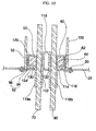
- Fig. 9 is a cross-sectional view of a high voltage capacitor for a magnetron in accordance with a third embodiment of the present invention.
- the high voltage capacitor in accordance with the third embodiment further comprises a pair of pipes 119a and 119b protruded integrally from the insulating base 116 respectively for passing the central conductors 70 and 80.
- Other parts of the high voltage capacitor in accordance with the third embodiment except for a pair of the pipes 119a and 119b are substantially the same as those of the high voltage capacitor in accordance with the first or second embodiment and are denoted by the same reference numerals even though they are depicted in different drawings, and a detailed description thereof will thus be omitted because it is considered to be unnecessary.
- the pipes 119a and 119b are connected to the through holes 112 and 114 of the insulating base 116 so that the pipes 119a and 119b surround the central conductors 70 and 80, and are integrally protruded from the insulating base 116 in the direction opposite to the protrusion 118.
- the high voltage capacitor in accordance with the third embodiment ensures an insulating distance.
- Fig. 10 is a cross-sectional view of a high voltage capacitor for a magnetron in accordance with a fourth embodiment of the present invention.
- the high voltage capacitor in accordance with the fourth embodiment further comprises a pair of the pipes 119a and 119b, protruded integrally from the insulating base 116 respectively for passing the central conductors 70 and 80, and an electromagnetic wave interruption gasket 134', having a pair of second through holes 130' and 132' for passing the central conductors 70 and 80 and the pipes 119a and 119b, installed on the ground metal 92.
- the high voltage capacitor in accordance with the fourth embodiment ensures an insulating distance, and high frequency waves are interrupted by the electromagnetic wave interruption gasket 134' when the magnetron is operated.
- Fig. 11 is a cross-sectional view of a high voltage capacitor for a magnetron in accordance with a fifth embodiment of the present invention.
- the high voltage capacitor in accordance with the fifth embodiment further comprises a high frequency absorber 140 installed on the ground metal 92 for passing a pair of the central conductors 70 and 80.
- Other parts of the high voltage capacitor in accordance with the fifth embodiment except for the high frequency absorber 140 are substantially the same as those of the high voltage capacitor in accordance with any one of the first to fourth embodiments and are denoted by the same reference numerals even though they are depicted in different drawings, and a detailed description thereof will thus be omitted because it is considered to be unnecessary.
- the high frequency absorber 140 is made of ferrite, and a pair of through holes 141 and 142 for passing the central conductors 70 and 80 are formed through the high frequency absorber 140.
- the external periphery of the high frequency absorber 140 has the same shape as that of the internal periphery of the tub unit 94 so that the high frequency absorber 140 is inserted into the tub unit 94 of the ground metal 92.
- the high frequency absorber 140 absorbs high frequency waves and the dielectric ceramics 50 and 60 have a designated capacitance when the magnetron is operated, the high voltage capacitor in accordance with the fifth embodiment filters out noise passing through the high frequency absorber.
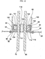
- Fig. 12 is a cross-sectional view of a high pressure voltage capacitor for a magnetron in accordance with a sixth embodiment of the present invention.
- the high voltage capacitor in accordance with the sixth embodiment further comprises a high frequency absorber 150 covering the insulating filler 120.
- Other parts of the high voltage capacitor in accordance with the sixth embodiment except for the high frequency absorber 150 are substantially the same as those of the high voltage capacitor in accordance with any one of the first to fourth embodiments and are denoted by the same reference numerals even though they are depicted in different drawings, and a detailed description thereof will thus be omitted because it is considered to be unnecessary.
- the high frequency absorber 150 is made of ferrite, and a pair of through holes 151 and 152 for passing the central conductors 70 and 80 are formed through the high frequency absorber 150.
- the external periphery of the high frequency absorber 150 has the same shape as that of the insulating case 100 so that the high frequency absorber 150 is inserted into the insulating case 100. After the insulating filler 120 is hardened, the high frequency absorber 150 is inserted into the insulating case 100.
- the protrusion 118 of the insulating base 116 may be covered with the high frequency absorber 150, or may pass through the high frequency absorber 150.
- non-described reference numeral 153 represents a through hole formed through the high frequency absorber 150 so that the protrusion 118 passes through the high frequency absorber 150.
- the dielectric ceramics 50 and 60 of the high voltage capacitor in accordance with the sixth embodiment have a designated capacitance when the magnetron is operated, thereby filtering out noise passing through the high voltage capacitor , and the high frequency absorber 150 absorbs high frequency waves.
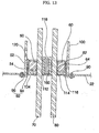
- Fig. 13 is a cross-sectional view of a high voltage capacitor for a magnetron in accordance with a seventh embodiment of the present invention.
- the high voltage capacitor in accordance with the seventh embodiment further comprises a high frequency absorber 160 installed inside the protrusion 118 of the insulating base 116.
- Other parts of the high voltage capacitor in accordance with the seventh embodiment except for the high frequency absorber 160 are substantially the same as those of the high voltage capacitor in accordance with any one of the first to fourth embodiments and are denoted by the same reference numerals even though they are depicted in different drawings, and a detailed description thereof will thus be omitted because it is considered to be unnecessary.
- the high frequency absorber 160 is made of ferrite, has the same shape as that of the inside of the hollow protrusion 118.
- the high frequency absorber 160 is inserted into the protrusion 118 through the opening of the protrusion 118.
- the dielectric ceramics 50 and 60 of the high voltage capacitor in accordance with the seventh embodiment have a designated capacitance when the magnetron is operated, thereby filtering out noise passing through the high voltage capacitor, and the high frequency absorber 160 absorbs high frequency waves having passed through the protrusion 118.
- Fig. 14 is a cross-sectional view of a high voltage capacitor for a magnetron in accordance with an eighth embodiment of the present invention.
- the high voltage capacitor in accordance with the eighth embodiment further comprises a tub 119c formed integrally with the insulating base 116 for protecting parts of the central conductors 70 and 80 having passed through the ground metal 92.
- Other parts of the high voltage capacitor in accordance with the eighth embodiment except for the tub 119c are substantially the same as those of the high voltage capacitor in accordance with any one of the first to fourth embodiments and are denoted by the same reference numerals even though they are depicted in different drawings, and a detailed description thereof will thus be omitted because it is considered to be unnecessary.
- the tub 119c has a designated length protruded from the base 116 in the direction opposite to the protrusion 118 such that the tub 119c is disposed around parts of the peripheries of the central conductors 70 and 80 having passed through the ground metal 92.
- the present invention provides a high voltage capacitor for a magnetron, in which a pair of dielectric ceramics having an arch shape are separated from each other, central conductors are connected to the internal peripheries of the dielectric ceramics, and a tub unit of a ground metal is connected to the external peripheries of the dielectric ceramics, thereby not requiring any additional structure for connecting the dielectric ceramics and the central conductors, simplifying the structures of the central conductors, and reducing the quantity of the dielectric ceramics needed in proportion to the separation interval between the dielectric ceramics.
- an insulating base including through holes for passing the central conductors is inserted into the tub unit of the ground metal, an insulating case surrounds the dielectric ceramics and the tub unit, and an insulating filler is injected into the insulating case, it is possible to inject the insulating filer into the insulating case and to harden the insulating filler by one step, thereby reducing working costs and time.
- a hollow protrusion is formed on the central portion of the insulating base between a pair of the dielectric ceramics, thereby reducing the quantity of the insulating filler needed in proportion to the dimensions of the protrusion.
- An electromagnetic wave interruption gasket is installed on the ground metal, thereby minimizing the outflow of electromagnetic waves through the high voltage capacitor.
- the central conductors and the internal electrodes of the dielectric ceramics are joined by welding and the tub unit of the ground metal and the external electrodes of the dielectric ceramics are joined by welding, thereby rapidly and simply achieving the joint therebetween.
- a pair of pipes for respectively passing the central conductors are protruded from the insulating base, thereby obtaining a sufficient insulating distance without any additional insulating tube.
- a tub for protecting parts of the central conductors passing through the ground metal is formed integrally with the insulating base, thereby preventing the breakdown of the central conductors.
- a high frequency absorber is installed on the ground metal or the protrusion of the insulating case or installed to cover the insulating filler, thereby minimizing the outflow of high frequency waves through the high.
- An electromagnetic wave interruption gasket is inserted into the tub unit of the ground metal by press fit through teeth formed along the external periphery thereof, thereby being easily installed on the ground metal of the high.
Landscapes
- Engineering & Computer Science (AREA)
- Power Engineering (AREA)
- Manufacturing & Machinery (AREA)
- Microelectronics & Electronic Packaging (AREA)
- Microwave Tubes (AREA)
- Fixed Capacitors And Capacitor Manufacturing Machines (AREA)
Description
- The present invention relates to a high voltage capacitor for a magnetron, and more particularly to a high voltage capacitor for a magnetron, in which a dielectric ceramic is divided into a plurality of portions having an arch shape and electrodes are formed on the side surfaces of the plural portions of the dielectric ceramic.
- Generally, magnetrons are apparatuses for generating and outputting microwaves, installed in a microwave oven or etc., and include a high voltage condenser for inputting high voltage therethrough.
- US-A- 4 814 938 describes a high voltage capacitor for a magnetron.
- Fig. 1 is a cross-sectional view of a conventional magnetron. The conventional magnetron comprises an anode
unit including vanes 12 andstraps 13 forming a resonance circuit when anode voltage and anode current having constant quantities are applied to the magnetron, acathode unit 14 placed inside the anode unit for generating a large quantity of thermal electrons and generating microwaves in a space where thecathode unit 14 acts with ends of thevanes 12, anantenna 15 for transmitting the microwaves generated in the acting space to the outside, a plurality ofcooling pins 16 installed on the outer periphery of the anode unit for radiating heat converted from residual energy, which is not transformed into the microwaves,yokes cooling pins 16 and guiding external air to thecooling pins 16, upper and lowerpermanent magnets yokes filter box 22 including anLC filter 21 for removing high-frequency radiation noise. - The anode unit includes an anode
main body 11 having a cylindrical shape, a plurality of thevanes 12 installed in the anodemain body 11, and thestraps 13 passing through thevanes 12 for constituting the resonance circuit between thevanes 12 and thestraps 13. - The
filter box 22 includes coils and ferrites for providing inductance to theLC filter 21, and ahigh pressure condenser 23 for inputting high voltage to the magnetron and providing capacitance to theLC filter 21 is installed on one side surface of thefilter box 22. - Fig. 2 is a cross-sectional view of a conventional high voltage condenser for a magnetron, and Fig. 3 is an exploded perspective view of the conventional high voltage condenser.
- As shown in Figs. 2 and 3, the conventional
high voltage condenser 23 comprises adielectric ceramic 31, aground metal 37, alower cover 38,metal caps central conductors upper cover 43,insulating tubes insulating fillers - A pair of through
holes separation electrodes common electrode 36 is installed on the lower surface of the dielectric ceramic 31. - A plurality of
connection holes 37b for fixing theground metal 37 to thefilter box 22 are formed through four corners of aplate unit 37a having a rectangular shape of theground metal 37. Aprotuberance 37d connected to thecommon electrode 36 is formed on the center of theplate unit 37a, and a throughhole 37c having an oval shape is formed through theprotuberance 37d of theplate unit 37a. - The
metal caps central conductors separation electrodes central conductors separation electrodes -
Taps 41a and 42b are respectively formed integrally with the upper ends of thecentral conductors central conductors metal caps holes holes 37c of theground metal 37, and are soldered to themetal caps - The
central conductors insulating tubes - The
insulating fillers central conductors insulating fillers insulating fillers insulating tubes central conductors - The
lower cover 38 is attached to theground metal 37, thereby surrounding the lower parts of thecentral conductors insulating tubes - The
upper cover 43 is attached to theground metal 37, thereby surrounding the dielectric ceramic 31, themetal caps central conductors - The
high voltage condenser 23 is installed such that the inside of thehigh pressure condenser 23 is vertically divided by theground metal 37, the dielectric ceramic 31 and themetal caps insulating fillers high voltage condenser 23 through an opening of theupper cover 43 and an opening of thelower cover 38. - The
insulating filler 46, which is injected into thehigh voltage condenser 23 through the opening of theupper cover 43, surrounds the outer surfaces of thedielectric ceramic 31 and themetal caps central conductors insulating filler 47, which is injected into thehigh voltage condenser 23 through the opening of thelower cover 38, fills the insides of thedielectric ceramic 31 and themetal caps insulating tubes - Since the inside of the
high voltage condenser 23 is vertically divided so that theinsulating fillers high voltage condenser 23 by two steps, and is hardened, the conventionalhigh pressure condenser 23 is disadvantageous in that time and costs taken to fill thehigh voltage condenser 23 with theinsulating fillers metal caps central conductors separation electrodes central conductors central conductors metal caps insulating fillers central conductors - Therefore, the present invention has been made in view of the above problems, and it is an object of the present invention to provide a high voltage capacitor for a magnetron, in which a dielectric ceramic is divided into a plurality of portions having an arch shape and electrodes are formed on the side surfaces of the plural portions of the dielectric ceramic, thereby having a simple structure, simplifying an assembly process, and reducing production costs.
- In accordance with one aspect of the present invention, the above and other objects can be accomplished by the provision of a high voltage capacitor for a magnetron, comprising: dielectric ceramics having an arch shape; internal electrodes respectively disposed along internal peripheries of the dielectric ceramics; central conductors respectively connected to the internal electrodes; external electrodes respectively disposed along external peripheries of the dielectric ceramics; a ground metal contacting the external electrodes; and an insulating filler surrounding the dielectric ceramics and the central conductors.
- In accordance with another aspect of the present invention, there is provided a high voltage capacitor for a magnetron, comprising: a pair of dielectric ceramics having an arch shape, and respectively including external electrodes disposed along external peripheries thereof and internal electrodes disposed along internal peripheries thereof; a pair of central conductors respectively connected to the internal electrodes; a ground metal including a tub unit contacting the external electrodes; an insulating case surrounding the dielectric ceramics and the tub unit; an insulating base inserted into the tub unit, and including a pair of through holes for passing the central conductors and a hollow protrusion disposed between a pair of the dielectric ceramics; and an insulating filler injected into the insulating case and hardened.
- In accordance with yet another aspect of the present invention, there is provided a high voltage capacitor for a magnetron, comprising: a pair of dielectric ceramics having an arch shape, and respectively including external electrodes disposed along external peripheries thereof and internal electrodes disposed along internal peripheries thereof; a pair of central conductors respectively connected to the internal electrodes; a ground metal including a tub unit contacting the external electrodes; an insulating case surrounding the dielectric ceramics and the tub unit; an insulating base inserted into the tub unit, and including a pair of through holes for passing the central conductors; an insulating filler injected into the insulating case and hardened; and an electromagnetic wave interruption gasket installed on the ground metal, and including a pair of second through holes for respectively passing the central conductors.
- The above and other objects, features and other advantages of the present invention will be more clearly understood from the following detailed description taken in conjunction with the accompanying drawings, in which:
- Fig. 1 is a cross-sectional view of a conventional magnetron;
- Fig. 2 is a cross-sectional view of a high voltage condenser for the conventional magnetron;
- Fig. 3 is an exploded perspective view of the high voltage condenser for the conventional magnetron;
- Fig. 4 is a longitudinal-sectional view of a high voltage capacitor for a magnetron in accordance with a first embodiment of the present invention;
- Fig. 5 is a cross-sectional view of the high voltage capacitor in accordance with the first embodiment of the present invention;
- Fig. 6 is an exploded perspective view of the high voltage capacitor in accordance with the first embodiment of the present invention;
- Fig. 7 is a cross-sectional view of a high voltage capacitor for a magnetron in accordance with a second embodiment of the present invention;
- Fig. 8 is an exploded perspective view of the high voltage capacitor in accordance with the second embodiment of the present invention;
- Fig. 9 is a cross-sectional view of a high voltage capacitor for a magnetron in accordance with a third embodiment of the present invention;
- Fig. 10 is a cross-sectional view of a high voltage capacitor for a magnetron in accordance with a fourth embodiment of the present invention;
- Fig. 11 is a cross-sectional view of a high voltage capacitor for a magnetron in accordance with a fifth embodiment of the present invention;
- Fig. 12 is a cross-sectional view of a high voltage capacitor for a magnetron in accordance with a sixth embodiment of the present invention;
- Fig. 13 is a cross-sectional view of a high voltage capacitor for a magnetron in accordance with a seventh embodiment of the present invention; and
- Fig. 14 is a cross-sectional view of a high voltage capacitor for a magnetron in accordance with an eighth embodiment of the present invention.
- Now, preferred embodiments of the present invention will be described in detail with reference to the annexed drawings.
- Fig. 4 is a longitudinal-sectional view of a high voltage capacitor for a magnetron in accordance with a first embodiment of the present invention. Fig. 5 is a cross-sectional view of the high voltage capacitor in accordance with the first embodiment of the present invention. Fig. 6 is an exploded perspective view of the high voltage capacitor in accordance with the first embodiment of the present invention.
- As shown in Figs. 4 to 6, the high voltage capacitor in accordance with the first embodiment comprises two
dielectric ceramics external electrodes dielectric ceramics internal electrodes dielectric ceramics - The
external electrodes internal electrodes - A pair of the
dielectric ceramics dielectric ceramics internal electrodes - The above high voltage capacitor further comprises a pair of
central conductors internal electrodes - The
central conductors internal electrodes internal electrodes - Here, since the
central conductors internal electrodes internal electrodes central conductors dielectric ceramics dielectric ceramics insulating filler 120, which will be described later, and an additional insulating tube for preventing the above exfoliation is not required. - The high voltage capacitor further comprises a
ground metal 92 connected to afilter box 22 of the magnetron bylocking bolts 90. - The
ground metal 92 includes atub unit 94 contacting theexternal electrodes plate unit 96 protruded from thetub unit 94 outwardly. - The
tub unit 94 includes first and secondrectilinear portions curved portions dielectric ceramics - The
tub unit 94 is welded to theexternal electrodes - The
plate unit 96 is protruded from the end of thetub unit 94 outwardly, andconnection holes 96a, into which thelocking bolts 90 are respectively inserted, are formed through four corners of theplate unit 96. - The high pressure condenser further comprises an
insulating case 100 surrounding thedielectric ceramics tub unit 94. - The
insulating case 100 has the same shape as that of thetub unit 94, so that thetub unit 94 is inserted into theinsulating case 100, and a length larger than that of thetub unit 94, and is longitudinally hollowed. - The high voltage capacitor further comprises an
insulating base 116, which is inserted into thetub unit 94 and has a pair of throughholes central conductors - The insulating
base 116 serves to close one opening of each of the insulatingcase 100 and thetub unit 94, and the external edge of the insulatingbase 116 has the same shape as that of the internal periphery of thetub unit 94. - A
hollow protrusion 118 is formed on the central portion of the insulatingbase 116 such that theprotrusion 118 is located between thedielectric ceramics central conductors - The
hollow protrusion 118 has a rectangular parallelepiped structure having a hollow therein and one opened surface. - The insulating
filler 120 together with thetub unit 94 and the insulatingbase 116 surrounds thedielectric ceramics central conductors - The insulating
filler 120 is injected into the insulatingcase 100 through the other opening of the insulatingcase 100, is obstructed by thetub unit 94 and the insulatingbase 116, and is then hardened. - Hereinafter, an assembling process of the above-described high voltage capacitor will be described in detail.
- First, after the
internal electrodes dielectric ceramics central conductors internal electrodes central conductors external electrodes dielectric ceramics tub unit 94 of theground metal 92, theexternal electrodes tub unit 94 of theground metal 92. - Here, the
dielectric ceramics - Thereafter, when the
tub unit 94 of theground metal 92 is inserted into the insulatingcase 100 such that thetub unit 94 of theground metal 92 contacts the inner surface of the insulatingcase 100, parts of thecentral conductors dielectric ceramics tub unit 94 of theground metal 92 are surrounded by the insulatingcase 100. - The
protrusion 118 of the insulatingbase 116 is inserted into thetub unit 94 of theground metal 92 such that theprotrusion 118 of the insulatingbase 116 is located between thedielectric ceramics tub unit 94 of theground metal 92 and the insulatingcase 100 are closed by the insulatingbase 116, and the insides of thetub unit 94 of theground metal 92 and the insulatingcase 100 are respectively divided into two spaces, i.e., left and right spaces, by theprotrusion 118. - Thereafter, the insulating
filler 120 in a liquid state is injected into the insulatingcase 100 through the other opening of the insulatingcase 100. The injected liquid insulatingfiller 120 fills a space between the insulatingcase 100 and theexternal electrodes central conductors dielectric ceramics protrusion 118. Here, the injected liquid insulatingfiller 120 cannot fill the central portion of the insulatingcase 100, on which theprotrusion 118 is formed. - That is, it is possible to reduce the quantity of the insulating
filler 120 needed in proportion to the dimensions a space occupied by theprotrusion 118. - After a designated time had passed, the liquid insulating
filler 120 injected into the insulatingcase 100 is hardened, and surrounds thetub unit 94 of theground metal 92, the insulatingbase 116, parts of thecentral conductors dielectric ceramics - Finally, the
ground metal 92 is fixed to thefilter box 22 by the lockingbolts 90. Thereby, the assembly of the high voltage capacitor of the present invention is completed. - When the magnetron is operated, the
dielectric ceramics external electrodes internal electrodes - Fig. 7 is a cross-sectional view of a high voltage capacitor for a magnetron in accordance with a second embodiment of the present invention. Fig. 8 is an exploded perspective view of the high voltage capacitor in accordance with the second embodiment of the present invention.
- As shown in Figs. 7 and 8, the high voltage capacitor in accordance with the second embodiment comprises a pair of the
dielectric ceramics central conductors ground metal 92, the insulatingcase 100, the insulatingbase 116, and the insulatingfiller 120, which are substantially the same as the high voltage capacitor in accordance with the first embodiment, and further comprises an electromagneticwave interruption gasket 134, having second throughholes central conductors ground metal 92. Other parts of the high voltage capacitor in accordance with the second embodiment except for the electromagneticwave interruption gasket 134 are substantially the same as those of the high voltage capacitor in accordance with the first embodiment and are denoted by the same reference numerals even though they are depicted in different drawings, and a detailed description thereof will thus be omitted because it is considered to be unnecessary. - The electromagnetic
wave interruption gasket 134 is made of a metal thin film, and has an external periphery having the same shape as that of thetub unit 94 andteeth 136 formed along the external periphery thereof such that the electromagneticwave interruption gasket 134 is inserted into thetub unit 94 of theground metal 92 by press fit. - Since high frequency waves are interrupted by the electromagnetic
wave interruption gasket 134 and thedielectric ceramics - Fig. 9 is a cross-sectional view of a high voltage capacitor for a magnetron in accordance with a third embodiment of the present invention.
- As shown in Fig. 9, the high voltage capacitor in accordance with the third embodiment further comprises a pair of
pipes base 116 respectively for passing thecentral conductors pipes - The
pipes holes base 116 so that thepipes central conductors base 116 in the direction opposite to theprotrusion 118. - Since the
pipes central conductors - Fig. 10 is a cross-sectional view of a high voltage capacitor for a magnetron in accordance with a fourth embodiment of the present invention.
- As shown in Fig. 10, the high voltage capacitor in accordance with the fourth embodiment further comprises a pair of the
pipes base 116 respectively for passing thecentral conductors central conductors pipes ground metal 92. Other parts of the high voltage capacitor in accordance with the fourth embodiment except for a pair of thepipes - Since a pair of the
pipes central conductors - Fig. 11 is a cross-sectional view of a high voltage capacitor for a magnetron in accordance with a fifth embodiment of the present invention.
- As shown in Fig. 11, the high voltage capacitor in accordance with the fifth embodiment further comprises a
high frequency absorber 140 installed on theground metal 92 for passing a pair of thecentral conductors high frequency absorber 140 are substantially the same as those of the high voltage capacitor in accordance with any one of the first to fourth embodiments and are denoted by the same reference numerals even though they are depicted in different drawings, and a detailed description thereof will thus be omitted because it is considered to be unnecessary. - The
high frequency absorber 140 is made of ferrite, and a pair of throughholes central conductors high frequency absorber 140. - The external periphery of the
high frequency absorber 140 has the same shape as that of the internal periphery of thetub unit 94 so that thehigh frequency absorber 140 is inserted into thetub unit 94 of theground metal 92. - Since the
high frequency absorber 140 absorbs high frequency waves and thedielectric ceramics - Fig. 12 is a cross-sectional view of a high pressure voltage capacitor for a magnetron in accordance with a sixth embodiment of the present invention.
- As shown in Fig. 12, the high voltage capacitor in accordance with the sixth embodiment further comprises a
high frequency absorber 150 covering the insulatingfiller 120. Other parts of the high voltage capacitor in accordance with the sixth embodiment except for thehigh frequency absorber 150 are substantially the same as those of the high voltage capacitor in accordance with any one of the first to fourth embodiments and are denoted by the same reference numerals even though they are depicted in different drawings, and a detailed description thereof will thus be omitted because it is considered to be unnecessary. - The
high frequency absorber 150 is made of ferrite, and a pair of throughholes central conductors high frequency absorber 150. - The external periphery of the
high frequency absorber 150 has the same shape as that of the insulatingcase 100 so that thehigh frequency absorber 150 is inserted into the insulatingcase 100. After the insulatingfiller 120 is hardened, thehigh frequency absorber 150 is inserted into the insulatingcase 100. - The
protrusion 118 of the insulatingbase 116 may be covered with thehigh frequency absorber 150, or may pass through thehigh frequency absorber 150. - Here,
non-described reference numeral 153 represents a through hole formed through thehigh frequency absorber 150 so that theprotrusion 118 passes through thehigh frequency absorber 150. - The
dielectric ceramics high frequency absorber 150 absorbs high frequency waves. - Fig. 13 is a cross-sectional view of a high voltage capacitor for a magnetron in accordance with a seventh embodiment of the present invention.
- As shown in Fig. 13, the high voltage capacitor in accordance with the seventh embodiment further comprises a
high frequency absorber 160 installed inside theprotrusion 118 of the insulatingbase 116. Other parts of the high voltage capacitor in accordance with the seventh embodiment except for thehigh frequency absorber 160 are substantially the same as those of the high voltage capacitor in accordance with any one of the first to fourth embodiments and are denoted by the same reference numerals even though they are depicted in different drawings, and a detailed description thereof will thus be omitted because it is considered to be unnecessary. - The
high frequency absorber 160 is made of ferrite, has the same shape as that of the inside of thehollow protrusion 118. Thehigh frequency absorber 160 is inserted into theprotrusion 118 through the opening of theprotrusion 118. - The
dielectric ceramics high frequency absorber 160 absorbs high frequency waves having passed through theprotrusion 118. - Fig. 14 is a cross-sectional view of a high voltage capacitor for a magnetron in accordance with an eighth embodiment of the present invention.
- As shown in Fig. 14, the high voltage capacitor in accordance with the eighth embodiment further comprises a
tub 119c formed integrally with the insulatingbase 116 for protecting parts of thecentral conductors ground metal 92. Other parts of the high voltage capacitor in accordance with the eighth embodiment except for thetub 119c are substantially the same as those of the high voltage capacitor in accordance with any one of the first to fourth embodiments and are denoted by the same reference numerals even though they are depicted in different drawings, and a detailed description thereof will thus be omitted because it is considered to be unnecessary. - The
tub 119c has a designated length protruded from the base 116 in the direction opposite to theprotrusion 118 such that thetub 119c is disposed around parts of the peripheries of thecentral conductors ground metal 92. - As apparent from the above description, the present invention provides a high voltage capacitor for a magnetron, in which a pair of dielectric ceramics having an arch shape are separated from each other, central conductors are connected to the internal peripheries of the dielectric ceramics, and a tub unit of a ground metal is connected to the external peripheries of the dielectric ceramics, thereby not requiring any additional structure for connecting the dielectric ceramics and the central conductors, simplifying the structures of the central conductors, and reducing the quantity of the dielectric ceramics needed in proportion to the separation interval between the dielectric ceramics.
- Since an insulating base including through holes for passing the central conductors is inserted into the tub unit of the ground metal, an insulating case surrounds the dielectric ceramics and the tub unit, and an insulating filler is injected into the insulating case, it is possible to inject the insulating filer into the insulating case and to harden the insulating filler by one step, thereby reducing working costs and time.
- A hollow protrusion is formed on the central portion of the insulating base between a pair of the dielectric ceramics, thereby reducing the quantity of the insulating filler needed in proportion to the dimensions of the protrusion.
- An electromagnetic wave interruption gasket is installed on the ground metal, thereby minimizing the outflow of electromagnetic waves through the high voltage capacitor.
- The central conductors and the internal electrodes of the dielectric ceramics are joined by welding and the tub unit of the ground metal and the external electrodes of the dielectric ceramics are joined by welding, thereby rapidly and simply achieving the joint therebetween.
- A pair of pipes for respectively passing the central conductors are protruded from the insulating base, thereby obtaining a sufficient insulating distance without any additional insulating tube.
- A tub for protecting parts of the central conductors passing through the ground metal is formed integrally with the insulating base, thereby preventing the breakdown of the central conductors.
- A high frequency absorber is installed on the ground metal or the protrusion of the insulating case or installed to cover the insulating filler, thereby minimizing the outflow of high frequency waves through the high.
- An electromagnetic wave interruption gasket is inserted into the tub unit of the ground metal by press fit through teeth formed along the external periphery thereof, thereby being easily installed on the ground metal of the high.
- Although the preferred embodiments of the present invention have been disclosed for illustrative purposes, those skilled in the art will appreciate that various modifications, additions and substitutions are possible, without departing from the scope of the invention as defined in the accompanying claims.
Claims (13)
- A high voltage capacitor for a magnetron, comprising:dielectric ceramics (50,60) having an arch shape;internal electrodes (54,64) respectively disposed along internal peripheries of the dielectric ceramics;central conductors (70,80) respectively connected to the internal electrodes;external electrodes (52,62) respectively disposed along external peripheries of the dielectric ceramics;a ground metal (92) contacting the external electrodes; andan insulating filler (120) surrounding the dielectric ceramics and the central conductors.
- The high voltage capacitor as set forth in claim 1,
wherein the dielectric ceramics, the internal electrodes, the central conductors, and the external electrodes are prepared in a pair. - The high voltage capacitor as set forth in claim 1, further comprising an insulating case (100) surrounding the insulating filter and a part of the ground metal.
- The high voltage capacitor as set forth in claim 1, further comprising an insulating base (116) inserted into the ground metal and provided with through holes for passing the central conductors.
- A high voltage capacitor for a magnetron, comprising:a pair of dielectric ceramics (50,60) having an arch shape, and respectively including external electrodes (52,62) disposed along external peripheries thereof and internal electrodes (54,64) disposed along internal peripheries thereof;a pair of central conductors (40,80) respectively connected to the internal electrodes;a ground metal (92) including a tub unit (94) contacting the external electrodes;an insulating case (100) surrounding the dielectric ceramics and the tub unit;an insulating base (116) inserted into the tub unit, and including a pair of through holes (112,114) for passing the central conductors and a hollow protrusion (118) disposed between a pair of the dielectric ceramics; andan insulating filler (120) injected into the insulating case and hardened.
- The high voltage capacitor as set forth in claim 5, further comprising a high frequency absorber (140) installed inside the protrusion.
- A high voltage capacitor for a magnetron, comprising:a pair of dielectric ceramics (50,60) having an arch shape, and respectively including external electrodes (52,62) disposed along external peripheries thereof and internal electrodes (54,64) disposed along internal peripheries thereof;a pair of central conductors (70,80) respectively connected to the internal electrodes;a ground metal (92) including a tub unit (94) contacting the external electrodes;an insulating case (100) surrounding the dielectric ceramics and the tub unit;an insulating base (116) inserted into the tub unit, and including a pair of through holes (112,114) for passing the central conductors;an insulating filler (120) injected into the insulating case and hardened; andan electromagnetic wave interruption gasket (134) installed on the ground metal, and including a pair of second through holes for respectively passing the central conductors.
- The high voltage capacitor as set forth in claim 7,
wherein the insulating base further includes a hollow protrusion (118) disposed between a pair of the dielectric ceramics. - The high voltage capacitor as set forth in claim 8, further comprising a high frequency absorber (150) installed inside the protrusion.
- The high voltage capacitor as set forth in any one of claims 4 to 9,
wherein pipes (119a,119b), are protruded integrally from the insulating base for respectively passing the central conductors. - The high voltage capacitor as set forth in any one of claims 4 to 9,
wherein a tub unit (94) is formed integrally with the insulating base for protecting parts of the central conductors passing through the ground metal. - The high voltage capacitor as set forth in any one of claims 1 and 9, further comprising a high frequency absorber (140) installed on the ground metal.
- The high voltage capacitor as set forth in any one of claims 1 and 9, further comprising a high frequency absorber (150) covering the insulating filler.
Applications Claiming Priority (2)
| Application Number | Priority Date | Filing Date | Title |
|---|---|---|---|
| KR2003100244 | 2003-12-30 | ||
| KR1020030100244A KR100591309B1 (en) | 2003-12-30 | 2003-12-30 | High Pressure Capacitors for Magnetrons |
Publications (2)
| Publication Number | Publication Date |
|---|---|
| EP1551042A1 EP1551042A1 (en) | 2005-07-06 |
| EP1551042B1 true EP1551042B1 (en) | 2007-05-09 |
Family
ID=34567856
Family Applications (1)
| Application Number | Title | Priority Date | Filing Date |
|---|---|---|---|
| EP04026584A Expired - Lifetime EP1551042B1 (en) | 2003-12-30 | 2004-11-09 | High voltage capacitor for magnetron |
Country Status (6)
| Country | Link |
|---|---|
| US (1) | US7123464B2 (en) |
| EP (1) | EP1551042B1 (en) |
| JP (1) | JP3884455B2 (en) |
| KR (1) | KR100591309B1 (en) |
| CN (1) | CN100533616C (en) |
| DE (1) | DE602004006365T2 (en) |
Families Citing this family (8)
| Publication number | Priority date | Publication date | Assignee | Title |
|---|---|---|---|---|
| KR100606835B1 (en) * | 2004-08-27 | 2006-08-01 | 엘지전자 주식회사 | Through Capacitor |
| JP4157092B2 (en) * | 2004-11-29 | 2008-09-24 | Tdk株式会社 | motor |
| KR100698325B1 (en) * | 2005-04-04 | 2007-03-23 | 엘지전자 주식회사 | Magnetron capacitor |
| KR100774467B1 (en) * | 2005-12-27 | 2007-11-08 | 엘지전자 주식회사 | Choke filter of magnetron |
| GB2488515B (en) | 2011-02-11 | 2015-05-20 | Teraview Ltd | A test system |
| DE102017127723A1 (en) * | 2017-11-23 | 2019-05-23 | Schott Ag | Autoclavable medical device and actuator for an autoclavable medical device |
| JP7846588B2 (en) * | 2022-08-29 | 2026-04-15 | Tdk株式会社 | High-voltage capacitor |
| JP7850633B2 (en) * | 2022-09-13 | 2026-04-23 | Tdk株式会社 | High-voltage feed-through capacitor |
Family Cites Families (8)
| Publication number | Priority date | Publication date | Assignee | Title |
|---|---|---|---|---|
| KR880003356A (en) | 1986-08-13 | 1988-05-16 | 무라다 아끼라 | High pressure capacitor |
| CA1307330C (en) | 1988-09-20 | 1992-09-08 | Sanyo Electric Co., Ltd. | High voltage through type capacitor and manufacturing method therefor |
| JPH02224216A (en) | 1988-11-18 | 1990-09-06 | Sanyo Electric Co Ltd | High voltage feedthrough capacitor |
| DE69226084T2 (en) | 1991-08-27 | 1998-12-24 | Tdk Corp., Tokio/Tokyo | HIGH VOLTAGE CAPACITOR AND MAGNETRON |
| US5600531A (en) * | 1993-09-18 | 1997-02-04 | Daewoo Electronics Co., Ltd. | Capacitor for magnetron of microwave oven |
| JP3248619B2 (en) | 1999-03-05 | 2002-01-21 | ティーディーケイ株式会社 | High voltage feedthrough capacitors and magnetrons |
| JP3803258B2 (en) * | 2000-04-03 | 2006-08-02 | Tdk株式会社 | High-voltage feedthrough capacitor and magnetron |
| JP2003242899A (en) | 2002-02-06 | 2003-08-29 | Daewoo Electronics Corp | Capacitor for magnetron of microwave oven |
-
2003
- 2003-12-30 KR KR1020030100244A patent/KR100591309B1/en not_active Expired - Fee Related
-
2004
- 2004-11-02 US US10/978,347 patent/US7123464B2/en not_active Expired - Lifetime
- 2004-11-09 EP EP04026584A patent/EP1551042B1/en not_active Expired - Lifetime
- 2004-11-09 DE DE602004006365T patent/DE602004006365T2/en not_active Expired - Fee Related
- 2004-11-12 JP JP2004329528A patent/JP3884455B2/en not_active Expired - Fee Related
- 2004-12-30 CN CNB2004101045877A patent/CN100533616C/en not_active Expired - Fee Related
Also Published As
| Publication number | Publication date |
|---|---|
| KR100591309B1 (en) | 2006-06-19 |
| KR20050070562A (en) | 2005-07-07 |
| JP2005197219A (en) | 2005-07-21 |
| US20050142946A1 (en) | 2005-06-30 |
| CN100533616C (en) | 2009-08-26 |
| CN1637974A (en) | 2005-07-13 |
| DE602004006365D1 (en) | 2007-06-21 |
| US7123464B2 (en) | 2006-10-17 |
| DE602004006365T2 (en) | 2008-01-10 |
| EP1551042A1 (en) | 2005-07-06 |
| JP3884455B2 (en) | 2007-02-21 |
Similar Documents
| Publication | Publication Date | Title |
|---|---|---|
| KR20020046922A (en) | Magnetron having a lowered oscillation frequency and processing equipment employing the same | |
| US20070047174A1 (en) | High-voltage feed-through capacitor and magnetron | |
| US7123464B2 (en) | High voltage input apparatus for magnetron | |
| EP0270005B1 (en) | High-voltage input terminal structure of a magnetron for a microwave oven | |
| US6437511B1 (en) | Magnetron having choke structures with a gap spacing therebetween | |
| KR101675401B1 (en) | Reactor for Electromagnetic Interference Filter And Electromagnetic Interference Filter Using Same | |
| JP2875955B2 (en) | Magnetron capacitors for microwave ovens | |
| US7365291B2 (en) | High voltage input apparatus for magnetron | |
| JP2605211Y2 (en) | Feedthrough capacitors and magnetrons with feedthrough capacitors | |
| JPH07211450A (en) | Noise shielding device for magnetron for microwave oven | |
| KR100442934B1 (en) | A capacitor for micro-wave oven | |
| KR930006844B1 (en) | High frequency oscillator | |
| KR100518011B1 (en) | Antena cap structure of magnetron | |
| KR100565511B1 (en) | magnetron | |
| JPH0427159Y2 (en) | ||
| KR100451234B1 (en) | Disk structure of magnetron | |
| KR100565515B1 (en) | Magnetron Inductors | |
| KR100266604B1 (en) | Structure for preventing harmonic wave leakage in magnetron | |
| JP2003045347A (en) | Magnetron | |
| KR19980013847U (en) | Microwave Magnetron | |
| JPS63261651A (en) | magnetron | |
| JP2607629Y2 (en) | Feed-through capacitor | |
| US20060227470A1 (en) | High-voltage capacitor, high-voltage capacitor device and magnetoron | |
| KR20030092164A (en) | Filter box structure of magnetron | |
| KR19980060364U (en) | High Voltage Through Magnetic Capacitor |
Legal Events
| Date | Code | Title | Description |
|---|---|---|---|
| PUAI | Public reference made under article 153(3) epc to a published international application that has entered the european phase |
Free format text: ORIGINAL CODE: 0009012 |
|
| 17P | Request for examination filed |
Effective date: 20041109 |
|
| AK | Designated contracting states |
Kind code of ref document: A1 Designated state(s): AT BE BG CH CY CZ DE DK EE ES FI FR GB GR HU IE IS IT LI LU MC NL PL PT RO SE SI SK TR |
|
| AX | Request for extension of the european patent |
Extension state: AL HR LT LV MK YU |
|
| AKX | Designation fees paid |
Designated state(s): DE FR GB IT |
|
| GRAP | Despatch of communication of intention to grant a patent |
Free format text: ORIGINAL CODE: EPIDOSNIGR1 |
|
| GRAS | Grant fee paid |
Free format text: ORIGINAL CODE: EPIDOSNIGR3 |
|
| GRAA | (expected) grant |
Free format text: ORIGINAL CODE: 0009210 |
|
| AK | Designated contracting states |
Kind code of ref document: B1 Designated state(s): DE FR GB IT |
|
| REG | Reference to a national code |
Ref country code: GB Ref legal event code: FG4D |
|
| REF | Corresponds to: |
Ref document number: 602004006365 Country of ref document: DE Date of ref document: 20070621 Kind code of ref document: P |
|
| ET | Fr: translation filed | ||
| PLBE | No opposition filed within time limit |
Free format text: ORIGINAL CODE: 0009261 |
|
| STAA | Information on the status of an ep patent application or granted ep patent |
Free format text: STATUS: NO OPPOSITION FILED WITHIN TIME LIMIT |
|
| 26N | No opposition filed |
Effective date: 20080212 |
|
| PGFP | Annual fee paid to national office [announced via postgrant information from national office to epo] |
Ref country code: DE Payment date: 20081107 Year of fee payment: 5 |
|
| PGFP | Annual fee paid to national office [announced via postgrant information from national office to epo] |
Ref country code: IT Payment date: 20081127 Year of fee payment: 5 |
|
| PGFP | Annual fee paid to national office [announced via postgrant information from national office to epo] |
Ref country code: FR Payment date: 20081112 Year of fee payment: 5 |
|
| PGFP | Annual fee paid to national office [announced via postgrant information from national office to epo] |
Ref country code: GB Payment date: 20081105 Year of fee payment: 5 |
|
| GBPC | Gb: european patent ceased through non-payment of renewal fee |
Effective date: 20091109 |
|
| REG | Reference to a national code |
Ref country code: FR Ref legal event code: ST Effective date: 20100730 |
|
| PG25 | Lapsed in a contracting state [announced via postgrant information from national office to epo] |
Ref country code: FR Free format text: LAPSE BECAUSE OF NON-PAYMENT OF DUE FEES Effective date: 20091130 |
|
| PG25 | Lapsed in a contracting state [announced via postgrant information from national office to epo] |
Ref country code: DE Free format text: LAPSE BECAUSE OF NON-PAYMENT OF DUE FEES Effective date: 20100601 |
|
| PG25 | Lapsed in a contracting state [announced via postgrant information from national office to epo] |
Ref country code: GB Free format text: LAPSE BECAUSE OF NON-PAYMENT OF DUE FEES Effective date: 20091109 |
|
| PG25 | Lapsed in a contracting state [announced via postgrant information from national office to epo] |
Ref country code: IT Free format text: LAPSE BECAUSE OF NON-PAYMENT OF DUE FEES Effective date: 20091109 |