EP1550857A1 - Fluorescence measuring device - Google Patents
Fluorescence measuring device Download PDFInfo
- Publication number
- EP1550857A1 EP1550857A1 EP03748660A EP03748660A EP1550857A1 EP 1550857 A1 EP1550857 A1 EP 1550857A1 EP 03748660 A EP03748660 A EP 03748660A EP 03748660 A EP03748660 A EP 03748660A EP 1550857 A1 EP1550857 A1 EP 1550857A1
- Authority
- EP
- European Patent Office
- Prior art keywords
- charge
- signal
- electronic shutter
- measuring apparatus
- outputs
- Prior art date
- Legal status (The legal status is an assumption and is not a legal conclusion. Google has not performed a legal analysis and makes no representation as to the accuracy of the status listed.)
- Granted
Links
Images
Classifications
-
- G—PHYSICS
- G01—MEASURING; TESTING
- G01J—MEASUREMENT OF INTENSITY, VELOCITY, SPECTRAL CONTENT, POLARISATION, PHASE OR PULSE CHARACTERISTICS OF INFRARED, VISIBLE OR ULTRAVIOLET LIGHT; COLORIMETRY; RADIATION PYROMETRY
- G01J3/00—Spectrometry; Spectrophotometry; Monochromators; Measuring colours
- G01J3/28—Investigating the spectrum
- G01J3/44—Raman spectrometry; Scattering spectrometry ; Fluorescence spectrometry
- G01J3/4406—Fluorescence spectrometry
-
- G—PHYSICS
- G01—MEASURING; TESTING
- G01J—MEASUREMENT OF INTENSITY, VELOCITY, SPECTRAL CONTENT, POLARISATION, PHASE OR PULSE CHARACTERISTICS OF INFRARED, VISIBLE OR ULTRAVIOLET LIGHT; COLORIMETRY; RADIATION PYROMETRY
- G01J3/00—Spectrometry; Spectrophotometry; Monochromators; Measuring colours
- G01J3/28—Investigating the spectrum
- G01J3/2889—Rapid scan spectrometers; Time resolved spectrometry
-
- G—PHYSICS
- G01—MEASURING; TESTING
- G01N—INVESTIGATING OR ANALYSING MATERIALS BY DETERMINING THEIR CHEMICAL OR PHYSICAL PROPERTIES
- G01N21/00—Investigating or analysing materials by the use of optical means, i.e. using sub-millimetre waves, infrared, visible or ultraviolet light
- G01N21/62—Systems in which the material investigated is excited whereby it emits light or causes a change in wavelength of the incident light
- G01N21/63—Systems in which the material investigated is excited whereby it emits light or causes a change in wavelength of the incident light optically excited
- G01N21/64—Fluorescence; Phosphorescence
-
- H—ELECTRICITY
- H04—ELECTRIC COMMUNICATION TECHNIQUE
- H04N—PICTORIAL COMMUNICATION, e.g. TELEVISION
- H04N5/00—Details of television systems
- H04N5/30—Transforming light or analogous information into electric information
- H04N5/32—Transforming X-rays
- H04N5/321—Transforming X-rays with video transmission of fluoroscopic images
Definitions
- the present invention relates to a fluorescence measuring apparatus for projecting a plurality of excitation pulse components at regular intervals to a specimen and for measuring fluorescent components emitted from the specimen corresponding to these excitation pulse components.
- a fluorescence measuring apparatus is an apparatus that projects a plurality of excitation pulse components generated at regular intervals, to a specimen and that measures fluorescent components emitted from the specimen corresponding to these excitation pulse components.
- the fluorescence measuring apparatus described in Japanese Patent Application Laid-Open No. 59-104519 includes a streak camera, a sampling means for sampling a streak image on a fluorescent screen of a streak tube, and an image intensifier for intensifying the sampled streak image through photoelectric conversion.
- the conventional fluorescence measuring apparatus uses the image intensifier to intensify output signals obtained from fluorescent components generated at regular intervals.
- the reason is that when each fluorescent component is weak, single measurement thereof will not readily allow accurate measurement and that it is thus necessary to expand the dynamic range of output signals.
- the conventional fluorescence measuring apparatus uses the streak camera and the sampling means in order to meet the fact that the waveform of each fluorescent component is nonlinear. For this reason, there were desires heretofore for achievement of easier fluorescence measurement using a CCD (Charge Coupled Device), without use of the streak camera.
- CCD Charge Coupled Device
- the present invention has been accomplished in order to solve the problem as described above, and an object of the invention is to provide a fluorescence measuring apparatus having a configuration for using the CCD to measure fluorescent components emitted from a specimen in accordance with excitation pulse components projected at regular intervals.
- the Inventors conducted various studies about the possibility of measurement with the CCD (Charge Coupled Device) by projecting a plurality of excitation pulse components in the period of 1-2 msec to a specimen and measuring fluorescent components emitted from the specimen corresponding to the excitation pulse components, with the CCD.
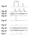
- Figs. 1A-1I are timing charts for explaining an example of those studies.
- the CCD is a device that effects photoelectric conversion of received fluorescent components by photoelectric converters such as photodiodes (PDs) and that transfers charges obtained by charge storage elements such as vertical transfer elements and horizontal transfer elements.
- the period of the photoelectric conversion by the photoelectric converters and the transfer of charges stored in the charge storage elements needs to be 1-2 msec.
- Fig. 1A is a timing chart of excitation pulse components, Fig. 1B that of fluorescent components, Fig. 1C that of electronic shutter signals, Fig. 1D that of readout signals, Fig. 1E that of charge amounts of photodiodes (PDs), Fig. 1F that of stored charge amounts of vertical elements, Fig. 1G that of transfer signals of horizontal elements, Fig. 1H that of transfer signals of vertical elements, and Fig. 1I that of readout of entire data.
- the period T indicates a period in which output of each signal is repeated at regular intervals.
- a fluorescence measuring apparatus is a fluorescence measuring apparatus for measuring fluorescent components emitted from a specimen corresponding to respective excitation pulse components projected toward the specimen, which comprises a photoelectric converter, a charge storage element, and a controller.
- the photoelectric converter implements photoelectric conversion of the fluorescent components emitted from the specimen corresponding to the respective excitation pulse components.
- the charge storage element stores a charge resulting from the photoelectric conversion by the photoelectric converter and transfers the stored charge.
- the controller outputs an electronic shutter signal for sweeping away the charge resulting from the photoelectric conversion by the photoelectric converter, a readout signal for reading the charge resulting from the photoelectric conversion, into the charge storage element, and a transfer signal for sequentially transferring the read charge.
- the controller outputs an electronic shutter signal corresponding to generation of a pulse component included in excitation light, outputs a readout signal corresponding to output of the electronic shutter signal, and outputs a transfer signal per at least two readout signals outputted.
- the controller outputs the electronic shutter signal per generation of an excitation pulse component and outputs the readout signal corresponding to output of this electronic shutter signal. For this reason, it becomes feasible to implement measurement of a fluorescent component corresponding to each excitation pulse component.
- the controller since the controller outputs the transfer signal per at least two readout signals outputted, a plurality of fluorescent components can be measured in a lump.
- the excitation pulse components and the fluorescent components each are preferably of a substantially identical waveform and identical period.
- the reason is that when the fluorescent components are of the substantially identical period, the number of fluorescence generations per predetermined time can be readily specified and it is easy to achieve synchronization with the electronic shutter signal.
- the fluorescent components are of the substantially identical waveform, it becomes easy to measure the same waveform part of each fluorescent component.
- the controller preferably outputs the electronic shutter signal and the readout signal so as to enable measurement of the same waveform part of each of the fluorescent components.
- the controller preferably outputs the electronic shutter signal and the readout signal so as to enable measurement of the same waveform part of each of the fluorescent components.
- the controller preferably outputs the electronic shutter signal and the transfer signal consecutively during a period before emission of a fluorescent component.
- the reason is that when the electronic shutter signal and the transfer signal are outputted before emission of a fluorescent component, i.e., before a start of measurement, it is feasible to prevent an unwanted charge from being stored in the photoelectric converter and in the charge storage element.
- the charge storage element may comprise a first charge storage element for directly receiving the charge from the photoelectric converter, and a second charge storage element for receiving the charge from the first charge storage element.
- the controller preferably outputs the transfer signal to the first charge storage element per predetermined number of readout signals outputted, and outputs the transfer signal consecutively to the second charge storage element. The reason is that when the transfer signal is consecutively outputted to the second charge storage element, storage of an unwanted charge in the second charge storage element can be effectively reduced.
- Figs. 1A-1I are timing charts for explaining a process of studies toward the present invention
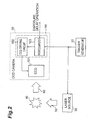
- Fig. 2 is an illustration showing a configuration of a measuring system including a fluorescence measuring apparatus according to the present invention
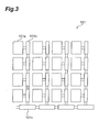
- Fig. 3 is an illustration showing a configuration of the CCD shown in Fig. 2;
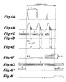
- Figs. 4A-4I are timing charts for explaining the operation in the fluorescence measuring apparatus according to the present invention.
- Fig. 2 is an illustration showing a configuration of a measuring system including a fluorescence measuring apparatus according to the present invention.
- the measuring system shown in this Fig. 2 is composed of a CCD camera 10 corresponding to the fluorescence measuring apparatus according to the present invention, a laser source 30, and a trigger generator 20.
- the CCD camera 10 includes a CCD 101, a CCD driving circuit 102, and a microcomputer 103.
- the CCD driving circuit 102 and the microcomputer 103 constitute a controller 100 of the fluorescence measuring apparatus.
- the CCD 101 is an interline transfer type CCD that measures a fluorescent component 60 emitted from a specimen 40, based on a command signal from the CCD driving circuit 102.
- the CCD 101 includes photodiodes (photoelectric converters) 101a, vertical transfer elements (first charge storage elements) 101b, and horizontal transfer elements (second charge storage elements) 101 c.
- Each photodiode 101a is a portion for storing a charge according to an amount of received light, and a plurality of photodiodes 101 a are arrayed on a substrate so as to form a desired light acceptance surface. Each photodiode 101 a sweeps away a stored charge with input of an electronic shutter signal from the CCD driving circuit 102, and moves a stored charge to a vertical transfer element 101b with input of a readout signal from the CCD driving circuit 102.
- the vertical transfer elements 101b being the first charge storage elements are provided corresponding to the respective photodiodes 101a.
- Each vertical transfer element 101b stores a charge moved from an associated photodiode 101a and transfers the charge to an adjacent vertical transfer element 101b according to need. More specifically, each vertical transfer element 101b sequentially transfers a charge stored therein, to a vertical transfer element 101b adjacent on the horizontal transfer element 101 c side with input of a transfer signal from the CCD driving circuit 102.
- the vertical transfer element 101b adjacent to the horizontal transfer element 101c transfers the charge thus transferred, to the horizontal transfer element 101 c.
- Each horizontal transfer element 101c is provided corresponding to a group of vertical transfer elements 101b in a column for transfer of charge from one to another.
- Each horizontal transfer element 101c stores a charge transferred from an associated column of vertical transfer elements 101b, and transfers the charge to an adjacent horizontal transfer element 101c.
- a horizontal transfer element 101c at the end finally stores the charge and, by reading the charge from the horizontal transfer element 101c at the end, the entire data resulting from photoelectric conversion by the photodiodes 101a can be read out.
- the CCD driving circuit 102 outputs the aforementioned electronic shutter signal, readout signal, and transfer signal, based on a command signal from the microcomputer 103.
- the microcomputer 103 outputs to the CCD driving circuit 102 command signals for output of the aforementioned electronic shutter signal, readout signal, and transfer signal, based on a trigger signal from the trigger generator 20. More specifically, the microcomputer 103 calculates timings of output of the electronic shutter signal, readout signal, and transfer signal, based on a trigger signal and an exposure delay operation of designating an exposure delay time of the CCD 101 relative to the trigger signal, and outputs them at the respective timings to the CCD driving circuit 102.
- These CCD driving circuit 102 and microcomputer 103 constitute the controller 100.
- the trigger generator 20 outputs a trigger signal to the laser source 30 and to the microcomputer 103.
- the laser source 30 emits an excitation pulse component 50 based on this trigger signal, toward a specimen 40.
- the specimen 40 emits fluorescent components 60 corresponding to respective excitation pulse components 50 and the CCD camera 10 measures these fluorescent components 60.
- Fig. 4A is a timing chart of excitation pulse components
- Fig. 4B that of fluorescent components
- Fig. 4C that of electronic shutter signals
- Fig. 4D that of readout signals
- Fig. 4E that of amounts of charges in the photodiodes (PDs)
- Fig. 4F that of amounts of charges stored in the vertical elements
- Fig. 4G that of transfer signals for the horizontal elements
- Fig. 4H that of transfer signals for the vertical elements
- Fig. 4I that of readout of entire data.
- the period T indicates a period in which output of each signal is repeated at regular intervals.
- the laser source 30 of Fig. 2 emits excitation pulse components 50 according to trigger signals from the trigger generator 20, toward the specimen 40 (see Fig. 4A).
- the trigger signals are so regulated that intervals of the excitation pulse components 50 become 1-2 msec.
- the specimen 40 releases fluorescent components 60 according to the excitation pulse components 50 thus emitted (see Fig. 4B).
- These fluorescent components 60 are optical components emitted according to properties of the specimen 40 and are generally of a nonlinear waveform as shown in Fig. 4B.
- An output delay time D of the electronic shutter signal relative to the trigger signal and the delay time W from the output of the electronic shutter signal to output of the readout signal are designated by the exposure delay operation fed to the microcomputer 103.
- the output delay time D and delay time W can be optionally set between 10 ⁇ sec and 400 ⁇ sec in consideration of a delay of fluorescent component 60 relative to excitation pulse component 50. Namely, when the output delay time D and the delay time W are optionally set, an exposed part (hatched portion in Fig. 4B) in the waveform of each fluorescent component 60 is optionally set and a spectrum of each fluorescent component 60 is made.
- the electronic shutter signals are outputted at regular intervals except for exposure periods from the CCD driving circuit 102 to the CCD 101, as shown in Fig. 4C. Namely, the electronic shutter signals are repeatedly outputted at regular intervals in each period T in Fig. 4C. Since the electronic shutter signal is a signal for sweeping away charges stored in the photodiodes 101 a of CCD 101, it is feasible to reduce storage of unwanted charges in the photodiodes 101a (see Fig. 4E).
- a stored charge ⁇ q resulting from photoelectric conversion in each photodiode 101a during an output delay time W is transferred to the associated vertical transfer element 101b with output of a readout signal (see Fig. 4C).
- the generation of excitation pulse component 50 is carried out t times, and the charge ⁇ q resulting from photoelectric conversion in each photodiode 101a is transferred t times to the vertical transfer element 101b.
- a transfer signal is fed to the vertical transfer elements 101b, and each vertical transfer element 101b successively transfers the stored charge ( ⁇ q ⁇ t) to an adjacent vertical transfer element 101b (see Fig. 4F).
- the charge thus transferred is then transferred to a horizontal transfer element 101c and is further transferred to an adjacent horizontal transfer element 101c to be read out.
- the charge thus read out is the charge ⁇ q stored t times, and, by dividing it by the number of operations t, it is feasible to obtain the charge ⁇ q corresponding to a fluorescent component 60 corresponding to one excitation pulse component 50.
- the transfer signals to the horizontal transfer elements 101c are always outputted at regular intervals from the CCD driving circuit 102. Namely, the transfer signals are outputted at regular intervals in the period T in Fig. 4G. Since this transfer signal is a signal for transferring the charge stored in each horizontal transfer element 101c, it is feasible to reduce storage of an unwanted charge in each horizontal transfer element 101c.
- the transfer signals to the vertical transfer elements 101b are outputted at regular intervals from the CCD driving circuit 102 before input of a trigger signal. Namely, the transfer signals are outputted at regular intervals in each period T in Fig. 4H. Since this transfer signal is a signal for transferring the charge stored in each vertical transfer element 101b, it is feasible to reduce storage of an unwanted charge in each vertical transfer element 101b.
- the microcomputer 103 and the CCD driving circuit 102 in the controller 100 output an electronic shutter signal per generation of an excitation pulse component 50 and output a readout signal corresponding to output of this electronic shutter signal. For this reason, it becomes feasible to perform measurement of a fluorescent component 60 corresponding to each excitation pulse component 50. Since the microcomputer 103 and the CCD driving circuit 102 output a transfer signal per predetermined number of readout signals outputted, it is feasible to measure the predetermined number of fluorescent components in a lump.
- the excitation pulse components 50 are generated so that fluorescent components 60 are of a substantially identical waveform and period. Since the fluorescent components 60 are of the substantially identical period, the number of fluorescences generated per predetermined time can be readily specified. Since the fluorescent components 60 are of the substantially identical waveform, it becomes easy to measure the identical waveform part which is equivalent among fluorescent components.
- the microcomputer 103 and the CCD driving circuit 102 as controller 100 calculate the output delay time D and the delay time W relative to the trigger signal so as to enable measurement of the same waveform part in each waveform of fluorescent component 60, and outputs the electronic shutter signals and the readout signals based thereon. Therefore, it is easy to measure the same waveform parts of respective fluorescent components emitted multiple times (t) and, by dividing the sum of the measurement results ( ⁇ q ⁇ t) by the predetermined number of times (t), the charge ⁇ q corresponding to the waveform part to be measured can be calculated.
- the present invention adopts the configuration wherein the controller outputs the electronic shutter signals corresponding to the respective excitation pulse component emitted toward the specimen and outputs the readout signals corresponding to the output of the electronic shutter signals, the invention enables the measurement of the fluorescent component corresponding to each excitation pulse component. Since the controller outputs the transfer signal per predetermined number of readout signals outputted, the predetermined number of fluorescent components can be measured in a lump. Therefore, we obtained the fluorescence measuring apparatus capable of measuring the fluorescent components emitted from the specimen corresponding to excitation pulse components, by use of the CCD.
Landscapes
- Physics & Mathematics (AREA)
- Spectroscopy & Molecular Physics (AREA)
- General Physics & Mathematics (AREA)
- Health & Medical Sciences (AREA)
- Life Sciences & Earth Sciences (AREA)
- Biochemistry (AREA)
- Multimedia (AREA)
- Nuclear Medicine, Radiotherapy & Molecular Imaging (AREA)
- Engineering & Computer Science (AREA)
- Chemical & Material Sciences (AREA)
- Analytical Chemistry (AREA)
- Signal Processing (AREA)
- General Health & Medical Sciences (AREA)
- Immunology (AREA)
- Pathology (AREA)
- Investigating, Analyzing Materials By Fluorescence Or Luminescence (AREA)
- Transforming Light Signals Into Electric Signals (AREA)
- Photometry And Measurement Of Optical Pulse Characteristics (AREA)
Abstract
Description
Claims (5)
- A fluorescence measuring apparatus for emitting a plurality of excitation pulse components toward a specimen and for measuring fluorescent components emitted from the specimen corresponding to the respective excitation pulse components, said fluorescence measuring apparatus comprising:wherein said controller outputs the electronic shutter signal corresponding to generation of a pulse component included in the excitation light, outputs the readout signal corresponding to output of said electronic shutter signal, and outputs the transfer signal per at least two readout signals outputted.a photoelectric converter for implementing photoelectric conversion of a fluorescent component emitted from the specimen;a charge storage element for storing a charge resulting from the photoelectric conversion by said photoelectric converter and for transferring the charge stored; anda controller for outputting an electronic shutter signal for sweeping away the charge resulting from the photoelectric conversion by said photoelectric converter, a readout signal for reading the charge resulting from the photoelectric conversion, into said charge storage element, and a transfer signal for sequentially transferring the charge read,
- A fluorescence measuring apparatus according to claim 1, wherein the excitation pulse components are of a substantially identical waveform and identical period, and
wherein the fluorescent components are of a substantially identical waveform and identical period. - A fluorescence measuring apparatus according to claim 2, wherein said controller outputs the electronic shutter signal and the readout signal so as to enable measurement of an identical waveform part in each of the fluorescent components.
- A fluorescence measuring apparatus according to claim 1, wherein said controller outputs the electronic shutter signal and the transfer signal consecutively before emission of the fluorescent components.
- A fluorescence measuring apparatus according to claim 1, wherein said charge storage element comprises a first charge storage element for directly receiving the charge from said photoelectric converter, and a second charge storage element for receiving the charge from said first charge storage element, and
wherein said controller outputs the transfer signal per predetermined number of readout signals outputted, to said first charge storage element and consecutively outputs the transfer signal to said second charge storage element.
Applications Claiming Priority (3)
| Application Number | Priority Date | Filing Date | Title |
|---|---|---|---|
| JP2002288848A JP4188653B2 (en) | 2002-10-01 | 2002-10-01 | Fluorescence measuring device |
| JP2002288848 | 2002-10-01 | ||
| PCT/JP2003/012609 WO2004031748A1 (en) | 2002-10-01 | 2003-10-01 | Fluorescence measuring device |
Publications (3)
| Publication Number | Publication Date |
|---|---|
| EP1550857A1 true EP1550857A1 (en) | 2005-07-06 |
| EP1550857A4 EP1550857A4 (en) | 2006-12-20 |
| EP1550857B1 EP1550857B1 (en) | 2010-02-24 |
Family
ID=32063695
Family Applications (1)
| Application Number | Title | Priority Date | Filing Date |
|---|---|---|---|
| EP03748660A Expired - Lifetime EP1550857B1 (en) | 2002-10-01 | 2003-10-01 | Fluorescence measuring device |
Country Status (7)
| Country | Link |
|---|---|
| US (1) | US20060124863A1 (en) |
| EP (1) | EP1550857B1 (en) |
| JP (1) | JP4188653B2 (en) |
| CN (1) | CN100462713C (en) |
| AU (1) | AU2003268725A1 (en) |
| DE (1) | DE60331454D1 (en) |
| WO (1) | WO2004031748A1 (en) |
Cited By (1)
| Publication number | Priority date | Publication date | Assignee | Title |
|---|---|---|---|---|
| EP1925930A1 (en) * | 2003-02-13 | 2008-05-28 | Hamamatsu Photonics K.K. | Flourescence correlation spectroscopy analyser |
Families Citing this family (5)
| Publication number | Priority date | Publication date | Assignee | Title |
|---|---|---|---|---|
| JP4662123B2 (en) * | 2004-09-24 | 2011-03-30 | 横河電機株式会社 | Laser confocal microscope system |
| CN101472076B (en) * | 2007-12-28 | 2010-09-29 | 鸿富锦精密工业(深圳)有限公司 | Image shooting device and shooting control method thereof |
| WO2012111093A1 (en) * | 2011-02-15 | 2012-08-23 | 有限会社ワイ・システムズ | Method and device for measuring carrier lifetime |
| KR102126694B1 (en) * | 2018-06-01 | 2020-06-25 | 주식회사 수젠텍 | Time resolved fluorescence analyzer |
| EP3937780A4 (en) * | 2019-03-14 | 2022-12-07 | InSilixa, Inc. | METHODS AND SYSTEMS FOR TIME RESOLVED FLUORESCENCE-BASED DETECTION |
Family Cites Families (11)
| Publication number | Priority date | Publication date | Assignee | Title |
|---|---|---|---|---|
| JPS5795771A (en) * | 1980-12-05 | 1982-06-14 | Fuji Photo Film Co Ltd | Solid-state image pickup device |
| JPS59104519A (en) * | 1982-12-07 | 1984-06-16 | Hamamatsu Photonics Kk | Measuring device of high-speed repetitive pulsed light |
| JP2694200B2 (en) * | 1988-03-08 | 1997-12-24 | 日本分光株式会社 | Multi-channel fluorescence decay waveform measuring device |
| US5323008A (en) * | 1992-03-23 | 1994-06-21 | Diatron Corporation | Fluorometer detection system |
| JP3281755B2 (en) * | 1995-04-05 | 2002-05-13 | 三菱重工業株式会社 | Measurement device by laser induced fluorescence method |
| DE19651101A1 (en) * | 1996-12-09 | 1998-06-10 | Giesecke & Devrient Gmbh | Device and method for the detection of fluorescent and phosphorescent light |
| US5821547A (en) * | 1997-03-10 | 1998-10-13 | Talmi; Yair | Temporal filter using interline charged coupled device |
| JPH11164210A (en) * | 1997-11-28 | 1999-06-18 | Nikon Corp | Solid-state imaging device for motion detection |
| US6037584A (en) * | 1998-05-08 | 2000-03-14 | Hewlett-Packard Company | Optical scanner including exposure control |
| JP2001339638A (en) * | 2000-05-26 | 2001-12-07 | Hamamatsu Photonics Kk | Streak camera device |
| MXPA04002498A (en) * | 2001-09-19 | 2005-04-11 | Joule Microsystems Canada Inc | A spectrometer incorporating signal matched filtering. |
-
2002
- 2002-10-01 JP JP2002288848A patent/JP4188653B2/en not_active Expired - Fee Related
-
2003
- 2003-10-01 WO PCT/JP2003/012609 patent/WO2004031748A1/en not_active Ceased
- 2003-10-01 CN CNB2003801007671A patent/CN100462713C/en not_active Expired - Fee Related
- 2003-10-01 US US10/529,653 patent/US20060124863A1/en not_active Abandoned
- 2003-10-01 EP EP03748660A patent/EP1550857B1/en not_active Expired - Lifetime
- 2003-10-01 AU AU2003268725A patent/AU2003268725A1/en not_active Abandoned
- 2003-10-01 DE DE60331454T patent/DE60331454D1/en not_active Expired - Lifetime
Cited By (2)
| Publication number | Priority date | Publication date | Assignee | Title |
|---|---|---|---|---|
| EP1925930A1 (en) * | 2003-02-13 | 2008-05-28 | Hamamatsu Photonics K.K. | Flourescence correlation spectroscopy analyser |
| US7737389B2 (en) | 2003-02-13 | 2010-06-15 | Hamamatsu Photonics K.K. | Image pickup device including photodetection surface and transfer control arrangement |
Also Published As
| Publication number | Publication date |
|---|---|
| US20060124863A1 (en) | 2006-06-15 |
| CN1695053A (en) | 2005-11-09 |
| EP1550857A4 (en) | 2006-12-20 |
| EP1550857B1 (en) | 2010-02-24 |
| DE60331454D1 (en) | 2010-04-08 |
| WO2004031748A1 (en) | 2004-04-15 |
| JP4188653B2 (en) | 2008-11-26 |
| JP2004125556A (en) | 2004-04-22 |
| CN100462713C (en) | 2009-02-18 |
| AU2003268725A1 (en) | 2004-04-23 |
Similar Documents
| Publication | Publication Date | Title |
|---|---|---|
| JP2002315022A (en) | 3D image detection device | |
| US8948342B2 (en) | X-ray imaging apparatus and measurement method | |
| JP4330751B2 (en) | Radiographic image acquisition method and apparatus, and cell interval detection method and apparatus therefor | |
| JP2016506492A (en) | Method for generating an image with depth information and an image sensor | |
| EP1550857B1 (en) | Fluorescence measuring device | |
| RU2446613C2 (en) | Device for recording images generated using radiation | |
| GB2105035A (en) | Instrument for measuring light emission | |
| US6683676B1 (en) | Three-dimensional image capturing device | |
| RU2089932C1 (en) | Device to view objects | |
| JP4369575B2 (en) | 3D image detection device | |
| US4703177A (en) | Arrangement for the production of X-ray pictures by computer radiography | |
| Sandel et al. | Effect of phosphor persistence on photometry with image intensifiers and integrating readout devices | |
| GB2323237A (en) | Interline charge coupled device | |
| RU63599U1 (en) | PERSONNEL ELECTRON-OPTICAL RECORDER OF PULSE LIGHT RADIATION | |
| KR910007703B1 (en) | Measuring method for blooming for a solid photographing element and the apparatus of the same | |
| JP2016116754A (en) | Radiographic apparatus and control method thereof | |
| US6982761B1 (en) | Device for capturing three-dimensional images with independently controllable groups of photoelectric conversion elements | |
| US7683952B2 (en) | Optical image information detecting apparatus | |
| US20120193552A1 (en) | Fluorescence lifetime imaging | |
| SU1574014A1 (en) | Multichannel fluorimeter | |
| JP2729276B2 (en) | Scintillation camera | |
| JP2004298404A (en) | Autofluorescent endoscope device | |
| JP2002278005A (en) | Radiation image reader | |
| RU2657292C1 (en) | Method of active pulse vision | |
| CN118613744A (en) | Measuring device |
Legal Events
| Date | Code | Title | Description |
|---|---|---|---|
| PUAI | Public reference made under article 153(3) epc to a published international application that has entered the european phase |
Free format text: ORIGINAL CODE: 0009012 |
|
| 17P | Request for examination filed |
Effective date: 20050422 |
|
| AK | Designated contracting states |
Kind code of ref document: A1 Designated state(s): AT BE BG CH CY CZ DE DK EE ES FI FR GB GR HU IE IT LI LU MC NL PT RO SE SI SK TR |
|
| AX | Request for extension of the european patent |
Extension state: AL LT LV MK |
|
| DAX | Request for extension of the european patent (deleted) | ||
| RBV | Designated contracting states (corrected) |
Designated state(s): CH DE FI FR GB LI SE |
|
| RIC1 | Information provided on ipc code assigned before grant |
Ipc: H04N 5/335 20060101ALI20061106BHEP Ipc: G01N 21/64 20060101AFI20040416BHEP Ipc: G01J 1/42 20060101ALI20061106BHEP |
|
| A4 | Supplementary search report drawn up and despatched |
Effective date: 20061117 |
|
| 17Q | First examination report despatched |
Effective date: 20070426 |
|
| GRAP | Despatch of communication of intention to grant a patent |
Free format text: ORIGINAL CODE: EPIDOSNIGR1 |
|
| RIC1 | Information provided on ipc code assigned before grant |
Ipc: H04N 5/335 20060101ALI20090728BHEP Ipc: H04N 5/321 20060101ALI20090728BHEP Ipc: G01J 1/42 20060101ALI20090728BHEP Ipc: G01J 3/44 20060101ALI20090728BHEP Ipc: G01N 21/64 20060101AFI20090728BHEP Ipc: G01J 3/28 20060101ALI20090728BHEP |
|
| GRAS | Grant fee paid |
Free format text: ORIGINAL CODE: EPIDOSNIGR3 |
|
| GRAA | (expected) grant |
Free format text: ORIGINAL CODE: 0009210 |
|
| RAP1 | Party data changed (applicant data changed or rights of an application transferred) |
Owner name: HAMAMATSU PHOTONICS K.K. |
|
| AK | Designated contracting states |
Kind code of ref document: B1 Designated state(s): CH DE FI FR GB LI SE |
|
| REG | Reference to a national code |
Ref country code: GB Ref legal event code: FG4D |
|
| REG | Reference to a national code |
Ref country code: CH Ref legal event code: EP |
|
| RAP2 | Party data changed (patent owner data changed or rights of a patent transferred) |
Owner name: HAMAMATSU PHOTONICS K.K. |
|
| REF | Corresponds to: |
Ref document number: 60331454 Country of ref document: DE Date of ref document: 20100408 Kind code of ref document: P |
|
| REG | Reference to a national code |
Ref country code: CH Ref legal event code: NV Representative=s name: KIRKER & CIE S.A. |
|
| REG | Reference to a national code |
Ref country code: SE Ref legal event code: TRGR |
|
| PLBE | No opposition filed within time limit |
Free format text: ORIGINAL CODE: 0009261 |
|
| STAA | Information on the status of an ep patent application or granted ep patent |
Free format text: STATUS: NO OPPOSITION FILED WITHIN TIME LIMIT |
|
| 26N | No opposition filed |
Effective date: 20101125 |
|
| PGFP | Annual fee paid to national office [announced via postgrant information from national office to epo] |
Ref country code: GB Payment date: 20130925 Year of fee payment: 11 |
|
| PGFP | Annual fee paid to national office [announced via postgrant information from national office to epo] |
Ref country code: FR Payment date: 20131009 Year of fee payment: 11 Ref country code: SE Payment date: 20131011 Year of fee payment: 11 Ref country code: CH Payment date: 20131014 Year of fee payment: 11 Ref country code: DE Payment date: 20130925 Year of fee payment: 11 |
|
| PGFP | Annual fee paid to national office [announced via postgrant information from national office to epo] |
Ref country code: FI Payment date: 20131010 Year of fee payment: 11 |
|
| REG | Reference to a national code |
Ref country code: DE Ref legal event code: R119 Ref document number: 60331454 Country of ref document: DE |
|
| REG | Reference to a national code |
Ref country code: CH Ref legal event code: PL |
|
| REG | Reference to a national code |
Ref country code: SE Ref legal event code: EUG |
|
| GBPC | Gb: european patent ceased through non-payment of renewal fee |
Effective date: 20141001 |
|
| PG25 | Lapsed in a contracting state [announced via postgrant information from national office to epo] |
Ref country code: CH Free format text: LAPSE BECAUSE OF NON-PAYMENT OF DUE FEES Effective date: 20141031 Ref country code: GB Free format text: LAPSE BECAUSE OF NON-PAYMENT OF DUE FEES Effective date: 20141001 Ref country code: LI Free format text: LAPSE BECAUSE OF NON-PAYMENT OF DUE FEES Effective date: 20141031 Ref country code: DE Free format text: LAPSE BECAUSE OF NON-PAYMENT OF DUE FEES Effective date: 20150501 Ref country code: FI Free format text: LAPSE BECAUSE OF NON-PAYMENT OF DUE FEES Effective date: 20141001 Ref country code: SE Free format text: LAPSE BECAUSE OF NON-PAYMENT OF DUE FEES Effective date: 20141002 |
|
| REG | Reference to a national code |
Ref country code: FR Ref legal event code: ST Effective date: 20150630 |
|
| PG25 | Lapsed in a contracting state [announced via postgrant information from national office to epo] |
Ref country code: FR Free format text: LAPSE BECAUSE OF NON-PAYMENT OF DUE FEES Effective date: 20141031 |