EP1550167B1 - Illuminator assembly - Google Patents
Illuminator assembly Download PDFInfo
- Publication number
- EP1550167B1 EP1550167B1 EP03752632A EP03752632A EP1550167B1 EP 1550167 B1 EP1550167 B1 EP 1550167B1 EP 03752632 A EP03752632 A EP 03752632A EP 03752632 A EP03752632 A EP 03752632A EP 1550167 B1 EP1550167 B1 EP 1550167B1
- Authority
- EP
- European Patent Office
- Prior art keywords
- lens
- heat sink
- illuminator assembly
- light source
- recess
- Prior art date
- Legal status (The legal status is an assumption and is not a legal conclusion. Google has not performed a legal analysis and makes no representation as to the accuracy of the status listed.)
- Expired - Lifetime
Links
Images


Classifications
-
- F—MECHANICAL ENGINEERING; LIGHTING; HEATING; WEAPONS; BLASTING
- F21—LIGHTING
- F21V—FUNCTIONAL FEATURES OR DETAILS OF LIGHTING DEVICES OR SYSTEMS THEREOF; STRUCTURAL COMBINATIONS OF LIGHTING DEVICES WITH OTHER ARTICLES, NOT OTHERWISE PROVIDED FOR
- F21V29/00—Protecting lighting devices from thermal damage; Cooling or heating arrangements specially adapted for lighting devices or systems
- F21V29/50—Cooling arrangements
- F21V29/70—Cooling arrangements characterised by passive heat-dissipating elements, e.g. heat-sinks
- F21V29/71—Cooling arrangements characterised by passive heat-dissipating elements, e.g. heat-sinks using a combination of separate elements interconnected by heat-conducting means, e.g. with heat pipes or thermally conductive bars between separate heat-sink elements
-
- A—HUMAN NECESSITIES
- A61—MEDICAL OR VETERINARY SCIENCE; HYGIENE
- A61C—DENTISTRY; APPARATUS OR METHODS FOR ORAL OR DENTAL HYGIENE
- A61C19/00—Dental auxiliary appliances
- A61C19/003—Apparatus for curing resins by radiation
- A61C19/004—Hand-held apparatus, e.g. guns
-
- A—HUMAN NECESSITIES
- A61—MEDICAL OR VETERINARY SCIENCE; HYGIENE
- A61C—DENTISTRY; APPARATUS OR METHODS FOR ORAL OR DENTAL HYGIENE
- A61C19/00—Dental auxiliary appliances
- A61C19/06—Implements for therapeutic treatment
- A61C19/063—Medicament applicators for teeth or gums, e.g. treatment with fluorides
- A61C19/066—Bleaching devices; Whitening agent applicators for teeth, e.g. trays or strips
-
- F—MECHANICAL ENGINEERING; LIGHTING; HEATING; WEAPONS; BLASTING
- F21—LIGHTING
- F21V—FUNCTIONAL FEATURES OR DETAILS OF LIGHTING DEVICES OR SYSTEMS THEREOF; STRUCTURAL COMBINATIONS OF LIGHTING DEVICES WITH OTHER ARTICLES, NOT OTHERWISE PROVIDED FOR
- F21V29/00—Protecting lighting devices from thermal damage; Cooling or heating arrangements specially adapted for lighting devices or systems
- F21V29/50—Cooling arrangements
- F21V29/70—Cooling arrangements characterised by passive heat-dissipating elements, e.g. heat-sinks
- F21V29/74—Cooling arrangements characterised by passive heat-dissipating elements, e.g. heat-sinks with fins or blades
- F21V29/77—Cooling arrangements characterised by passive heat-dissipating elements, e.g. heat-sinks with fins or blades with essentially identical diverging planar fins or blades, e.g. with fan-like or star-like cross-section
- F21V29/773—Cooling arrangements characterised by passive heat-dissipating elements, e.g. heat-sinks with fins or blades with essentially identical diverging planar fins or blades, e.g. with fan-like or star-like cross-section the planes containing the fins or blades having the direction of the light emitting axis
-
- H—ELECTRICITY
- H01—ELECTRIC ELEMENTS
- H01L—SEMICONDUCTOR DEVICES NOT COVERED BY CLASS H10
- H01L33/00—Semiconductor devices with at least one potential-jump barrier or surface barrier specially adapted for light emission; Processes or apparatus specially adapted for the manufacture or treatment thereof or of parts thereof; Details thereof
- H01L33/48—Semiconductor devices with at least one potential-jump barrier or surface barrier specially adapted for light emission; Processes or apparatus specially adapted for the manufacture or treatment thereof or of parts thereof; Details thereof characterised by the semiconductor body packages
- H01L33/64—Heat extraction or cooling elements
- H01L33/647—Heat extraction or cooling elements the elements conducting electric current to or from the semiconductor body
-
- F—MECHANICAL ENGINEERING; LIGHTING; HEATING; WEAPONS; BLASTING
- F21—LIGHTING
- F21Y—INDEXING SCHEME ASSOCIATED WITH SUBCLASSES F21K, F21L, F21S and F21V, RELATING TO THE FORM OR THE KIND OF THE LIGHT SOURCES OR OF THE COLOUR OF THE LIGHT EMITTED
- F21Y2115/00—Light-generating elements of semiconductor light sources
- F21Y2115/10—Light-emitting diodes [LED]
-
- H—ELECTRICITY
- H01—ELECTRIC ELEMENTS
- H01L—SEMICONDUCTOR DEVICES NOT COVERED BY CLASS H10
- H01L2224/00—Indexing scheme for arrangements for connecting or disconnecting semiconductor or solid-state bodies and methods related thereto as covered by H01L24/00
- H01L2224/01—Means for bonding being attached to, or being formed on, the surface to be connected, e.g. chip-to-package, die-attach, "first-level" interconnects; Manufacturing methods related thereto
- H01L2224/42—Wire connectors; Manufacturing methods related thereto
- H01L2224/47—Structure, shape, material or disposition of the wire connectors after the connecting process
- H01L2224/48—Structure, shape, material or disposition of the wire connectors after the connecting process of an individual wire connector
- H01L2224/4805—Shape
- H01L2224/4809—Loop shape
- H01L2224/48091—Arched
-
- H—ELECTRICITY
- H01—ELECTRIC ELEMENTS
- H01L—SEMICONDUCTOR DEVICES NOT COVERED BY CLASS H10
- H01L2224/00—Indexing scheme for arrangements for connecting or disconnecting semiconductor or solid-state bodies and methods related thereto as covered by H01L24/00
- H01L2224/01—Means for bonding being attached to, or being formed on, the surface to be connected, e.g. chip-to-package, die-attach, "first-level" interconnects; Manufacturing methods related thereto
- H01L2224/42—Wire connectors; Manufacturing methods related thereto
- H01L2224/47—Structure, shape, material or disposition of the wire connectors after the connecting process
- H01L2224/48—Structure, shape, material or disposition of the wire connectors after the connecting process of an individual wire connector
- H01L2224/481—Disposition
- H01L2224/48135—Connecting between different semiconductor or solid-state bodies, i.e. chip-to-chip
- H01L2224/48137—Connecting between different semiconductor or solid-state bodies, i.e. chip-to-chip the bodies being arranged next to each other, e.g. on a common substrate
-
- H—ELECTRICITY
- H01—ELECTRIC ELEMENTS
- H01L—SEMICONDUCTOR DEVICES NOT COVERED BY CLASS H10
- H01L33/00—Semiconductor devices with at least one potential-jump barrier or surface barrier specially adapted for light emission; Processes or apparatus specially adapted for the manufacture or treatment thereof or of parts thereof; Details thereof
- H01L33/48—Semiconductor devices with at least one potential-jump barrier or surface barrier specially adapted for light emission; Processes or apparatus specially adapted for the manufacture or treatment thereof or of parts thereof; Details thereof characterised by the semiconductor body packages
- H01L33/64—Heat extraction or cooling elements
- H01L33/642—Heat extraction or cooling elements characterized by the shape
-
- Y—GENERAL TAGGING OF NEW TECHNOLOGICAL DEVELOPMENTS; GENERAL TAGGING OF CROSS-SECTIONAL TECHNOLOGIES SPANNING OVER SEVERAL SECTIONS OF THE IPC; TECHNICAL SUBJECTS COVERED BY FORMER USPC CROSS-REFERENCE ART COLLECTIONS [XRACs] AND DIGESTS
- Y10—TECHNICAL SUBJECTS COVERED BY FORMER USPC
- Y10S—TECHNICAL SUBJECTS COVERED BY FORMER USPC CROSS-REFERENCE ART COLLECTIONS [XRACs] AND DIGESTS
- Y10S362/00—Illumination
- Y10S362/80—Light emitting diode
Definitions
- the present invention relates generally and in various embodiments to illuminator assemblies. More specifically, the present invention relates generally and in various embodiments to illuminator assemblies including heat sinks.
- Compact sources of light are needed for a variety of applications in dentistry and surgery such as surgical cutting, curing of dental composite materials, and activating tooth-whitening materials, for example.
- dentists may use high intensity light for correcting diseases or defects in hard tissues such as the enamel and dentin portions of the teeth where drills are normally used.
- dentists may use high intensity light for curing a variety of resins and composites in a patient's mouth and for bleaching teeth.
- Dental composite curing and teeth bleaching application generally require sources of light that emit light having wavelengths in the ultra violet (UV) portion of the spectrum.
- Surgeons may use high power/high intensity sources of light in certain applications for correcting diseases or defects in soft tissues for which scalpels and other similar surgical cutting instruments are normally used.
- Cutting applications also may require sources of light that emit light having wavelengths in various portions of the spectrum.
- US2002/0113244A1 describes a high power illumination assembly comprising an LED package.
- the LED is located on a large cathode which acts as a heat sink, conducting heat away from the LED.
- the cathode sits within a lead frame comprising an annular anode and a liquid crystal polymer, which provides for thermal conduction whilst electrically insulating the anode from the cathode.
- a dome-shaped lens is seated over the lead frame, providing protection for the LED package as well as collecting and shaping light emitted by the LED.
- the present invention is directed to an apparatus, as recited in claim 1, that includes a lens having a light entrance end forming a recess, a heat sink having an end portion facing the recess, and a light source positioned to transmit light via the recess into the lens in thermal communication with the heat sink, wherein heat generated by the light source is conducted to the heat sink.
- the lens is a non-imaging lens, such as a total internal reflection (TIR) lens, and has a rearward portion defining an outer surface which tapers to a smaller diameter in the direction of the heat sink.
- TIR total internal reflection
- the lens holder has a front portion for receiving the lens with a tapered inner surface to accommodate it.
- the lens holder also has a rear portion for receiving an end portion of the heat sink on which the light source is mounted.
- the illuminator assembly of the present invention provides an alternative compact light source to those known in the art.
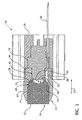
- FIG. 1 is a sectioned assembly view of one embodiment of an illuminator assembly 10 in accordance with the present invention.
- the illuminator assembly 10 may comprise a variety of components such as a lens 12, a lens holder 14, a first heat sink 16, and, optionally, a second heat sink 18, for example.
- the heat sink 16, 18 may be any substance or device for the absorption or dissipation of heat generated from a process, electronic device, or light source, for example.
- the lens 12 and the first heat sink 16 may be coaxially aligned.
- the first heat sink 16 and the lens holder 14 also may be coaxially aligned.
- the illuminator assembly 10 may include a housing 170 (e.g. , see Figures 22, 23) extending about the first heat sink 16 and is in coaxial relation therewith. Further, the lens holder 14 may include an end portion that is received into the housing 170. Also, in one embodiment of the present invention, the first heat sink 16 may act as a primary heat sink for conducting heat away from the light source while the second heat sink 18 may act as a secondary heat sink for conducting heat away from the first heat sink 16.
- the lens 12 may include, for example, a light entrance end 20 forming a recess 22 and a light exit end 24 where light generated by a light source assembly 50 ( e.g. , see Figures 9, 10, 17) located on an end portion 30 of the first heat sink 16 is emitted.
- the lens 12 also may include a forward cylindrical portion 25 and a rearward portion 26 extending about the recess 22 that defines an outer surface 28 that tapers in a direction 27 toward the first heat sink 16 and/or the second heat sink 18.
- the lens holder 14 may include a front portion 32 that extends about the recess 22 of the lens 12 and may include a rear portion 34 for receiving the end portion 30 of the first heat sink 16. Thus the end portion 30 of the first heat sink 16 projects endwise into the lens holder 14.
- the lens holder 14 also may define an inner wall 35 that tapers in a direction 27 toward the first heat sink 16 and/or the second heat sink 18.
- the lens's tapering outer surface 28 also may extend into the tapered portion of the lens holder's inner wall 35.
- the lens's outer surface 28 also tapers in the direction 27 toward the first heat sink 16 and/or the second heat sink 18 and is oriented in adjacent relation to the lens holder's 14 inner wall 35.
- the illuminator assembly 10 in accordance with one embodiment of the present invention also may include a first current carrying wire 36 that extends between the lens holder 14 and the first heat sink 16 and/or the second heat sink 18.
- the first current carrying wire 36 may be used to supply electrical current to the light source.
- the first current carrying wire 36 may be received in an opening 38 formed in the lens holder 14.
- Figures 2 and 3 show a side view and an end view A-A, respectively, of one embodiment of the lens 12 component of the illuminator assembly 10 according to the present invention.
- the lens 12 may include, for example, the light entrance end 20 forming the recess 22 and the light exit end 24 for emitting the light generated by the light source assembly 50.
- the lens 12 has a forward cylindrical portion 25 and a rearward arcuate portion 26 that extends about the recess 22.
- the arcuate portion 26 defines an outer surface 28 that tapers in the direction 27 toward the first heat sink 16 and/or the second heat sink 18.
- the recess 22 may be re-entrant into the lens 12.
- the lens 12 may include a rearward wall 23 that is concave in a direction 21 toward the recess 22.
- the recess 22 may be filled with a light transmitting material, such as, for example, a light transmitting plastic material.
- the recess 22 may contain an optical plastic material having a predetermined index of refraction.
- the index of refraction of the optical plastic material may be substantially the same as the index of refraction as the lens 12 material.
- the optical plastic material contained in the recess 22 may be curable by light having a wavelength in the ultra-violet (UV) portion of the optical spectrum, for example.
- the lens 12, for example may be a non-imaging lens and may be formed of a variety of materials such as optical polycarbonate, for example.
- the lens 12 may be a total internal reflection (TIR) lens.
- TIR total internal reflection
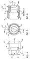
- FIGS 4, 5, and 6 are side, end, and sectioned views, respectively, of one embodiment of the lens holder 14 component of the illuminator assembly 10 according to the present invention.
- the front portion 32 of the lens holder 14 defines a first cavity 33 for receiving the light entrance end 20 of the lens 12.
- the front portion 32 and the inner wall 35 of the lens holder 14 extend about the recess 22 of the lens 12.
- the rear portion 34 of the lens holder 14 defines a second cavity 37 for receiving the end portion 30 of the first heat sink 16 such that the end portion 30 of the first heat sink 16 including the light source assembly 50 projects endwise into the lens holder 14.
- the inner wall 35 of the lens holder 14 tapers to a smaller diameter in the direction 27 toward the first heat sink 16 and/or the second heat sink 18.
- the tapering outer surface 28 of the lens 12 extends into the tapered inner wall 25 portion of the lens holder 14.
- the outer surface 28 of the lens 12 is in adjacent relation to the inner wall 35 of the lens holder 14 and is tapered toward the first heat sink 16 and/or the second heat sink 18.
- the lens holder 14 also defines an opening 38 for receiving the first current carrying wire 36 therethrough.
- the lens holder 14 may be formed of Teflon, for example.
- Figures 7 and 8 are side and end views, respectively, of one embodiment of the first heat sink 16 component, according to the present invention, where Figure 7 is a sectioned view.
- the first heat sink 16 comprises a body portion 40, which may include an end portion 30 that faces the recess 22 portion of the lens 12.
- the end portion 30 is received into the second cavity 37 defined by the rear portion 34 of the lens holder 14.
- the end portion 30 also includes a face portion 31 for receiving the light source assembly 50 ( e.g. , see Figures 9 and 10).
- the face portion 31 of the first heat sink 16 may be gold plated and/or gold/nickel plated such that the face portion 31 is rendered suitable for attaching a semiconductor die or chip directly thereon and is rendered suitable for accepting wire bonds thereon.
- the light source assembly 50 is placed in thermal communication or in contact with the body portion 40 or end portion 30 of the first heat sink 16 and/or with the second heat sink 18.
- the first heat sink 16 acts a thermal conductor and its body portion 40 conducts heat away from the light source assembly 50.
- the body portion 40 of the first heat sink 16 also may transmit heat generated by the light source assembly 50 to the second heat sink 18 formed about the first heat sink 16.
- the body portion 40 of the first heat sink 16 also may include a channel 42 formed therein for receiving the first current carrying wire 36 so that electrical current may be supplied to the light source assembly 50 located on the face portion 31 of the first heat sink 16.
- the body portion 40 of the first heat sink 16 also may include an elongated portion 44, which may define a hollow portion 46 for receiving a second wire 48 ( e.g. , see Figure 9) therein.
- the body portion 40 of the first heat sink 16 may be formed of a variety of materials that are thermally conductive and/or electrically conductive materials such as, for example, aluminum, brass, bronze, copper, gold, nickel, platinum, steel, and the like, and/or any combinations of such materials including plated forms of such materials.
- the first heat sink 16 may be nickel or gold plated copper.
- the first heat sink 16 may be nickel or gold plated on portions of the body 40 to make electrical connections.
- the first heat sink 16 and the second heat sink 18 may be integrally formed.
- Figures 9 and 10 are also side and end views, respectively, of one embodiment of the first heat sink 16 component according to the present invention.
- the first heat sink 16 is shown wired to one embodiment of a light source assembly 50 according to the present invention.
- the light source assembly 50 may comprise, for example, a light source 52 including a plurality or array of light emitting diodes 93 (LEDs) in semiconductor die form, and may be arranged in a predetermined manner as shown.
- the light source assembly 50 is located on the face portion 31 of the first heat sink 16.
- the light source assembly 50 is positioned such that it faces the recess 22 formed on the light entrance portion 20 of the lens 12. Accordingly, the light emitted from the light source 52 is transmitted via the recess 22 and the material contained in the recess 22.
- the light source assembly 50 may comprise one or more LED semiconductor die(s) 93 die bonded to the face portion 31 of the end portion 30 of the first heat sink 16.
- the light source assembly 50 also may include an interface board 56 for making an appropriate physical electrical connection between a light source power supply and the light source 52.
- the first wire 36 is electrically connected to the interface board 56 at solder connection 58.
- the first wire 36 is connected to a light source power supply.
- the first wire 36 may supply electrical current to the light source 52 or may provide a return path ( e.g. , ground) for the light source 52.
- the interface board 56 also may serve for receiving wire bonds, e.g., from the LED semiconductor dies 93.
- a second wire 48 may be electrically attached to the elongated portion 44 of the first heat sink 16 by any well known means of attachment, such as a solder connection 54, a weld, screw, and the like.
- the second wire 48 also may be attached directly to an outer wall of the body portion as shown in Figure 9.
- the body portion 40 of the first heat sink 16 may be connected to an electrical connection of the light source assembly 50 through the second wire 48.
- the electrical connection may be used to supply power or a return path (e.g. , ground) through the second wire 48.
- a return path e.g. , ground
- the light source 52 may be coated with an optically transmissive encapsulating material 60, such as UV curable adhesive optical acrylic material, for example.
- an optically transmissive encapsulating material 60 such as UV curable adhesive optical acrylic material, for example.
- the encapsulating material 60 is placed in a mold such that its shape conforms to the surface contour of the recess 22 formed in the light entrance end 20 of the lens 12. Conforming the shape of the encapsulating material 60 to the contour of the recess 22 helps to transmit the light generated by the light source 52 to the lens 12 and through the light exit end 24 of the lens 12.
- the light source assembly 50 will be discussed below in more detail with respect to Figures 15-21.
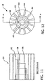
- Figures 11 and 12 are sectioned and end views, respectively, of one embodiment the second heat sink 18 component of the illuminator assembly 10 according to the present invention.
- Figure 13 is a sectioned view of the second heat sink 18 component and
- Figure 14 is an end view thereof.
- the second heat sink 18 includes a body 62 having a plurality of fins 64 for conducting heat away from the first heat sink 16.
- the secondary heat sink body 62 defines an opening 66 for receiving the second wire 48 therethrough.
- the secondary heat sink body 62 also may define a passage or channel 68 for receiving the first wire 36 therethrough.
- the body 62 may be formed of a plurality of thermally conductive materials such as, for example, aluminum, brass, bronze, copper, gold, nickel, platinum, steel, and the like, and/or any combinations of such materials including plated forms of such materials.
- the materials may be the same or different form the first heat sink 16.
- Figures 15 and 16 show a top view and sectioned view, respectively, of one embodiment of the interface board 56 according to the present invention.
- the interface board 56 may comprise, for example, a substrate 57, which may be in the form of a ring defining an aperture or may have a shape that conforms to the face portion 31 of the first heat sink 16.
- the substrate 57 may include, for example, an inner wall 70 and an outer wall 72.
- the substrate 57 may have a thickness 82 of about 0.025 inches, for example.
- the substrate 57 may be formed of ceramic or any other material suitable for depositing metallic films thereon, such as for example, alumina, glass, silicon or other semiconductor, aluminum, copper, gold, silver, nickel, and the like.
- the substrate 57 may include a first metallic conductive film 74 processed on a top surface 76 thereof.
- the film 74 may be a thin film of gold, or other metal, suitable for wire bonding thereto, for example.
- the film thickness 80 may range, for example, from about 5 to about 10 microns.
- the top surface 76 of the substrate 57 may include a conductive pad 78 having a second metallic conductive film 79 processed thereon suitable for making a solder, or other electrical connection, thereto.
- the conductive pad 78 may form an electrical connection between the first wire 36 and the interface board 56.
- the second metallic conductive film 79 may be, for example, a platinum silver paste having a thickness ranging from about 10 to about 16 microns, for example.
- the second metallic conductive film 78 may be suitable, for example, for attaching the first wire 36 to the interface board 56 at a solder connection 58 for supplying electric current to the light source 52, for example.
- the first and second metallic conductive films 74, 79 may be processed onto the surface 76 of the interface board 56 by any one of a plurality of well known methods for processing such films, such as, for example, sputtering, vacuum deposition, screen printing and firing, and the like.
- Figure 17 is an end view of one embodiment of the light source assembly 50, shown in greater detail, including a nine up wiring configuration of the LED array 52.
- the LED array 52 comprises a plurality of LEDs semiconductor dies 93 die bonded to the face portion 31 of the first heat sink 16, for example. As discussed previously, the face portion 31 may provide a return path or ground connection to the power supply for the light source assembly 50.
- the interface board 56 also comprises the metallic conducting film 74 deposited on the surface 76 thereof.
- the metallic conducting film 76 may be chosen for wire bonding any suitable type of wire bonds, such as, for example, gold or aluminum wire bonds.
- the LED semiconductor dies 93 may be wire bonded to the top surface 76 of the interface board 56 via wire bonds 94, for example.
- Electric current may be supplied to the LED semiconductor dies 93 via the wire bonds 94.
- the LED semiconductor dies 93 may be interconnected to each other via wire bonds 96.
- the LED semiconductor dies 93 also may be connected to the face portion 31 of the first heat sink 16 via wire bonds 98, for example.
- the LED array 52 is formed of three banks of LEDs 100, 102, 104, each comprising three LED semiconductor dies 93 interconnected in series, for example.
- the electrically conductive wire 36 may be connected to the interface board 56 through solder connection 58 and may be used to supply electric current to the light source assembly 50.
- the solder connection 58 may be formed, for example, over the conductive pad 78 through the metallic conducting film 79 deposited thereon.
- the metallic conducting film 79 may be a palladium silver compound processed over the conductive pad 78, for example.
- Figure 18 is an end view of another embodiment of a light source assembly 110 comprising a light source 112 formed, for example, of one or more LED semiconductor dies 120, 122, 124.
- the light source 112 comprises a plurality of LED banks 114, 116, 118 in die form bonded to the face portion 31 of the first heat sink 16, for example.
- Each LED bank 114, 116, 118 may comprise one or more LED semiconductor dies 120, 122, 124 that emit light of a different wavelength.
- the first LED bank 114 may comprise an LED semiconductor die 120 that emits red light having an intensity of up to about 700 lumen, for example.
- the second LED bank 116 may comprise an LED semiconductor die 122 that emits blue light having an intensity of up to 100 about lumen, for example.
- the third LED bank 118 may comprise an LED semiconductor die 124 that emits green light having an intensity of up to about 100 lumen.
- LED semiconductor die 124 that emits green light having an intensity of up to about 100 lumen.
- embodiments of the present invention is not limited to these wavelengths and may include any combination of LED semiconductor dies 120, 122, 124 that emit light of any wavelength without departing from the scope of the present invention, including for example, LED semiconductor dies that emit amber light having an intensity of up to about 70 lumen.
- the face portion 31 of the first heat sink 16 provides one of the electrical connections to the light source assembly 110.
- the face portion 31 may provide a ground connection or electric current return path to a light source power supply, for example.
- the light source assembly 110 also may comprise an interface board 126 including a plurality of individual wire bondable conductive pads 128, 130, 132, wherein each individual conductive pad 128, 130, 132 includes the metallic conducting film 74 deposited on the surface thereof, for example, and the conductive film 74 is suitable for wire bonding the LED semiconductor dies 120, 122, 124 to the interface board 126.
- the three individual conductive pads 128, 130, 132 are spaced 120° apart.
- the LED semiconductor dies 120, 122, 124 may be die bonded to the face portion 31 of the first heat sink.
- Electrical current may be separately supplied and separately controlled to each LED bank 114, 116, 118 through electrically conducting wires 134, 136, 138, respectively.
- Each wire 134, 136, 138 is connected to each conductive pad 128, 130, 132, respectively, via the solder connections 140, 142, 144, respectively. Therefore the relative amount of electrical current supplied to each LED bank 114, 116, 118 may individually controlled so that the relative light output intensity of each LED bank 114, 116, 118 may be controlled. Accordingly, the combined light output of each LED bank 114, 116, 118 may be varied through a wide range of wavelengths at various levels of intensity.
- the individual LED semiconductor dies 120, 122, 124 forming any one of the LED banks 114, 116, 118 may be interconnected to each other through interconnecting wire bonds 146.
- the first LED bank 114 may be connected to the conductive pad 128 via wire bonds 148.
- second and third LED banks 116, 118 may be connected to conductive pads 130, 132 via wire bonds 150, 152, respectively.
- Each LED bank 114, 116, 118 may be connected to the face portion 31 of the first heat sink through wire bonds 154.
- Figures 19, 20, and 21 show a top view, sectioned view, and side view, respectively, of another embodiment of an interface board 155 according to the present invention.
- the interface board 155 comprises a substrate 157 in the form of a ring having an inner wall 156 and an outer wall 158.
- the substrate 157 may be formed of ceramic or any other material suitable for depositing metallic films thereon, such as for example, alumina, glass, silicon or other semiconductor, aluminum, copper, gold, silver, nickel, and the like.
- the substrate 157 thickness 160 may be about 0.04 inches, for example.
- the interface board's 155 substrate 157 may include a first metallic conductive film 162 processed on a top surface 164 thereof.
- the film 162 may be a thin film of gold, or any other metal, suitable for wire bonding, for example.
- the film thickness 164 may be any thickness that provides sufficient electrical conductivity, such as, a range from about 5 to about 10 microns, for example.
- the top surface 164 of the substrate 157 also may include a conductive pad 166 having a second metallic conductive film 168 processed thereon suitable for forming an electrical connection between any of the wires 36,134, 136,138 and the interface board 155 through the various solder connections 58,140, 142,144.
- the second metallic conductive film 168 may be, for example, a palladium silver paste having a thickness ranging from about 10 to about 16 microns, for example.
- the second metallic conductive film 168 may be suitable, for example, for attaching any of the wires 36,134, 136,138 to the interface board 155 to provide electric current to the light source assembly 110.
- the first and second metallic conductive films 162,166 may be processed onto the surface 164 of the interface board 155 using any one of a plurality of well known methods for processing such films, such as, for example, sputtering, vacuum deposition, screen printing and firing, and the like.
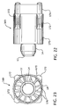
- Figures 22 and 23 show a side view and a front view, respectively, of one embodiment of a light source assembly 169 according to the present invention.
- the light source assembly 169 includes the lens 12, the lens holder 14, the first heat sink 16, the second heat sink 18, a housing 170, one or more standoffs 172, and a fan assembly 174 including fan blades 176.
- the housing 170 extends about the first heat sink 16 and the second heat sink 18 and is in coaxial relation therewith.
- the lens holder 14 has an end portion received into the housing 170.
- Embodiments of the present invention described above may be used in a variety of applications requiring optical radiation, such as activating tooth-whitening materials.
- a tooth whitening material is first applied to the teeth.
- the teeth are then exposed to the material in the absence of activating light for a substantial period of time.
- the material is then exposed to light having a wavelength in the range 400-600 nm.
- the light is generated by the light source 52,112 portion of the illuminator assembly 10 and is emitted forwardly toward the concave wall or recess 22 defined by the lens 12 and emerges from the light exit end 24 of the lens 12.
- the activating light may be applied to the material at a power level of 100-600 mW for a period of 20-40 seconds, for example.
- a dental composite material may be applied to a tooth and utilizing the light source 52,112 comprising an array of LEDs 93,120, 122,124 to produce activating light having a wavelength in the range 400-600 for example, the material may be cured.
- the light may be emitted forwardly from the light source 52,112 toward a concave wall forming the recess 22 defined by the lens 12 at the light entrance end 20.
- the activating light may be applied to the dental material at a power level of 100-200 mW for a period of seconds, for example.
- the dental composite material may be a resin applied to a tooth.
Abstract
Description
- The present invention relates generally and in various embodiments to illuminator assemblies. More specifically, the present invention relates generally and in various embodiments to illuminator assemblies including heat sinks.
- Although various implementations of the present invention, among many, may be described herein with reference to the specific illustrative embodiments, those skilled in the art will understand that the invention is not in any way intended to be, nor should be, limited to such embodiments. Those having ordinary skill in the art and reference to the description of the embodiments disclosed and described herein will recognize that additional modifications, and other embodiments may fall within the scope of the claimed invention, and that there may be additional fields in which the present invention may be used.
- Compact sources of light are needed for a variety of applications in dentistry and surgery such as surgical cutting, curing of dental composite materials, and activating tooth-whitening materials, for example. Furthermore, dentists may use high intensity light for correcting diseases or defects in hard tissues such as the enamel and dentin portions of the teeth where drills are normally used. In other applications, for example, dentists may use high intensity light for curing a variety of resins and composites in a patient's mouth and for bleaching teeth. Dental composite curing and teeth bleaching application generally require sources of light that emit light having wavelengths in the ultra violet (UV) portion of the spectrum. Surgeons may use high power/high intensity sources of light in certain applications for correcting diseases or defects in soft tissues for which scalpels and other similar surgical cutting instruments are normally used. Cutting applications also may require sources of light that emit light having wavelengths in various portions of the spectrum.
- Working in small confined areas such as a patient's mouth, for example, requires that the source of light be compact in size and highly maneuverable. Recent advances in solid state semiconductor technology in the field of laser diodes and light emitting diodes (LEDs) have enabled the miniaturization of these sources of light. Although compact in size, these solid state sources of light generally do not generate an adequate amount of power for the applications described above. When conventional solid state sources of light are driven with higher electrical input power to generate higher optical output power, thermal management becomes difficult and is an important obstacle to overcome in order to provide a source of light having enough intensity in optical output power to make it useful for certain dental and surgical applications, and other fields that may require a high intensity source of light for working in confined areas.
-
US2002/0113244A1 describes a high power illumination assembly comprising an LED package. The LED is located on a large cathode which acts as a heat sink, conducting heat away from the LED. The cathode sits within a lead frame comprising an annular anode and a liquid crystal polymer, which provides for thermal conduction whilst electrically insulating the anode from the cathode. Finally, a dome-shaped lens is seated over the lead frame, providing protection for the LED package as well as collecting and shaping light emitted by the LED. - The present invention is directed to an apparatus, as recited in claim 1, that includes a lens having a light entrance end forming a recess, a heat sink having an end portion facing the recess, and a light source positioned to transmit light via the recess into the lens in thermal communication with the heat sink, wherein heat generated by the light source is conducted to the heat sink. The lens is a non-imaging lens, such as a total internal reflection (TIR) lens, and has a rearward portion defining an outer surface which tapers to a smaller diameter in the direction of the heat sink. The lens holder has a front portion for receiving the lens with a tapered inner surface to accommodate it. The lens holder also has a rear portion for receiving an end portion of the heat sink on which the light source is mounted.
- In this manner the illuminator assembly of the present invention provides an alternative compact light source to those known in the art.
- Embodiments of the present invention are described herein in conjunction with the following figures, wherein:
- Figure 1 is a sectioned assembly view of one embodiment of an illuminator assembly;
- Figures 2 and 3 are side and end views, respectively, of one embodiment of a lens;
- Figures 4, 5, and 6 are side, end, and sectioned views, respectively, of one embodiment of a lens holder;
- Figures 7 and 8 are sectioned and end views, respectively, of one embodiment of a heat sink;
- Figures 9 and 10 are side and end views, respectively, of one embodiment of a heat sink, Figure 9 showing wiring to LEDs, which are also shown in Figure 10;
- Figures 11 and 12 are sectioned and end views, respectively, of one embodiment of a secondary heat sink;
- Figure 13 is a sectioned view of one embodiment of the heat sink shown in Figures 11 and 12;
- Figure 14 is an end view of one embodiment of the heat sink shown in Figures 11, 12, and 13;
- Figures 15 and 16 show one embodiment of a terminal board;
- Figure 17 is an end view of one embodiment of a light source assembly showing an LED array wiring configuration;
- Figure 18 is an end view of another embodiment of a light source assembly showing an LED array wiring configuration;
- Figures 19, 20, and 21 show an end view, a sectioned view, and a side view, respectively, of another embodiment of a terminal board; and
- Figures 22 and 23 show a side view and an end view, respectively, of one embodiment of an illuminator assembly.
- It is to be understood that the figures and descriptions of the various embodiments of present invention described herein, among others, have been simplified to illustrate representative elements of various embodiments of illuminator assemblies comprising various embodiments of light source assemblies that may be used in a variety of applications, such as, for example, applications requiring the use of high intensity light when working in confined quarters. The representative elements described herein are relevant for a clear understanding of the present invention. For purposes of clarity, however, other specific elements that would not facilitate a better or clearer understanding of the present invention may not be described herein. Those of ordinary skill in the art will appreciate, however, that these and other elements may be found in conventional illuminator assemblies and may be readily understood.
- Figure 1 is a sectioned assembly view of one embodiment of an
illuminator assembly 10 in accordance with the present invention. Theilluminator assembly 10 may comprise a variety of components such as alens 12, alens holder 14, afirst heat sink 16, and, optionally, asecond heat sink 18, for example. Theheat sink lens 12 and thefirst heat sink 16 may be coaxially aligned. In one embodiment of the present invention, thefirst heat sink 16 and thelens holder 14 also may be coaxially aligned. In one embodiment of the present invention, theilluminator assembly 10 may include a housing 170 (e.g., see Figures 22, 23) extending about thefirst heat sink 16 and is in coaxial relation therewith. Further, thelens holder 14 may include an end portion that is received into thehousing 170. Also, in one embodiment of the present invention, thefirst heat sink 16 may act as a primary heat sink for conducting heat away from the light source while thesecond heat sink 18 may act as a secondary heat sink for conducting heat away from thefirst heat sink 16. - With reference to the embodiments depicted in Figures 1-23, the
lens 12 may include, for example, alight entrance end 20 forming arecess 22 and alight exit end 24 where light generated by a light source assembly 50 (e.g., see Figures 9, 10, 17) located on anend portion 30 of thefirst heat sink 16 is emitted. Thelens 12 also may include a forwardcylindrical portion 25 and arearward portion 26 extending about therecess 22 that defines anouter surface 28 that tapers in adirection 27 toward thefirst heat sink 16 and/or thesecond heat sink 18. - The
lens holder 14 may include afront portion 32 that extends about therecess 22 of thelens 12 and may include arear portion 34 for receiving theend portion 30 of thefirst heat sink 16. Thus theend portion 30 of the first heat sink 16 projects endwise into thelens holder 14. Thelens holder 14 also may define aninner wall 35 that tapers in adirection 27 toward thefirst heat sink 16 and/or thesecond heat sink 18. The lens's taperingouter surface 28 also may extend into the tapered portion of the lens holder'sinner wall 35. The lens'souter surface 28 also tapers in thedirection 27 toward thefirst heat sink 16 and/or thesecond heat sink 18 and is oriented in adjacent relation to the lens holder's 14inner wall 35. - The
illuminator assembly 10 in accordance with one embodiment of the present invention also may include a first current carryingwire 36 that extends between thelens holder 14 and thefirst heat sink 16 and/or thesecond heat sink 18. The first current carryingwire 36 may be used to supply electrical current to the light source. The first current carryingwire 36 may be received in anopening 38 formed in thelens holder 14. - Figures 2 and 3 show a side view and an end view A-A, respectively, of one embodiment of the
lens 12 component of theilluminator assembly 10 according to the present invention. As discussed previously, thelens 12 may include, for example, thelight entrance end 20 forming therecess 22 and thelight exit end 24 for emitting the light generated by thelight source assembly 50. As illustrated, thelens 12 has a forwardcylindrical portion 25 and a rearwardarcuate portion 26 that extends about therecess 22. Thearcuate portion 26 defines anouter surface 28 that tapers in thedirection 27 toward thefirst heat sink 16 and/or thesecond heat sink 18. In one embodiment of the present invention, therecess 22 may be re-entrant into thelens 12. Thelens 12 may include arearward wall 23 that is concave in adirection 21 toward therecess 22. In one embodiment of the present invention, therecess 22 may be filled with a light transmitting material, such as, for example, a light transmitting plastic material. For example, therecess 22 may contain an optical plastic material having a predetermined index of refraction. In one embodiment, the index of refraction of the optical plastic material may be substantially the same as the index of refraction as thelens 12 material. Further, the optical plastic material contained in therecess 22 may be curable by light having a wavelength in the ultra-violet (UV) portion of the optical spectrum, for example. Thelens 12, for example, may be a non-imaging lens and may be formed of a variety of materials such as optical polycarbonate, for example. In one embodiment of the present invention, thelens 12 may be a total internal reflection (TIR) lens. - Figures 4, 5, and 6 are side, end, and sectioned views, respectively, of one embodiment of the
lens holder 14 component of theilluminator assembly 10 according to the present invention. Thefront portion 32 of thelens holder 14 defines afirst cavity 33 for receiving thelight entrance end 20 of thelens 12. Thefront portion 32 and theinner wall 35 of thelens holder 14 extend about therecess 22 of thelens 12. Therear portion 34 of thelens holder 14 defines asecond cavity 37 for receiving theend portion 30 of thefirst heat sink 16 such that theend portion 30 of thefirst heat sink 16 including thelight source assembly 50 projects endwise into thelens holder 14. Theinner wall 35 of thelens holder 14 tapers to a smaller diameter in thedirection 27 toward thefirst heat sink 16 and/or thesecond heat sink 18. The taperingouter surface 28 of thelens 12 extends into the taperedinner wall 25 portion of thelens holder 14. Theouter surface 28 of thelens 12 is in adjacent relation to theinner wall 35 of thelens holder 14 and is tapered toward thefirst heat sink 16 and/or thesecond heat sink 18. Thelens holder 14 also defines anopening 38 for receiving the firstcurrent carrying wire 36 therethrough. In one embodiment of the present invention, thelens holder 14 may be formed of Teflon, for example. - Figures 7 and 8 are side and end views, respectively, of one embodiment of the
first heat sink 16 component, according to the present invention, where Figure 7 is a sectioned view. Thefirst heat sink 16 comprises abody portion 40, which may include anend portion 30 that faces therecess 22 portion of thelens 12. Theend portion 30 is received into thesecond cavity 37 defined by therear portion 34 of thelens holder 14. Theend portion 30 also includes aface portion 31 for receiving the light source assembly 50 (e.g., see Figures 9 and 10). In one embodiment of the present invention, theface portion 31 of thefirst heat sink 16 may be gold plated and/or gold/nickel plated such that theface portion 31 is rendered suitable for attaching a semiconductor die or chip directly thereon and is rendered suitable for accepting wire bonds thereon. For thermal management purposes, thelight source assembly 50 is placed in thermal communication or in contact with thebody portion 40 orend portion 30 of thefirst heat sink 16 and/or with thesecond heat sink 18. Thus, thefirst heat sink 16 acts a thermal conductor and itsbody portion 40 conducts heat away from thelight source assembly 50. Thebody portion 40 of thefirst heat sink 16 also may transmit heat generated by thelight source assembly 50 to thesecond heat sink 18 formed about thefirst heat sink 16. Thebody portion 40 of thefirst heat sink 16 also may include achannel 42 formed therein for receiving the firstcurrent carrying wire 36 so that electrical current may be supplied to thelight source assembly 50 located on theface portion 31 of thefirst heat sink 16. Thebody portion 40 of thefirst heat sink 16 also may include anelongated portion 44, which may define ahollow portion 46 for receiving a second wire 48 (e.g., see Figure 9) therein. - The
body portion 40 of thefirst heat sink 16 may be formed of a variety of materials that are thermally conductive and/or electrically conductive materials such as, for example, aluminum, brass, bronze, copper, gold, nickel, platinum, steel, and the like, and/or any combinations of such materials including plated forms of such materials. In one embodiment, thefirst heat sink 16 may be nickel or gold plated copper. In one embodiment of the present invention, thefirst heat sink 16 may be nickel or gold plated on portions of thebody 40 to make electrical connections. In other embodiments, thefirst heat sink 16 and thesecond heat sink 18 may be integrally formed. - Figures 9 and 10 are also side and end views, respectively, of one embodiment of the
first heat sink 16 component according to the present invention. Thefirst heat sink 16 is shown wired to one embodiment of alight source assembly 50 according to the present invention. Thelight source assembly 50, may comprise, for example, alight source 52 including a plurality or array of light emitting diodes 93 (LEDs) in semiconductor die form, and may be arranged in a predetermined manner as shown. Thelight source assembly 50 is located on theface portion 31 of thefirst heat sink 16. Thelight source assembly 50 is positioned such that it faces therecess 22 formed on thelight entrance portion 20 of thelens 12. Accordingly, the light emitted from thelight source 52 is transmitted via therecess 22 and the material contained in therecess 22. In one embodiment of the present invention, thelight source assembly 50 may comprise one or more LED semiconductor die(s) 93 die bonded to theface portion 31 of theend portion 30 of thefirst heat sink 16. Thelight source assembly 50 also may include aninterface board 56 for making an appropriate physical electrical connection between a light source power supply and thelight source 52. At one end, thefirst wire 36 is electrically connected to theinterface board 56 atsolder connection 58. At another end, thefirst wire 36 is connected to a light source power supply. For example, thefirst wire 36 may supply electrical current to thelight source 52 or may provide a return path (e.g., ground) for thelight source 52. Theinterface board 56 also may serve for receiving wire bonds, e.g., from the LED semiconductor dies 93. - A
second wire 48 may be electrically attached to theelongated portion 44 of thefirst heat sink 16 by any well known means of attachment, such as asolder connection 54, a weld, screw, and the like. Thesecond wire 48 also may be attached directly to an outer wall of the body portion as shown in Figure 9. In one embodiment of the present invention, thebody portion 40 of thefirst heat sink 16 may be connected to an electrical connection of thelight source assembly 50 through thesecond wire 48. The electrical connection may be used to supply power or a return path (e.g., ground) through thesecond wire 48. Those skilled in the art will appreciate, however, that thesecond wire 48 may be used as return signal or ground wire, without departing from the scope of the present invention. - The
light source 52 may be coated with an optically transmissive encapsulatingmaterial 60, such as UV curable adhesive optical acrylic material, for example. In one embodiment of the present invention, the encapsulatingmaterial 60 is placed in a mold such that its shape conforms to the surface contour of therecess 22 formed in thelight entrance end 20 of thelens 12. Conforming the shape of the encapsulatingmaterial 60 to the contour of therecess 22 helps to transmit the light generated by thelight source 52 to thelens 12 and through thelight exit end 24 of thelens 12. Thelight source assembly 50 will be discussed below in more detail with respect to Figures 15-21. - Figures 11 and 12 are sectioned and end views, respectively, of one embodiment the
second heat sink 18 component of theilluminator assembly 10 according to the present invention. Figure 13 is a sectioned view of thesecond heat sink 18 component and Figure 14 is an end view thereof. Thesecond heat sink 18 includes abody 62 having a plurality offins 64 for conducting heat away from thefirst heat sink 16. The secondaryheat sink body 62 defines anopening 66 for receiving thesecond wire 48 therethrough. The secondaryheat sink body 62 also may define a passage orchannel 68 for receiving thefirst wire 36 therethrough. Thebody 62 may be formed of a plurality of thermally conductive materials such as, for example, aluminum, brass, bronze, copper, gold, nickel, platinum, steel, and the like, and/or any combinations of such materials including plated forms of such materials. The materials may be the same or different form thefirst heat sink 16. - Figures 15 and 16 show a top view and sectioned view, respectively, of one embodiment of the
interface board 56 according to the present invention. Theinterface board 56 may comprise, for example, asubstrate 57, which may be in the form of a ring defining an aperture or may have a shape that conforms to theface portion 31 of thefirst heat sink 16. Thesubstrate 57 may include, for example, aninner wall 70 and anouter wall 72. Thesubstrate 57 may have athickness 82 of about 0.025 inches, for example. - In one embodiment of the present invention, the
substrate 57 may be formed of ceramic or any other material suitable for depositing metallic films thereon, such as for example, alumina, glass, silicon or other semiconductor, aluminum, copper, gold, silver, nickel, and the like. In one embodiment of the present invention, thesubstrate 57 may include a first metallicconductive film 74 processed on atop surface 76 thereof. In one embodiment of the present invention thefilm 74 may be a thin film of gold, or other metal, suitable for wire bonding thereto, for example. Thefilm thickness 80 may range, for example, from about 5 to about 10 microns. In one embodiment of the present invention, thetop surface 76 of thesubstrate 57 may include aconductive pad 78 having a second metallicconductive film 79 processed thereon suitable for making a solder, or other electrical connection, thereto. Thus theconductive pad 78 may form an electrical connection between thefirst wire 36 and theinterface board 56. The second metallicconductive film 79 may be, for example, a platinum silver paste having a thickness ranging from about 10 to about 16 microns, for example. The second metallicconductive film 78 may be suitable, for example, for attaching thefirst wire 36 to theinterface board 56 at asolder connection 58 for supplying electric current to thelight source 52, for example. The first and second metallicconductive films surface 76 of theinterface board 56 by any one of a plurality of well known methods for processing such films, such as, for example, sputtering, vacuum deposition, screen printing and firing, and the like. - Figure 17 is an end view of one embodiment of the
light source assembly 50, shown in greater detail, including a nine up wiring configuration of theLED array 52. TheLED array 52 comprises a plurality of LEDs semiconductor dies 93 die bonded to theface portion 31 of thefirst heat sink 16, for example. As discussed previously, theface portion 31 may provide a return path or ground connection to the power supply for thelight source assembly 50. Theinterface board 56 also comprises themetallic conducting film 74 deposited on thesurface 76 thereof. Themetallic conducting film 76 may be chosen for wire bonding any suitable type of wire bonds, such as, for example, gold or aluminum wire bonds. The LED semiconductor dies 93 may be wire bonded to thetop surface 76 of theinterface board 56 viawire bonds 94, for example. Electric current may be supplied to the LED semiconductor dies 93 via the wire bonds 94. The LED semiconductor dies 93 may be interconnected to each other via wire bonds 96. The LED semiconductor dies 93 also may be connected to theface portion 31 of thefirst heat sink 16 viawire bonds 98, for example. As shown, theLED array 52 is formed of three banks ofLEDs conductive wire 36 may be connected to theinterface board 56 throughsolder connection 58 and may be used to supply electric current to thelight source assembly 50. Thesolder connection 58 may be formed, for example, over theconductive pad 78 through themetallic conducting film 79 deposited thereon. In one embodiment of the present invention themetallic conducting film 79 may be a palladium silver compound processed over theconductive pad 78, for example. - Figure 18 is an end view of another embodiment of a
light source assembly 110 comprising alight source 112 formed, for example, of one or more LED semiconductor dies 120, 122, 124. Thelight source 112 comprises a plurality ofLED banks face portion 31 of thefirst heat sink 16, for example. EachLED bank first LED bank 114 may comprise an LED semiconductor die 120 that emits red light having an intensity of up to about 700 lumen, for example. Thesecond LED bank 116 may comprise an LED semiconductor die 122 that emits blue light having an intensity of up to 100 about lumen, for example. Thethird LED bank 118 may comprise an LED semiconductor die 124 that emits green light having an intensity of up to about 100 lumen. Those skilled in the art will appreciate, however, that embodiments of the present invention is not limited to these wavelengths and may include any combination of LED semiconductor dies 120, 122, 124 that emit light of any wavelength without departing from the scope of the present invention, including for example, LED semiconductor dies that emit amber light having an intensity of up to about 70 lumen. - As discussed previously the
face portion 31 of thefirst heat sink 16 provides one of the electrical connections to thelight source assembly 110. For example, in one embodiment of the present invention, theface portion 31 may provide a ground connection or electric current return path to a light source power supply, for example. Thelight source assembly 110 also may comprise aninterface board 126 including a plurality of individual wire bondableconductive pads conductive pad metallic conducting film 74 deposited on the surface thereof, for example, and theconductive film 74 is suitable for wire bonding the LED semiconductor dies 120, 122, 124 to theinterface board 126. In one embodiment of the present invention, the three individualconductive pads face portion 31 of the first heat sink. - Electrical current may be separately supplied and separately controlled to each
LED bank wires wire conductive pad solder connections LED bank LED bank LED bank - The individual LED semiconductor dies 120, 122, 124 forming any one of the
LED banks first LED bank 114 may be connected to theconductive pad 128 via wire bonds 148. Similarly, second andthird LED banks conductive pads wire bonds LED bank face portion 31 of the first heat sink throughwire bonds 154. - Figures 19, 20, and 21 show a top view, sectioned view, and side view, respectively, of another embodiment of an
interface board 155 according to the present invention. In one embodiment of the present invention, theinterface board 155 comprises asubstrate 157 in the form of a ring having aninner wall 156 and anouter wall 158. In one embodiment of the present invention, thesubstrate 157 may be formed of ceramic or any other material suitable for depositing metallic films thereon, such as for example, alumina, glass, silicon or other semiconductor, aluminum, copper, gold, silver, nickel, and the like. Thesubstrate 157thickness 160 may be about 0.04 inches, for example. - In one embodiment of the present invention, the interface board's 155
substrate 157 may include a first metallicconductive film 162 processed on atop surface 164 thereof. In one embodiment of the present invention thefilm 162 may be a thin film of gold, or any other metal, suitable for wire bonding, for example. Thefilm thickness 164 may be any thickness that provides sufficient electrical conductivity, such as, a range from about 5 to about 10 microns, for example. In one embodiment of the present invention, thetop surface 164 of thesubstrate 157 also may include aconductive pad 166 having a second metallicconductive film 168 processed thereon suitable for forming an electrical connection between any of the wires 36,134, 136,138 and theinterface board 155 through the various solder connections 58,140, 142,144. The second metallicconductive film 168 may be, for example, a palladium silver paste having a thickness ranging from about 10 to about 16 microns, for example. The second metallicconductive film 168 may be suitable, for example, for attaching any of the wires 36,134, 136,138 to theinterface board 155 to provide electric current to thelight source assembly 110. The first and second metallic conductive films 162,166 may be processed onto thesurface 164 of theinterface board 155 using any one of a plurality of well known methods for processing such films, such as, for example, sputtering, vacuum deposition, screen printing and firing, and the like. - Figures 22 and 23 show a side view and a front view, respectively, of one embodiment of a
light source assembly 169 according to the present invention. Thelight source assembly 169 includes thelens 12, thelens holder 14, thefirst heat sink 16, thesecond heat sink 18, ahousing 170, one ormore standoffs 172, and afan assembly 174 includingfan blades 176. Thehousing 170 extends about thefirst heat sink 16 and thesecond heat sink 18 and is in coaxial relation therewith. Thelens holder 14 has an end portion received into thehousing 170. - Embodiments of the present invention described above may be used in a variety of applications requiring optical radiation, such as activating tooth-whitening materials. For example, to whiten teeth, a tooth whitening material is first applied to the teeth. The teeth are then exposed to the material in the absence of activating light for a substantial period of time. The material is then exposed to light having a wavelength in the range 400-600 nm. The light is generated by the light source 52,112 portion of the
illuminator assembly 10 and is emitted forwardly toward the concave wall orrecess 22 defined by thelens 12 and emerges from thelight exit end 24 of thelens 12. The activating light may be applied to the material at a power level of 100-600 mW for a period of 20-40 seconds, for example. - Moreover, embodiments of the present invention may be used to cure dental composite materials. For example, a dental composite material may be applied to a tooth and utilizing the light source 52,112 comprising an array of LEDs 93,120, 122,124 to produce activating light having a wavelength in the range 400-600 for example, the material may be cured. The light may be emitted forwardly from the light source 52,112 toward a concave wall forming the
recess 22 defined by thelens 12 at thelight entrance end 20. The activating light may be applied to the dental material at a power level of 100-200 mW for a period of seconds, for example. The dental composite material may be a resin applied to a tooth. - Although the present invention has been described with regard to certain embodiments, those of ordinary skill in the art will recognize that many modifications and variations of the present invention may be implemented. The foregoing description and the following claims are intended to cover all such modifications and variations. Furthermore, the components disclosed are illustrative, but are not exhaustive. Other components also may be used to make systems embodying the present invention.
Claims (24)
- A compact illuminator assembly (10) comprising:a lens (12) having a light entrance end (20) forming a recess (22) and a rearward portion (26) extending about the lens recess (22), the lens (12) being configured to radiate optical radiation therethrough;a heat sink (16) having an end portion (30) facing the lens recess (22);a lens holder (14) including a rear portion (34) defining a second cavity (37) for receiving the end portion (30) of the heat sink (16) therein; and,a light source (52) positioned on the end portion (30) of the heat sink (16) facing the light entrance end (20) of the lens (12) to transmit light via the lens recess (22) into the lens, the light source (52) being in thermal communication with the heat sink (16) wherein heat generated by the light source (52) is conducted to the heat sink (16),characterized in that the lens holder (14) includes a front portion (32) extending about the lens recess (22), the front portion (32) defining a first cavity (33) for receiving the light entrance end (20) of the lens (12), the lens holder (14) defining an inner wall (35) therein tapering to a smaller diameter in a direction (27) from the front portion (32) of the lens holder (14) to the rear portion (34) of the lens holder (14),
and further characterized in that the lens (12) is a non-imaging lens and that the rearward portion (26) of the lens (12) defines an outer surface (28) tapering to a smaller diameter in the direction (27) of the heat sink (16), the tapered outer surface (28) of the lens (12) further extending into the rear portion (34) of the lens holder (14) and the tapered outer surface (28) of the lens (12) being oriented in adjacent relation to the tapered inner wall (35) of the lens holder (14). - The illuminator assembly (10) of Claim 1, wherein the heat sink (16) further comprises a metallic film formed on a surface (31) thereof.
- The illuminator assembly (10) of Claim 2, wherein the metallic film is formed on the end portion (30) of the heat sink (16) facing the recess (22).
- The illuminator assembly (10) of Claim 2, wherein the light source (52) is attached to the metallic film formed on the end portion of the heat sink.
- The illuminator assembly (10) of Claim 1, wherein the light source (52) comprises an LED (93).
- The illuminator assembly (10) of Claim 1, wherein the light source (52) comprises a plurality of LEDs (93).
- The illuminator assembly (10) of Claim 1, further comprising an annular interface board (56) located on the end portion (30) of the heat sink (16), the light source (52) being positioned in a central aperture defined by the annular interface board (56).
- The illuminator assembly (10) of Claim 7, further comprising a metallic film (74) formed on the interface board (56), wherein the light source (52) is electrically connected to the metallic film (74) formed on the interface board (56).
- The illuminator assembly (10) of Claim 7, wherein the interface board (56) comprises a conductive pad (78) formed on a surface (76) thereof, and wherein electrical current is supplied to the light source (52) through the interface board (56) via the conductive pad (78).
- The illuminator assembly (10, 110) of Claim 7, wherein the interface board (126) comprises a plurality of conductive pads (128, 130, 132) formed on a surface thereof.
- The illuminator assembly (10, 110) of Claim 10, wherein the interface board (126) comprises three conductive pads (128, 130, 132) spaced 120° apart.
- The illuminator assembly (10) of Claim 1, wherein the heat sink (16) forms an electrical contact of the light source (52).
- The illuminator assembly (10) of Claim 1, wherein the light source (52) is configured to emit light having a predetermined visible wavelength forwardly toward the lens recess (22).
- The illuminator assembly (10) of Claim 1, wherein the lens recess (52) is re-entrant into the lens (12), and the lens includes a rearward wall (23) that is concave toward the lens recess (22).
- The illuminator assembly (10) of Claim 1, wherein the lens recess (22) contains at least one of the following:i) a curable optical plastic material having an index of refraction substantially the same as that of the lens; orii) a light transmitting plastic material.
- The illuminator assembly (10) of Claim 1, wherein the light source (52) is in thermal communication with the end portion (30) of the heat sink (16).
- The illuminator assembly (10) of Claim 1, wherein the lens (12) and the heat sink (16) are coaxially aligned.
- The illuminator assembly (10) of Claim 1, wherein the heat sink (16) comprises a body (40) that projects endwise into the lens holder (14).
- The illuminator assembly (10) of Claim 1, further comprising wiring (36) extending between the lens holder (14) and the heat sink (16) to supply electrical current to the light source (52) which comprises an LED (43) or an array of LEDs (43).
- The illuminator assembly (10) of Claim 1, wherein the lens (12), the heat sink (16), and the lens holder(14) are coaxially aligned.
- The illuminator assembly (10) of Claim 1, further comprising a light transmitting member (60) transmitting light from the lens (12) in a direction away from the recess (22).
- The illuminator assembly (10, 169) of Claim 1, further comprising a housing (170) extending about the heat sink (16) in coaxial relation therewith, the lens holder (14) having an end portion received into the housing (170).
- The illuminator assembly (10) of Claim 1, wherein the heat sink (16) is a primary heat sink (16), and there being a secondary heat sink (18) in thermal communication with the primary heat sink (16).
- The illuminator assembly (10) of claim 1, wherein the non-imaging lens (12) is a total internal reflection (TIR) lens.
Applications Claiming Priority (3)
| Application Number | Priority Date | Filing Date | Title |
|---|---|---|---|
| US41444302P | 2002-09-30 | 2002-09-30 | |
| US414443P | 2002-09-30 | ||
| PCT/US2003/030696 WO2004032254A1 (en) | 2002-09-30 | 2003-09-30 | Illuminator assembly |
Publications (2)
| Publication Number | Publication Date |
|---|---|
| EP1550167A1 EP1550167A1 (en) | 2005-07-06 |
| EP1550167B1 true EP1550167B1 (en) | 2007-11-28 |
Family
ID=32069737
Family Applications (1)
| Application Number | Title | Priority Date | Filing Date |
|---|---|---|---|
| EP03752632A Expired - Lifetime EP1550167B1 (en) | 2002-09-30 | 2003-09-30 | Illuminator assembly |
Country Status (7)
| Country | Link |
|---|---|
| US (2) | US7163318B2 (en) |
| EP (1) | EP1550167B1 (en) |
| JP (1) | JP2006504253A (en) |
| AU (1) | AU2003270918A1 (en) |
| CA (1) | CA2500479C (en) |
| DE (1) | DE60317808T2 (en) |
| WO (1) | WO2004032254A1 (en) |
Families Citing this family (108)
| Publication number | Priority date | Publication date | Assignee | Title |
|---|---|---|---|---|
| US6200134B1 (en) | 1998-01-20 | 2001-03-13 | Kerr Corporation | Apparatus and method for curing materials with radiation |
| CA2500479C (en) * | 2002-09-30 | 2012-11-06 | Teledyne Lighting And Display Products, Inc. | Illuminator assembly |
| US7147468B2 (en) | 2002-12-31 | 2006-12-12 | Water Pik, Inc. | Hand held oral irrigator |
| US20050286845A1 (en) * | 2004-06-17 | 2005-12-29 | Plocharczyk John R | Fiberoptic device for dental or industrial use |
| WO2006083228A1 (en) * | 2005-02-07 | 2006-08-10 | Amdent Ab | Dental handpiece |
| DE602005024315D1 (en) * | 2005-03-31 | 2010-12-02 | Neobulb Technologies Inc | HIGH-PERFORMANCE LED LIGHTING DEVICE WITH HIGH THERMAL DIFFUSION CAPACITY |
| US20080268401A1 (en) * | 2005-04-08 | 2008-10-30 | Invisitech Co., Ltd. | Led Having Wide Wavelength-Range and Light Curing Unit Using the Same |
| US8459852B2 (en) | 2007-10-05 | 2013-06-11 | Dental Equipment, Llc | LED-based dental exam lamp |
| US7918591B2 (en) * | 2005-05-13 | 2011-04-05 | Permlight Products, Inc. | LED-based luminaire |
| US20070203439A1 (en) | 2006-02-24 | 2007-08-30 | Water Pik, Inc. | Water jet unit and handle |
| JP4577846B2 (en) * | 2006-02-28 | 2010-11-10 | スタンレー電気株式会社 | Lighting device |
| US7670141B2 (en) | 2006-07-07 | 2010-03-02 | Water Pik, Inc. | Oral irrigator |
| USD802120S1 (en) | 2007-02-27 | 2017-11-07 | Water Pik, Inc. | Tip for oral irrigator |
| TWI340219B (en) * | 2008-05-09 | 2011-04-11 | Neobulb Technologies Inc | Outdoor illuminating apparatus |
| BRPI0804147B8 (en) * | 2008-09-25 | 2021-06-22 | Jose Humberto Yatsuda Moromizato | improvements introduced in cutaneous transilluminator apparatus |
| DE102008054196A1 (en) * | 2008-10-31 | 2010-05-06 | Sycotec Gmbh & Co. Kg | Light emitting device and drive device with a light emitting diode |
| BRPI0923789B8 (en) * | 2008-12-30 | 2021-06-22 | Ultradent Products Inc | dental healing light having unique body design that acts as a heat sink |
| US10258442B2 (en) | 2009-03-20 | 2019-04-16 | Water Pik, Inc. | Oral irrigator appliance with radiant energy delivery for bactericidal effect |
| JP5643284B2 (en) * | 2009-03-20 | 2014-12-17 | ウォーターピック,インコーポレイティド | Oral irrigator with bactericidal action by radiant energy delivery |
| US9072572B2 (en) | 2009-04-02 | 2015-07-07 | Kerr Corporation | Dental light device |
| US9066777B2 (en) | 2009-04-02 | 2015-06-30 | Kerr Corporation | Curing light device |
| DE102009038827B4 (en) * | 2009-08-25 | 2012-10-25 | Heine Optotechnik Gmbh & Co Kg | Led lamp |
| US9581756B2 (en) | 2009-10-05 | 2017-02-28 | Lighting Science Group Corporation | Light guide for low profile luminaire |
| US9028091B2 (en) | 2009-10-05 | 2015-05-12 | Lighting Science Group Corporation | Low profile light having elongated reflector and associated methods |
| US9157581B2 (en) | 2009-10-05 | 2015-10-13 | Lighting Science Group Corporation | Low profile luminaire with light guide and associated systems and methods |
| US8864340B2 (en) | 2009-10-05 | 2014-10-21 | Lighting Science Group Corporation | Low profile light having concave reflector and associated methods |
| DE102010012423A1 (en) * | 2009-12-21 | 2011-06-22 | OSRAM Opto Semiconductors GmbH, 93055 | Luminescence diode arrangement, backlighting device and display device |
| US8729581B2 (en) | 2010-01-13 | 2014-05-20 | Apple Inc. | Light guide for LED source |
| US10064698B2 (en) * | 2010-05-26 | 2018-09-04 | Zhengzhou Zezheng Technical Services Ltd. | Dental drill head |
| US9642687B2 (en) | 2010-06-15 | 2017-05-09 | The Procter & Gamble Company | Methods for whitening teeth |
| US9827439B2 (en) | 2010-07-23 | 2017-11-28 | Biological Illumination, Llc | System for dynamically adjusting circadian rhythm responsive to scheduled events and associated methods |
| US9532423B2 (en) | 2010-07-23 | 2016-12-27 | Lighting Science Group Corporation | System and methods for operating a lighting device |
| US8465167B2 (en) | 2011-09-16 | 2013-06-18 | Lighting Science Group Corporation | Color conversion occlusion and associated methods |
| US8760370B2 (en) | 2011-05-15 | 2014-06-24 | Lighting Science Group Corporation | System for generating non-homogenous light and associated methods |
| US8686641B2 (en) | 2011-12-05 | 2014-04-01 | Biological Illumination, Llc | Tunable LED lamp for producing biologically-adjusted light |
| US9024536B2 (en) | 2011-12-05 | 2015-05-05 | Biological Illumination, Llc | Tunable LED lamp for producing biologically-adjusted light and associated methods |
| US8841864B2 (en) | 2011-12-05 | 2014-09-23 | Biological Illumination, Llc | Tunable LED lamp for producing biologically-adjusted light |
| US9151482B2 (en) | 2011-05-13 | 2015-10-06 | Lighting Science Group Corporation | Sealed electrical device with cooling system |
| US9360202B2 (en) | 2011-05-13 | 2016-06-07 | Lighting Science Group Corporation | System for actively cooling an LED filament and associated methods |
| RU2573630C9 (en) * | 2011-10-12 | 2016-07-10 | Чжэнчжоу Цзэчжэн Текникал Сервисиз Лтд. | Head of dental drill |
| US9289574B2 (en) | 2011-12-05 | 2016-03-22 | Biological Illumination, Llc | Three-channel tuned LED lamp for producing biologically-adjusted light |
| US9220202B2 (en) | 2011-12-05 | 2015-12-29 | Biological Illumination, Llc | Lighting system to control the circadian rhythm of agricultural products and associated methods |
| US9913341B2 (en) | 2011-12-05 | 2018-03-06 | Biological Illumination, Llc | LED lamp for producing biologically-adjusted light including a cyan LED |
| US8963450B2 (en) | 2011-12-05 | 2015-02-24 | Biological Illumination, Llc | Adaptable biologically-adjusted indirect lighting device and associated methods |
| US9328898B1 (en) | 2012-02-21 | 2016-05-03 | Richard Arthur Flasck | High efficiency hybrid illumination system |
| JP6019730B2 (en) * | 2012-05-14 | 2016-11-02 | オムロン株式会社 | Ultraviolet irradiation device and ultraviolet irradiation head |
| FI20125933A (en) * | 2012-09-08 | 2014-03-09 | Lumichip Ltd | LED chip-on-board component and lighting module |
| US9127818B2 (en) | 2012-10-03 | 2015-09-08 | Lighting Science Group Corporation | Elongated LED luminaire and associated methods |
| WO2014059362A2 (en) | 2012-10-11 | 2014-04-17 | Water Pik, Inc. | Interdental cleaner using water supply |
| US9347655B2 (en) | 2013-03-11 | 2016-05-24 | Lighting Science Group Corporation | Rotatable lighting device |
| US9459397B2 (en) | 2013-03-12 | 2016-10-04 | Lighting Science Group Corporation | Edge lit lighting device |
| USD714929S1 (en) | 2013-03-14 | 2014-10-07 | Water Pik, Inc. | Base for water flosser |
| US9642677B2 (en) | 2013-03-14 | 2017-05-09 | Water Pik, Inc. | Oral irrigator with massage mode |
| CA3187593A1 (en) | 2013-03-15 | 2014-09-18 | Water Pik, Inc. | Brush tip with motion transfer and securing engagement structures |
| EP2842513A1 (en) * | 2013-08-28 | 2015-03-04 | W & H Dentalwerk Bürmoos GmbH | Lighting device for a medical, in particular dental instrument |
| US9429294B2 (en) | 2013-11-11 | 2016-08-30 | Lighting Science Group Corporation | System for directional control of light and associated methods |
| US9980793B2 (en) | 2013-11-27 | 2018-05-29 | Water Pik, Inc. | Oral hygiene system |
| EP3073956B1 (en) | 2013-11-27 | 2019-02-13 | Water Pik, Inc. | Oral irrigator with slide pause switch |
| CN203693808U (en) | 2013-12-12 | 2014-07-09 | 洁碧有限公司 | Dental water sprayer |
| KR20170058977A (en) | 2014-09-17 | 2017-05-29 | 개리슨 덴탈 솔루션즈, 엘엘씨 | Dental curing light |
| CN205586102U (en) | 2014-12-01 | 2016-09-21 | 洁碧有限公司 | Waterproof wireless oral cavity flusher |
| USD772396S1 (en) | 2014-12-01 | 2016-11-22 | Water Pik, Inc. | Handheld oral irrigator |
| USD780908S1 (en) | 2015-11-03 | 2017-03-07 | Water Pik, Inc. | Handheld oral irrigator |
| USD822196S1 (en) | 2016-01-14 | 2018-07-03 | Water Pik, Inc. | Oral irrigator |
| USD783809S1 (en) | 2016-01-25 | 2017-04-11 | Water Pik, Inc. | Oral irrigator handle |
| USD802747S1 (en) | 2016-07-19 | 2017-11-14 | Water Pik, Inc. | Reservoir for oral irrigator |
| USD786422S1 (en) | 2016-01-25 | 2017-05-09 | Water Pik, Inc. | Oral irrigator |
| CA3012050C (en) | 2016-01-25 | 2020-12-08 | Water Pik, Inc. | Reduced form factor oral irrigator |
| US10835356B2 (en) | 2016-01-25 | 2020-11-17 | Water Pik, Inc. | Swivel assembly for oral irrigator handle |
| USD804018S1 (en) | 2016-07-19 | 2017-11-28 | Water Pik, Inc. | Base for an oral irrigator |
| USD796028S1 (en) | 2016-07-19 | 2017-08-29 | Water Pik, Inc. | Oral irrigator |
| USD782656S1 (en) | 2016-01-25 | 2017-03-28 | Water Pik, Inc. | Oral irrigator |
| USD794773S1 (en) | 2016-07-19 | 2017-08-15 | Water Pik, Inc. | Oral irrigator |
| USD819956S1 (en) | 2016-01-25 | 2018-06-12 | Water Pik, Inc. | Kit bag |
| USD804016S1 (en) | 2016-02-05 | 2017-11-28 | Water Pik, Inc. | Handheld oral irrigator |
| USD783810S1 (en) | 2016-02-22 | 2017-04-11 | Water Pik, Inc. | Handle for an oral irrigator |
| USD809650S1 (en) | 2016-02-22 | 2018-02-06 | Water Pik, Inc. | Oral irrigator |
| USD802119S1 (en) | 2016-03-02 | 2017-11-07 | Water Pik, Inc. | Oral irrigator |
| CA3016031C (en) | 2016-03-02 | 2020-07-07 | Water Pik, Inc. | Actuation assembly for an oral irrigator |
| USD782657S1 (en) | 2016-03-02 | 2017-03-28 | Water Pik, Inc. | Oral irrigator handle |
| USD807822S1 (en) | 2016-07-19 | 2018-01-16 | Water Pik, Inc. | Power supply cartridge |
| USD809651S1 (en) | 2016-07-19 | 2018-02-06 | Water Pik, Inc. | Combination base and reservoir for an oral irrigator |
| USD840022S1 (en) | 2016-12-15 | 2019-02-05 | Water Pik, Inc. | Oral irrigator handle |
| US10779922B2 (en) | 2016-12-15 | 2020-09-22 | Water Pik, Inc. | Pause valve and swivel assemblies for oral irrigator handle |
| USD839409S1 (en) | 2016-12-15 | 2019-01-29 | Water Pik, Inc. | Oral irrigator unit |
| USD829886S1 (en) | 2016-12-15 | 2018-10-02 | Water Pik, Inc. | Oral irrigator base |
| USD832418S1 (en) | 2016-12-15 | 2018-10-30 | Water Pik, Inc. | Oral irrigator base |
| USD822825S1 (en) | 2016-12-15 | 2018-07-10 | Water Pik, Inc. | Oral irrigator unit |
| USD834180S1 (en) | 2016-12-15 | 2018-11-20 | Water Pik, Inc. | Oral irrigator base |
| USD833000S1 (en) | 2016-12-15 | 2018-11-06 | Water Pik, Inc. | Oral irrigator unit |
| USD825741S1 (en) | 2016-12-15 | 2018-08-14 | Water Pik, Inc. | Oral irrigator handle |
| USD832420S1 (en) | 2016-12-15 | 2018-10-30 | Water Pik, Inc. | Oral irrigator base |
| JP7146762B2 (en) | 2016-12-15 | 2022-10-04 | ウォーター ピック インコーポレイテッド | Oral irrigator with magnetic attachment |
| USD867579S1 (en) | 2016-12-15 | 2019-11-19 | Water Pik, Inc. | Oral irrigator unit |
| USD822826S1 (en) | 2016-12-15 | 2018-07-10 | Water Pik, Inc. | Oral irrigator base |
| USD833600S1 (en) | 2016-12-15 | 2018-11-13 | Water Pik, Inc. | Oral irrigator reservoir |
| USD840023S1 (en) | 2016-12-15 | 2019-02-05 | Water Pik, Inc. | Oral irrigator reservoir |
| USD832419S1 (en) | 2016-12-15 | 2018-10-30 | Water Pik, Inc. | Oral irrigator unit |
| USD810293S1 (en) | 2017-01-20 | 2018-02-13 | Garrison Dental Solutions, Llc | Dental instrument |
| USD833601S1 (en) | 2017-02-06 | 2018-11-13 | Water Pik, Inc. | Oral irrigator |
| USD833602S1 (en) | 2017-02-06 | 2018-11-13 | Water Pik, Inc. | Oral irrigator base |
| USD829887S1 (en) | 2017-02-06 | 2018-10-02 | Water Pik, Inc. | Oral irrigator reservoir |
| USD868243S1 (en) | 2018-03-16 | 2019-11-26 | Water Pik, Inc. | Oral irrigator tip |
| USD877324S1 (en) | 2018-05-17 | 2020-03-03 | Water Pik, Inc. | Oral irrigator handle |
| USD888936S1 (en) | 2019-02-22 | 2020-06-30 | Water Pik, Inc. | Cordless water flosser |
| USD889636S1 (en) | 2019-02-22 | 2020-07-07 | Water Pik, Inc. | Water flosser |
| USD966498S1 (en) | 2020-09-15 | 2022-10-11 | Water Pik, Inc. | Oral irrigator |
| USD1016274S1 (en) | 2021-02-16 | 2024-02-27 | Water Pik, Inc. | Oral irrigator |
Family Cites Families (28)
| Publication number | Priority date | Publication date | Assignee | Title |
|---|---|---|---|---|
| US4271408A (en) * | 1978-10-17 | 1981-06-02 | Stanley Electric Co., Ltd. | Colored-light emitting display |
| JPS5669607A (en) * | 1979-11-09 | 1981-06-11 | Mitsubishi Electric Corp | Photocoupler |
| EP0117606A1 (en) * | 1983-01-28 | 1984-09-05 | Xerox Corporation | Collector for a LED array |
| US5310344A (en) * | 1990-11-01 | 1994-05-10 | Arthur Vassiliadis | Dental laser system |
| US5401171A (en) * | 1992-07-20 | 1995-03-28 | Paghdiwala; Abid F. | Dental laser device and method |
| US5616141A (en) * | 1993-04-09 | 1997-04-01 | Ion Laser Technology | Laser system for use in dental procedures |
| IT1265106B1 (en) * | 1993-07-23 | 1996-10-30 | Solari Udine Spa | OPTICAL SYSTEM FOR LIGHT-EMITTING DIODES |
| WO1997001728A1 (en) * | 1995-06-29 | 1997-01-16 | Siemens Components, Inc. | Localized illumination using tir technology |
| US5752833A (en) * | 1996-04-19 | 1998-05-19 | Scalar Co. | Method for repairing dental enamel |
| GB2329756A (en) | 1997-09-25 | 1999-03-31 | Univ Bristol | Assemblies of light emitting diodes |
| US6200134B1 (en) * | 1998-01-20 | 2001-03-13 | Kerr Corporation | Apparatus and method for curing materials with radiation |
| US6077073A (en) | 1998-09-15 | 2000-06-20 | Jacob; Gregory S. | Light emitting diode-array light apparatus |
| US6439888B1 (en) | 1999-05-03 | 2002-08-27 | Pls Liquidating Llc | Optical source and method |
| US7086858B2 (en) * | 1999-09-24 | 2006-08-08 | Cao Group, Inc. | Semiconductor curing light system useful for curing light activated composite materials |
| US6719559B2 (en) * | 1999-09-24 | 2004-04-13 | Densen Cao | Curing light |
| US6331111B1 (en) * | 1999-09-24 | 2001-12-18 | Cao Group, Inc. | Curing light system useful for curing light activated composite materials |
| EP1891909B1 (en) * | 2000-08-04 | 2017-04-19 | Kerr Corporation | Apparatus for curing materials with light radiation |
| US6547423B2 (en) * | 2000-12-22 | 2003-04-15 | Koninklijke Phillips Electronics N.V. | LED collimation optics with improved performance and reduced size |
| US6639360B2 (en) * | 2001-01-31 | 2003-10-28 | Gentex Corporation | High power radiation emitter device and heat dissipating package for electronic components |
| US6541800B2 (en) * | 2001-02-22 | 2003-04-01 | Weldon Technologies, Inc. | High power LED |
| US20030076034A1 (en) * | 2001-10-22 | 2003-04-24 | Marshall Thomas M. | Led chip package with four led chips and intergrated optics for collimating and mixing the light |
| US6871983B2 (en) * | 2001-10-25 | 2005-03-29 | Tir Systems Ltd. | Solid state continuous sealed clean room light fixture |
| DE60111751T2 (en) * | 2001-11-22 | 2006-04-27 | Mectron S.R.L., Carasco | Optical system for a dental handpiece for the polymerization of light-curing materials or synthetic resins |
| US6832849B2 (en) * | 2001-12-04 | 2004-12-21 | Ccs, Inc. | Light radiation device, light source device, light radiation unit, and light connection mechanism |
| US6560038B1 (en) * | 2001-12-10 | 2003-05-06 | Teledyne Lighting And Display Products, Inc. | Light extraction from LEDs with light pipes |
| CA2500479C (en) * | 2002-09-30 | 2012-11-06 | Teledyne Lighting And Display Products, Inc. | Illuminator assembly |
| US6896381B2 (en) * | 2002-10-11 | 2005-05-24 | Light Prescriptions Innovators, Llc | Compact folded-optics illumination lens |
| US7029277B2 (en) * | 2002-10-17 | 2006-04-18 | Coltene / Whaledent Inc. | Curing light with engineered spectrum and power compressor guide |
-
2003
- 2003-09-30 CA CA2500479A patent/CA2500479C/en not_active Expired - Lifetime
- 2003-09-30 JP JP2004541842A patent/JP2006504253A/en active Pending
- 2003-09-30 WO PCT/US2003/030696 patent/WO2004032254A1/en active IP Right Grant
- 2003-09-30 AU AU2003270918A patent/AU2003270918A1/en not_active Abandoned
- 2003-09-30 DE DE60317808T patent/DE60317808T2/en not_active Expired - Lifetime
- 2003-09-30 EP EP03752632A patent/EP1550167B1/en not_active Expired - Lifetime
- 2003-09-30 US US10/675,504 patent/US7163318B2/en active Active
-
2006
- 2006-12-04 US US11/633,305 patent/US7344280B2/en not_active Expired - Lifetime
Also Published As
| Publication number | Publication date |
|---|---|
| CA2500479A1 (en) | 2004-04-15 |
| CA2500479C (en) | 2012-11-06 |
| US20070086197A1 (en) | 2007-04-19 |
| US20040126730A1 (en) | 2004-07-01 |
| DE60317808T2 (en) | 2008-10-30 |
| AU2003270918A1 (en) | 2004-04-23 |
| WO2004032254A1 (en) | 2004-04-15 |
| JP2006504253A (en) | 2006-02-02 |
| US7344280B2 (en) | 2008-03-18 |
| DE60317808D1 (en) | 2008-01-10 |
| US7163318B2 (en) | 2007-01-16 |
| EP1550167A1 (en) | 2005-07-06 |
Similar Documents
| Publication | Publication Date | Title |
|---|---|---|
| EP1550167B1 (en) | Illuminator assembly | |
| US9572643B2 (en) | Apparatus and method for curing materials with radiation | |
| US6695614B2 (en) | Light beam hardening apparatus for curing material | |
| US7989839B2 (en) | Method and apparatus for using light emitting diodes | |
| EP1304977B1 (en) | Apparatus for curing materials with light radiation | |
| US5698866A (en) | Uniform illuminator for phototherapy | |
| US8231383B2 (en) | Curing light instrument | |
| US20020151941A1 (en) | Medical illuminator, and medical apparatus having the medical illuminator | |
| WO1997036552A1 (en) | Apparatus and method for polymerising dental photopolymerisable compositions | |
| JP5049041B2 (en) | Semiconductor radiation source | |
| EP1090608A1 (en) | A dental handpiece for the polymerization of photosetting compounds or resins | |
| AU2022203297A1 (en) | Lighting element | |
| JP2002272762A (en) | Photosetting device | |
| JP2003153921A (en) | Photopolymerizer |
Legal Events
| Date | Code | Title | Description |
|---|---|---|---|
| PUAI | Public reference made under article 153(3) epc to a published international application that has entered the european phase |
Free format text: ORIGINAL CODE: 0009012 |
|
| 17P | Request for examination filed |
Effective date: 20050414 |
|
| AK | Designated contracting states |
Kind code of ref document: A1 Designated state(s): AT BE BG CH CY CZ DE DK EE ES FI FR GB GR HU IE IT LI LU MC NL PT RO SE SI SK TR |
|
| AX | Request for extension of the european patent |
Extension state: AL LT LV MK |
|
| DAX | Request for extension of the european patent (deleted) | ||
| RBV | Designated contracting states (corrected) |
Designated state(s): DE GB |
|
| RIN1 | Information on inventor provided before grant (corrected) |
Inventor name: WINSTON, ROLAND Inventor name: PELKA, DAVID, G. Inventor name: PANAGOTACOS, GEORGE, W. |
|
| 17Q | First examination report despatched |
Effective date: 20050726 |
|
| GRAP | Despatch of communication of intention to grant a patent |
Free format text: ORIGINAL CODE: EPIDOSNIGR1 |
|
| GRAS | Grant fee paid |
Free format text: ORIGINAL CODE: EPIDOSNIGR3 |
|
| GRAA | (expected) grant |
Free format text: ORIGINAL CODE: 0009210 |
|
| AK | Designated contracting states |
Kind code of ref document: B1 Designated state(s): DE GB |
|
| REG | Reference to a national code |
Ref country code: GB Ref legal event code: FG4D |
|
| REF | Corresponds to: |
Ref document number: 60317808 Country of ref document: DE Date of ref document: 20080110 Kind code of ref document: P |
|
| PLBE | No opposition filed within time limit |
Free format text: ORIGINAL CODE: 0009261 |
|
| STAA | Information on the status of an ep patent application or granted ep patent |
Free format text: STATUS: NO OPPOSITION FILED WITHIN TIME LIMIT |
|
| 26N | No opposition filed |
Effective date: 20080829 |
|
| REG | Reference to a national code |
Ref country code: GB Ref legal event code: 732E Free format text: REGISTERED BETWEEN 20120223 AND 20120229 |
|
| REG | Reference to a national code |
Ref country code: DE Ref legal event code: R082 Ref document number: 60317808 Country of ref document: DE Representative=s name: GRUENECKER, KINKELDEY, STOCKMAIR & SCHWANHAEUS, DE |
|
| REG | Reference to a national code |
Ref country code: DE Ref legal event code: R082 Ref document number: 60317808 Country of ref document: DE Representative=s name: GRUENECKER PATENT- UND RECHTSANWAELTE PARTG MB, DE Effective date: 20120404 Ref country code: DE Ref legal event code: R082 Ref document number: 60317808 Country of ref document: DE Representative=s name: GRUENECKER, KINKELDEY, STOCKMAIR & SCHWANHAEUS, DE Effective date: 20120404 Ref country code: DE Ref legal event code: R081 Ref document number: 60317808 Country of ref document: DE Owner name: TELEDYNE TECHNOLOGIES INCORPORATED, (N. D. GES, US Free format text: FORMER OWNER: TELEDYNE LIGHTING AND DISPLAY PRODUCTS, INC., LOS ANGELES, CALIF., US Effective date: 20120404 Ref country code: DE Ref legal event code: R081 Ref document number: 60317808 Country of ref document: DE Owner name: SEOUL SEMICONDUCTOR CO., LTD., ANSAN-SI, KR Free format text: FORMER OWNER: TELEDYNE LIGHTING AND DISPLAY PRODUCTS, INC., LOS ANGELES, CALIF., US Effective date: 20120404 Ref country code: DE Ref legal event code: R082 Ref document number: 60317808 Country of ref document: DE Representative=s name: STOLMAR & PARTNER PATENTANWAELTE PARTG MBB, DE Effective date: 20120404 |
|
| REG | Reference to a national code |
Ref country code: DE Ref legal event code: R081 Ref document number: 60317808 Country of ref document: DE Owner name: SEOUL SEMICONDUCTOR CO., LTD., ANSAN-SI, KR Free format text: FORMER OWNER: TELEDYNE TECHNOLOGIES INCORPORATED, (N. D. GES. D. STAATES DELAWARE), THOUSAND OAKS, CALIF., US Ref country code: DE Ref legal event code: R082 Ref document number: 60317808 Country of ref document: DE Representative=s name: STOLMAR & PARTNER PATENTANWAELTE PARTG MBB, DE |
|
| REG | Reference to a national code |
Ref country code: GB Ref legal event code: 732E Free format text: REGISTERED BETWEEN 20170504 AND 20170510 |
|
| PGFP | Annual fee paid to national office [announced via postgrant information from national office to epo] |
Ref country code: GB Payment date: 20220705 Year of fee payment: 20 Ref country code: DE Payment date: 20220620 Year of fee payment: 20 |
|
| REG | Reference to a national code |
Ref country code: DE Ref legal event code: R071 Ref document number: 60317808 Country of ref document: DE |
|
| REG | Reference to a national code |
Ref country code: GB Ref legal event code: PE20 Expiry date: 20230929 |
|
| PG25 | Lapsed in a contracting state [announced via postgrant information from national office to epo] |
Ref country code: GB Free format text: LAPSE BECAUSE OF EXPIRATION OF PROTECTION Effective date: 20230929 |