EP1549110A1 - Organic el element - Google Patents
Organic el element Download PDFInfo
- Publication number
- EP1549110A1 EP1549110A1 EP03791212A EP03791212A EP1549110A1 EP 1549110 A1 EP1549110 A1 EP 1549110A1 EP 03791212 A EP03791212 A EP 03791212A EP 03791212 A EP03791212 A EP 03791212A EP 1549110 A1 EP1549110 A1 EP 1549110A1
- Authority
- EP
- European Patent Office
- Prior art keywords
- organic
- leak prevention
- prevention layer
- layer
- cathode
- Prior art date
- Legal status (The legal status is an assumption and is not a legal conclusion. Google has not performed a legal analysis and makes no representation as to the accuracy of the status listed.)
- Withdrawn
Links
Images


Classifications
-
- H—ELECTRICITY
- H10—SEMICONDUCTOR DEVICES; ELECTRIC SOLID-STATE DEVICES NOT OTHERWISE PROVIDED FOR
- H10K—ORGANIC ELECTRIC SOLID-STATE DEVICES
- H10K50/00—Organic light-emitting devices
- H10K50/10—OLEDs or polymer light-emitting diodes [PLED]
- H10K50/18—Carrier blocking layers
-
- H—ELECTRICITY
- H05—ELECTRIC TECHNIQUES NOT OTHERWISE PROVIDED FOR
- H05B—ELECTRIC HEATING; ELECTRIC LIGHT SOURCES NOT OTHERWISE PROVIDED FOR; CIRCUIT ARRANGEMENTS FOR ELECTRIC LIGHT SOURCES, IN GENERAL
- H05B33/00—Electroluminescent light sources
- H05B33/12—Light sources with substantially two-dimensional [2D] radiating surfaces
- H05B33/22—Light sources with substantially two-dimensional [2D] radiating surfaces characterised by the chemical or physical composition or the arrangement of auxiliary dielectric or reflective layers
-
- H—ELECTRICITY
- H05—ELECTRIC TECHNIQUES NOT OTHERWISE PROVIDED FOR
- H05B—ELECTRIC HEATING; ELECTRIC LIGHT SOURCES NOT OTHERWISE PROVIDED FOR; CIRCUIT ARRANGEMENTS FOR ELECTRIC LIGHT SOURCES, IN GENERAL
- H05B33/00—Electroluminescent light sources
- H05B33/12—Light sources with substantially two-dimensional [2D] radiating surfaces
- H05B33/14—Light sources with substantially two-dimensional [2D] radiating surfaces characterised by the chemical or physical composition or the arrangement of the electroluminescent material, or by the simultaneous addition of the electroluminescent material in or onto the light source
-
- H—ELECTRICITY
- H10—SEMICONDUCTOR DEVICES; ELECTRIC SOLID-STATE DEVICES NOT OTHERWISE PROVIDED FOR
- H10K—ORGANIC ELECTRIC SOLID-STATE DEVICES
- H10K50/00—Organic light-emitting devices
-
- H—ELECTRICITY
- H10—SEMICONDUCTOR DEVICES; ELECTRIC SOLID-STATE DEVICES NOT OTHERWISE PROVIDED FOR
- H10K—ORGANIC ELECTRIC SOLID-STATE DEVICES
- H10K50/00—Organic light-emitting devices
- H10K50/80—Constructional details
- H10K50/87—Arrangements for heating or cooling
-
- H—ELECTRICITY
- H10—SEMICONDUCTOR DEVICES; ELECTRIC SOLID-STATE DEVICES NOT OTHERWISE PROVIDED FOR
- H10K—ORGANIC ELECTRIC SOLID-STATE DEVICES
- H10K71/00—Manufacture or treatment specially adapted for the organic devices covered by this subclass
- H10K71/861—Repairing
-
- H—ELECTRICITY
- H10—SEMICONDUCTOR DEVICES; ELECTRIC SOLID-STATE DEVICES NOT OTHERWISE PROVIDED FOR
- H10K—ORGANIC ELECTRIC SOLID-STATE DEVICES
- H10K85/00—Organic materials used in the body or electrodes of devices covered by this subclass
- H10K85/10—Organic polymers or oligomers
- H10K85/111—Organic polymers or oligomers comprising aromatic, heteroaromatic, or aryl chains, e.g. polyaniline, polyphenylene or polyphenylene vinylene
-
- H—ELECTRICITY
- H10—SEMICONDUCTOR DEVICES; ELECTRIC SOLID-STATE DEVICES NOT OTHERWISE PROVIDED FOR
- H10K—ORGANIC ELECTRIC SOLID-STATE DEVICES
- H10K85/00—Organic materials used in the body or electrodes of devices covered by this subclass
- H10K85/60—Organic compounds having low molecular weight
Definitions
- the present invention relates to organic electroluminescent elements.
- Organic EL (electroluminescent) elements having a structure in which an organic functional layer is sandwiched between an anode and a cathode are known as one type of light-emitting thin film elements.
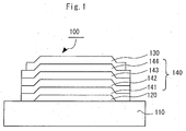
- Fig. 1 is a cross-sectional view showing an example of a conventional organic EL element 100.
- the organic EL element 100 includes a substrate 110, an anode 120 formed on the substrate 110, an organic functional layer 140 made of a plurality of layers laminated on the anode 120, and a cathode 130 formed on the organic functional layer 140.
- the organic functional layer 140 is a functional layer including at least a light-emitting layer.
- the organic functional layer 140 includes a hole injection layer 141, a hole transport layer 142, a light-emitting layer 143, and an electron injection layer 144, layered in this order on top of the anode 120.
- the organic EL element 100 When a voltage is applied between the anode 120 and the cathode 130, holes are injected into the light-emitting layer 143 via the hole transport layer 142 from the anode 120 or the hole injection layer 141, while at the same time electrons are injected into the light-emitting layer 143 from the cathode 130 or the electron injection layer 144. Inside the light-emitting layer 143, the holes and electrons recombine, forming excitons. Within an extremely short time, the excitons fall to a lower energy level, and some emit the energy difference between the lower energy level and the excited state as light. The light given off within this light-emitting layer 143 is emitted to the side of the substrate 110 or to the side of the cathode 130. Thus, the organic EL element 100 functions as a light-emitting element.
- Figs. 2A and 2B illustrate this dielectric breakdown due to defects.
- This organic EL element 200 is fabricated by forming an anode 220 on a substrate 210, then forming an organic functional layer 230 and an organic functional layer 240, followed by forming a cathode 250.
- a pinhole 245, which is a defect has developed in the organic functional layer 240 during the film formation process, and this pinhole 245 is filled by the cathode 250.
- vapor deposition processes have poor step coverage (i.e. ability to cover steps), so that film defects are easily incurred by scratches in the substrate or foreign matter on the substrate.
- One of the issues addressed by the present invention is the problem that shorts occur between anode and cathode due to dielectric breakdown, as described above.
- An organic EL element includes an anode, a cathode, and a light-emitting organic EL layer sandwiched between the anode and the cathode, and includes at least a leak prevention layer that takes on a high resistance when its temperature is increased.
- An organic EL element according to the present invention is provided with a light-emitting organic EL layer, sandwiched between an anode and a cathode.
- This organic EL layer includes at least a leak prevention layer that takes on a high resistance when its temperature is raised.
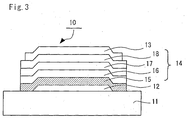
- Fig. 3 is a cross-sectional view showing an organic EL element 10 as an embodiment of the present invention.
- This organic EL element 10 includes a substrate 11, an anode formed on the substrate 11, an organic functional layer 14 made of a plurality of layers layered on the anode 12, and a cathode 13 formed on the organic functional layer 14.
- the organic functional layer 14 includes, in order from the side of the anode 13, a hole injection layer 15, a hole transport layer 16, a light-emitting layer 17, and an electron injection layer 18.
- the hole injection layer 15 injects holes via the hole transport layer 16 into the light-emitting layer 17.
- the electron injection layer 18 injects electrons into the light-emitting layer 17.
- the holes and electron recombine, forming excitons.
- the excitons fall to a lower energy level, and some emit the energy difference between the lower energy level and the excited state as light.
- the light given off within this light-emitting layer 17 is emitted to the side of the substrate 11 or to the side of the cathode 13.
- the organic EL element 10 functions as a light-emitting element.
- the hole injection layer 15 functions as a hole injection layer injecting holes via the hole transport layer 16 into the light-emitting layer 17.
- the hole injection layer 15 functions as a leak prevention layer that suppresses excessive currents.
- the hole injection layer 15 is made of a material whose specific resistance increases at least in a high temperature region that exceeds the maximum working temperature of the product (maximum operating temperature or maximum storage temperature), thus taking on a high resistance. Consequently, the hole injection layer 15 takes on a high resistance as a result of the generation of Joule heat due to current concentration caused by defects. Thus, the current is curbed, and the element can be protected from such damage as dielectric breakdown.
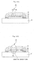
- Figs. 4A and 4B are diagrammatic views illustrating the effect of the leak prevention layer.
- the organic functional layer is shown as being made only of two layers, namely the leak prevention layer and the other layers.
- the organic EL element 20 is fabricated by forming an anode 22 on a substrate 21, then forming a leak prevention layer 23 and an organic functional layer 24, followed by forming a cathode 25.
- the leak prevention layer 23 is made of a material whose specific resistance increases at least in a high temperature region that exceeds the maximum working temperature of the product (maximum operating temperature or maximum storage temperature), thus taking on a high resistance.
- this organic EL element 20 there is a pinhole 24a, which is a defect, formed during the film formation process in the organic functional layer 24, and this pinhole 24a is filled up by the cathode 25.
- the hole injection layer 15 was configured as a leak prevention layer, but the leak prevention layer may be provided at any position of the organic functional layer.
- the leak prevention layer does not only prevent current concentrations, but may also perform a part of the functions of the organic EL element during ordinary operation, such as injection or transport of carriers (electrons or holes). Consequently, in order to increase the element efficiency of the overall organic EL element, it is necessary to appropriately set the ionization potential, the carrier mobility etc. in accordance with the location where it is placed.
- a leak prevention layer that is arranged closer to the cathode than the light-emitting layer needs to have high electron transport abilities
- a leak prevention layer that is arranged closer to the anode than the light-emitting layer needs to have high hole transport abilities
- the layers other than the leak prevention layer are made of a low-molecular weight material, and if the leak prevention layer is made by a wet film formation process, such as spin-coating or printing, or by a film formation process causing considerable damage to the substrate, such as sputtering, then it is preferable that the leak prevention layer is formed first.
- organic materials of low molecular weight have a low resistance to solvents and a low heat resistance. Consequently, when the organic functional layers other than the leak prevention layer, which are made of organic materials of low molecular weight, are formed, and then the leak prevention layer is formed by one of the above-mentioned processes, then there is the possibility that the organic functional layers other than the leak prevention layer are damaged.
- a leak prevention layer with hole transport capability is formed directly on the anode.
- a leak prevention layer with electron transport capability is formed directly on the cathode.
- the leak prevention layer is increased takes on a high resistance at temperatures above 120°C.
- the working temperature range of ordinary organic EL elements is up to about 100°C, so that it becomes possible to inhibit failure of the element due to current concentrations by letting it take on a high resistance at temperatures higher than that.
- the leak prevention layer takes on a high resistance at temperatures above 200°C.
- the working temperature range of organic EL elements is up to about 100°C, the organic EL element may become 120 to 200°C during use, due to Joule heat generated by the current flowing through the organic EL element and heat generation from locations outside the organic EL element, such as driving circuitry.
- the driving of the organic EL element it is better not to let it take on a high resistance up to 200°C.
- the leak prevention layer takes on a high resistance at temperatures less than 400°C, and it is even more preferable that it takes on a high resistance at temperatures less than 300°C.
- the Al used for the cathode has melted, so that it seems that defect portions occur where the temperature has risen locally and temporarily to the melting point of Al (about 660°C).
- the leak prevention layer itself is decomposed, and its weight is reduced fast, so that it loses the capability to prevent shorts.
- the taking on of a high resistance by the leak prevention layer occurs at temperatures at which it is not helpful in order to prevent shorts. Ordinarily, it is effective that it takes on a high resistance in a temperature region of about 300 to 400°C.
- the leak prevention layer takes on a high resistance at temperatures of 120 to 400°C, and it is even more preferable that it takes on a high resistance at temperatures of 200 to 300°C.
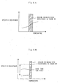
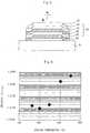
- Figs. 5A and 5B are graphs illustrating the resistance of the leak prevention layer as a function of temperature.
- the resistance of the leak prevention layer exhibits a steep rate of change in the region of temperatures at which it takes on a high resistance.
- the change in the region of temperatures at which it takes on a high resistance region in which high resistance is taken on
- the leak prevention layer acts as a fuse in the defect portions, and it is desirable that the resistance of the leak prevention layer increases sharply in the region of temperatures at which a high resistance is taken on, as in Fig. 5B.
- the leak prevention layer takes on a high resistance means that Joule heat due to current concentrations increases the resistance of the leak prevention layer considerably to an extent at which no shorts occur between the electrodes.
- the resistance of the leak prevention layer alone needs to be increased to a resistance equivalent to that of the entire organic functional layer of a normal portion, in order to lessen the current concentration. In other words, it needs to be increased to a resistance equivalent to the anode-cathode resistance during normal operation. That is, the following expression has to be satisfied: (resistance of leak prevention layer when taking on a high resistance) ⁇ (resistance of organic functional layer at ordinary temperature)
- the resistance of the leak prevention layer should change in the process of shifting from ordinary temperatures to high resistances cannot be said unconditionally, because it depends on the structure of the element, but in general, it is preferable that the resistance is increased by at least one order of magnitude, or becomes insulating (specific resistance of at least 10 11 ⁇ cm) when taking on a high resistance.
- the leak prevention layer prevents breakdown of the organic EL element caused by defect portions formed unintentionally in other layers constituting the organic functional layer. Consequently, there should not be any defects in the leak prevention layer itself. However, when there are uneven portions due to scratches or foreign matter on the substrate, then common defects occur easily in the layers constituting the organic functional layer, so that there is the possibility that defects occur in the leak prevention layer itself. If a large number of defects occur in the leak prevention layer, then it may not be capable of preventing shorts even when taking on a high resistance due to Joule heat.
- the leak prevention layer has a step coverage that is as least as good as that of the other organic functional layers, and that it has few pinholes.
- a wet film formation process such as spin-coating or printing
- a vapor-phase film formation process with good wraparound such as CVD.
- the leak prevention layer is fabricated by a film formation process with high directionality and poor step coverage, such as vapor deposition, then it is preferable to provide the film with good step coverage by after-processing.
- spin-coating refers to methods of dropping a flowable material onto a rotating layering surface, and applying that material uniformly on the layering surface by centrifugal force.
- printing refers to methods such as flexography.
- CVD chemical vapor deposition
- vapor deposition refers to methods in which small pieces of metal or non-metal are evaporated by heating in a high vacuum, and quasi-adhered as a thin film on a primer surface, such as glass, a quartz plate, a cleaved crystal or the like.
- Figs. 6A and 6B show an example of an after-treatment process for improving the step coverage of a leak prevention layer formed by vapor deposition.
- a film formation process with poor step coverage such as vapor deposition
- the leak prevention layer is formed on the upper surface of protrusions and the bottom surface of depressions, but the leak prevention layer is difficult to form at the lateral surfaces of the protrusions and depressions. For this reason, the layer below the leak prevention layer is exposed, and it is difficult to completely cover the layer below it completely with the leak prevention layer.
- the leak prevention layer is heated in an after-treatment to a temperature close to the glass transition point or melting point of the material constituting the leak prevention layer. Due to this heating, the leak prevention layer is melted and shifted, covering the exposed layer below it. Thus, the surface of the leak prevention layer is smoothened, pinholes are eliminated, and it becomes possible to improve its step coverage.
- the leak prevention layer is thick, then there are few pinholes and the step coverage is good, so that it is possible to attain a film with few defects.
- the resistance of the leak prevention layer in the film thickness direction is proportional to the product of specific resistance and film thickness of the leak prevention layer, so that if the leak prevention layer is thick, the effect of taking on a high resistance due to high temperatures at defect portions is even more pronounced, which is preferable.
- the leak prevention layer is thick and its resistance in film thickness direction becomes large, then the driving voltage of the element at ordinary portions is increased. Moreover, if the leak prevention layer is formed such that it is common to and there is full contact between adjacent pixels, then, if the film thickness of the leak prevention layer is too thick, the resistance in horizontal direction (sheet resistance) of the leak prevention layer becomes small, and there is the possibility that adjacent pixels becomes electrically shorted.
- the sheet resistance of the leak prevention layer is proportional to (specific resistance/film thickness).
- the leak prevention layer is thin, then the resistance of the leak prevention layer in film thickness direction becomes small, and the driving voltage of the element at ordinary portions is decreased. However, if the leak prevention layer is thin, there are more pinholes, and the step coverage becomes poor, so that the film will contain many defects. Furthermore, the resistance of the leak prevention layer in the film thickness direction becomes small, so that there is the possibility that the effect of taking on a high resistance due to high temperatures at defect portions becomes small.
- the thickness of the leak prevention layer it is preferable that the resistance in thickness direction of the leak prevention layer after it has taken on a high resistance at high temperatures is set to be larger than the resistance in thickness direction of the organic functional layer in the regular portions (outside the leak prevention layer). Furthermore, it is preferable that the leak prevention layer is so thick that no defects occur in it. As a range fulfilling these conditions, it is preferable that the film thickness of the leak prevention layer is for example about 100 ⁇ .
- the sheet resistance of the leak prevention layer is preferably at least 1 M ⁇ cm, more preferably at least 10 M ⁇ cm, and even more preferably at least 100 M ⁇ cm.
- a polymer material whose conductivity has been increased by doping it with an acid. More specifically, it is possible to use a conductive polymer, such as polyaniline, polypyrrole, polythiophene or polyfuran. These polymers may be doped with an acid in order to elevate their conductivity. When these polymers are heated to a high temperature, the doped acid is de-doped, and their resistance increases, so that their conductivity decreases. These materials ordinarily can be formed into a film by spin-coating or printing.
- acids with which these polymers can be doped it is possible to use inorganic acids, such as hydrochloric acid, sulfuric acid or nitric acid, or acetic acid, formic acid or oxalic acid.
- inorganic acids such as hydrochloric acid, sulfuric acid or nitric acid, or acetic acid, formic acid or oxalic acid.
- an organic semiconductor that takes on a high resistance by thermally decomposing is also possible. More specifically, it is possible to use an organic semiconductor such as a TCNQ (7,7,8,8-tetracyanoquinomethane) complex. When this type of organic semiconductor is heated to a high temperature, it thermally decomposes and takes on a high resistance. With these materials, it is possible to form films by vapor deposition. After the film has been formed by vapor deposition, it is possible to decrease defects such as pinholes and to improve its step coverage by subjecting it to a heating treatment, as described above.
- TCNQ 7,7,8,8-tetracyanoquinomethane
- a cathode 32 is formed on a substrate 31, and layered on top thereof is an organic functional layer 34 including, in that order, an electron injection layer 35, a light-emitting layer 36, a hole transport layer 37 and a hole injection layer 38.
- An anode 33 is formed on the hole injection layer 38.
- the electron injection layer 35 functions as an electron injection layer for injecting electrons into the light-emitting layer 36 in an ordinary working temperature region, and functions as a leak prevention layer suppressing excessive currents.
- the electron injection layer 35 is made of a material whose specific resistance increases at least in a high temperature region that exceeds the maximum working temperature of the product (maximum operating temperature or maximum storage temperature), thus taking on a high resistance. Consequently, the electron injection layer 35 takes on a high resistance by the generation of Joule heat due to current concentration caused by defects. Thus, the current is curbed, and the element can be protected from such damage as dielectric breakdown.
- Fig. 8 shows another modified embodiment of the present invention.
- a cathode 42 is formed on a substrate 41, and layered on top thereof is an organic functional layer 44 including, in that order, an electron injection layer 45, a light-emitting layer 46, a hole transport layer 47 and a hole injection layer 48.
- An anode 43 is formed on the hole injection layer 48.
- the electron injection layer 45 functions as an electron injection layer for injecting electrons into the light-emitting layer 46 in an ordinary working temperature region, and also functions as a leak prevention layer suppressing excessive currents.
- the hole injection layer 48 functions as a hole injection layer for injecting holes into the light-emitting layer 46 in an ordinary working temperature region, and also functions as a leak prevention layer suppressing excessive currents.
- the electron injection layer 45 and the hole injection layer 48 are made of materials whose specific resistance increases at least in a high temperature region that exceeds the maximum working temperature of the product (maximum operating temperature or maximum storage temperature), thus taking on a high resistance.
- the electron injection layer 45 and the hole injection layer 48 take on a high resistance by the generation of Joule heat due to current concentration caused by defects. Therefore, the current is curbed, and the element can be protected from such damage as dielectric breakdown. It is thus also possible to provide the organic functional layer with two or more leak prevention layers.
- Example 1 an organic EL element was fabricated with the following procedure.
- An ITO film of 1500 ⁇ thickness was formed by sputtering on a glass substrate. Then, the photoresist AZ6112 (by Tokyo Ohka Kogyo, Co., Ltd.) was patterned on the ITO film. The resulting substrate was immersed in a mixture of a ferric chloride aqueous solution and hydrochloric acid, and the portion of the ITO not covered by the resist was etched away. After that, the glass substrate was immersed in acetone to remove the resist, thus obtaining a predetermined ITO electrode pattern.
- a coating liquid of a polyaniline derivative doped with acid dissolved in an organic solvent was spin-coated onto the glass substrate of (1).
- the coating liquid adhering to terminal portions outside the display portion of the substrate was removed by wiping it off, and then the substrate was heated with a hot plate to evaporate the solvent, thus obtaining a polyaniline film (leak prevention layer) of 450 ⁇ thickness.
- a NPABP film of 250 ⁇ and an Alq3 film of 600 ⁇ thickness were formed by vapor deposition on the glass substrate of (2) as the organic functional films besides the leak prevention layer. Furthermore, an Al-Li alloy film of 1000 ⁇ thickness was formed by vapor deposition as the cathode, thus concluding the organic EL element.
- the size of the organic EL element defined by the intersection of anode and cathode was 2 mm ⁇ 2 mm.
- an organic EL element was prepared in the same manner as in Example 1, except that Step (2) of Example 1 was not performed (that is, no leak prevention layer was formed), and the film thickness of the NPABP in Step (3) was set to 700 ⁇ .
- the organic EL element of Example 1 and the organic EL element of Comparative Example 1 had the same total film thickness.
- a polyaniline film was formed on glass substrates in the same manner as in Step (2) of Embodiment 1, thus preparing samples. These samples were heated for 5 min with a hot plate to various temperatures. The sheet resistance of the heated samples was measured by the two-terminal method, and their film thickness was measured with a Dektak stylus profilometer, and their respective specific resistance was determined from the measurement results.
- Fig. 9 is a graph showing the relation between the heating temperature and the specific resistance of the polyaniline film.
- the specific resistance of the polyaniline derivative film increases roughly by a factor of 100. It seems that this is a result of the doped acid being de-doped due to heat, leading to a sharp increase in resistance.
- the resistance of this polyaniline film increases sharply to take on a high resistance, showing that the polyaniline film is suitable as a leak prevention layer.
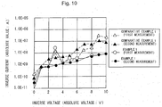
- a reverse voltage (anode to minus and cathode to plus) was applied to the elements fabricated in Example 1 and Comparative Example 1, and the current flowing through the elements was measured. The measurement was carried out twice per sample. The measurement results are shown in Fig. 10.
- Example 1 In the element of Example 1, a rise in current can be observed that appears to be caused by shorts between anode and cathode near 3 V and 5 V at the first measurement, but the current immediately returns to normal values. It seems that a large current temporarily flowed at defect portions, but the effect of the leak prevention layer lessened the current concentration. At the second measurement, no rise in current could be observed, and smooth characteristics with small current values are attained. It seems that this is because the defect portions that appeared when a voltage was applied for the first time were repaired by the leak prevention layer.
- An organic EL display panel was manufactured with the following procedure.
- An ITO film of 1500 ⁇ thickness was formed by sputtering on a glass substrate. Then, the photoresist AZ6112 (by Tokyo Ohka Kogyo, Co., Ltd.) was patterned on the ITO film. The resulting substrate was immersed in a mixture of a ferric chloride aqueous solution and hydrochloric acid, and the portion of the ITO not covered by the resist was etched away. After that, the glass substrate was immersed in acetone, to remove the resist, thus obtaining a stripe-shaped electrode pattern made of 256 lines.
- a coating liquid of a polyaniline derivative doped with acid dissolved in an organic solvent was spin-coated in the glass substrate of (1).
- the coating liquid adhering to terminal portions outside the display portion of the substrate was removed by wiping it off, and then the substrate was heated with a hot plate to evaporate the solvent, thus obtaining a polyaniline film (leak prevention layer) of 450 ⁇ thickness.
- a NPABP film of 250 ⁇ and an Alq3 film of 600 ⁇ thickness were formed by vapor deposition on the glass substrate of (2) as the organic functional films besides the leak prevention layer. Furthermore, an Al-Li alloy film of 1000 ⁇ thickness was formed by vapor deposition as the cathode, using a mask made of a striped pattern with 64 stripes. The size of one dot defined by the intersection of anodes and cathodes was 0.3 mm ⁇ 0.3 mm, and there were 256 ⁇ 64 dots.
- a sealing plate having a desiccant fixed to its depression portions was laminated with an adhesive against the substrate of Step (3), thus forming a passively driven organic EL display panel.
- Example 2 an organic EL panel with 256 ⁇ 64 dots was prepared in the same manner as in Example 2, except that Step (2) of Example 2 was not performed (that is, no leak prevention layer was formed), and the film thickness of the NPABP was set to 700 ⁇ .
- the organic EL elements of Example 2 and the organic EL elements of Comparative Example 1 had the same total film thickness.
- Example 2 The panels fabricated in Example 2 and Comparative Example 2 were connected to a predetermined driving circuit, and after operating them continuously for 500 hours under a 85°C atmosphere, the number of dots that have become defective as a result of shorts between anode and cathode were counted.
- the results were as follows:
- an organic EL element includes an anode, a cathode, and a light-emitting organic EL layer sandwiched between the anode and the cathode, the organic EL layer having at least a leak prevention layer that takes on a high resistance when its temperature is increased. Consequently, even when there is an excessive current caused by defects in the organic functional layer, the leak prevention layer takes on a high resistance as a result of the heat generated by the excessive current, and the current is curbed, so that element breakdown caused by defects of the organic EL element can be prevented before it occurs.
- step coverage of the leak prevention layer is made at least equivalent to that of the other layers, so that the leak prevention layer can cover defect portions in the organic functional layer, and the effect of the present invention can be improved even further.
Landscapes
- Physics & Mathematics (AREA)
- Optics & Photonics (AREA)
- Electroluminescent Light Sources (AREA)
Abstract
In order to prevent shorts between anode and cathode
by dielectric breakdown in an organic EL element, the
organic EL layer includes a leak prevention layer that
takes on a high resistance when its temperature is
increased.
Description
The present invention relates to organic
electroluminescent elements.
Organic EL (electroluminescent) elements having a
structure in which an organic functional layer is
sandwiched between an anode and a cathode are known as one
type of light-emitting thin film elements.
Fig. 1 is a cross-sectional view showing an example
of a conventional organic EL element 100. The organic EL
element 100 includes a substrate 110, an anode 120 formed
on the substrate 110, an organic functional layer 140 made
of a plurality of layers laminated on the anode 120, and a
cathode 130 formed on the organic functional layer 140.
The organic functional layer 140 is a functional
layer including at least a light-emitting layer. In Fig.
1, the organic functional layer 140 includes a hole
injection layer 141, a hole transport layer 142, a light-emitting
layer 143, and an electron injection layer 144,
layered in this order on top of the anode 120.
When a voltage is applied between the anode 120 and
the cathode 130, holes are injected into the light-emitting
layer 143 via the hole transport layer 142 from the anode
120 or the hole injection layer 141, while at the same time
electrons are injected into the light-emitting layer 143
from the cathode 130 or the electron injection layer 144.
Inside the light-emitting layer 143, the holes and
electrons recombine, forming excitons. Within an extremely
short time, the excitons fall to a lower energy level, and
some emit the energy difference between the lower energy
level and the excited state as light. The light given off
within this light-emitting layer 143 is emitted to the side
of the substrate 110 or to the side of the cathode 130.
Thus, the organic EL element 100 functions as a light-emitting
element.
However, when there are defect locations in this
conventional organic EL element, such as pinholes or
partially thinner film thickness, then the resistance at
those defect locations becomes lower than at other
portions, and current (electrons or holes) concentrates at
those defect locations. This results in the problem that
the buildup of Joule heat and the increase in the strength
of the electric field due to such concentrations causes
dielectric breakdown at the defect locations, and
ultimately leads to shorts between the anode and the
cathode.
Figs. 2A and 2B illustrate this dielectric breakdown
due to defects. This organic EL element 200 is fabricated
by forming an anode 220 on a substrate 210, then forming an
organic functional layer 230 and an organic functional
layer 240, followed by forming a cathode 250. In the
organic EL element 200 in Fig. 2A, a pinhole 245, which is
a defect, has developed in the organic functional layer 240
during the film formation process, and this pinhole 245 is
filled by the cathode 250.
When a voltage is applied to this organic EL element
200 having such a defect, current concentrates at a portion
235 within the organic functional layer 230 located
directly below the pinhole 245 resulting in a large
electric field. When this state continues, dielectric
breakdown occurs in the portion 235 within the organic
functional layer 220, as shown in Fig. 2B, the anode 220
and the cathode 250 are shorted, and the organic EL element
200 cannot function as a light-emitting element anymore.
When an organic EL element having such a defect is used for
a display panel or the like, the display quality of the
display panel is severely damaged, and its value as a
product is diminished.
The above-described defect tends to occur in
particular when organic functional layers are formed by a
vapor deposition process. Ordinarily, vapor deposition
processes have poor step coverage (i.e. ability to cover
steps), so that film defects are easily incurred by
scratches in the substrate or foreign matter on the
substrate.
One of the issues addressed by the present invention
is the problem that shorts occur between anode and cathode
due to dielectric breakdown, as described above.
An organic EL element according to one aspect of the
present invention includes an anode, a cathode, and a
light-emitting organic EL layer sandwiched between the
anode and the cathode, and includes at least a leak
prevention layer that takes on a high resistance when its
temperature is increased.
The following is a detailed description of
embodiments of an organic EL element according to the
present invention.
An organic EL element according to the present
invention is provided with a light-emitting organic EL
layer, sandwiched between an anode and a cathode. This
organic EL layer includes at least a leak prevention layer
that takes on a high resistance when its temperature is
raised. The following is a more detailed explanation of an
organic EL element according to this embodiment, with
reference to the accompanying drawings.
Fig. 3 is a cross-sectional view showing an organic
EL element 10 as an embodiment of the present invention.
This organic EL element 10 includes a substrate 11, an
anode formed on the substrate 11, an organic functional
layer 14 made of a plurality of layers layered on the anode
12, and a cathode 13 formed on the organic functional layer
14.
The organic functional layer 14 includes, in order
from the side of the anode 13, a hole injection layer 15, a
hole transport layer 16, a light-emitting layer 17, and an
electron injection layer 18. When a voltage is applied,
the hole injection layer 15 injects holes via the hole
transport layer 16 into the light-emitting layer 17. And
when a voltage is applied, the electron injection layer 18
injects electrons into the light-emitting layer 17. Within
the light-emitting layer 17, the holes and electron
recombine, forming excitons. Within an extremely short
time, the excitons fall to a lower energy level, and some
emit the energy difference between the lower energy level
and the excited state as light. The light given off within
this light-emitting layer 17 is emitted to the side of the
substrate 11 or to the side of the cathode 13. Thus, the
organic EL element 10 functions as a light-emitting
element.
Within an ordinary working temperature region, the
hole injection layer 15 functions as a hole injection layer
injecting holes via the hole transport layer 16 into the
light-emitting layer 17. On the other hand, in a
temperature region that is higher than the ordinary working
temperature region, it functions as a leak prevention layer
that suppresses excessive currents. The hole injection
layer 15 is made of a material whose specific resistance
increases at least in a high temperature region that
exceeds the maximum working temperature of the product
(maximum operating temperature or maximum storage
temperature), thus taking on a high resistance.
Consequently, the hole injection layer 15 takes on a high
resistance as a result of the generation of Joule heat due
to current concentration caused by defects. Thus, the
current is curbed, and the element can be protected from
such damage as dielectric breakdown.
Figs. 4A and 4B are diagrammatic views illustrating
the effect of the leak prevention layer. Here, to simplify
the explanations, the organic functional layer is shown as
being made only of two layers, namely the leak prevention
layer and the other layers.
In Fig. 4A, the organic EL element 20 is fabricated
by forming an anode 22 on a substrate 21, then forming a
leak prevention layer 23 and an organic functional layer
24, followed by forming a cathode 25. Here, the leak
prevention layer 23 is made of a material whose specific
resistance increases at least in a high temperature region
that exceeds the maximum working temperature of the product
(maximum operating temperature or maximum storage
temperature), thus taking on a high resistance.
Furthermore, in this organic EL element 20, there is a
pinhole 24a, which is a defect, formed during the film
formation process in the organic functional layer 24, and
this pinhole 24a is filled up by the cathode 25.
When voltage is applied to the organic EL element 20
having such a defect, current concentrates at a portion 23a
within the leak prevention layer 23 that is located
directly below the pinhole 24a, resulting in a large
electric field. This current concentration causes a large
Joule heat, which increases the temperature of the leak
prevention layer beyond the maximum working temperature.
As shown in Fig. 4B, this temperature increase causes the
specific resistance of the leak prevention layer 23 to
rise, so that the leak prevention layer 23 takes on a high
resistance. Consequently, the current flowing in the leak
prevention layer 23 is decreased, lessening the heat
generation and the electric field in the leak prevention
layer (thermal repair). Thus, by providing a layer
functioning as a leak prevention layer as one layer of the
organic functional layer, current concentrations at one
location within the organic functional layer can be
prevented, and breakdown of the organic EL element 20 can
be prevented.
In Fig. 3, the hole injection layer 15 was configured
as a leak prevention layer, but the leak prevention layer
may be provided at any position of the organic functional
layer. As mentioned before, the leak prevention layer does
not only prevent current concentrations, but may also
perform a part of the functions of the organic EL element
during ordinary operation, such as injection or transport
of carriers (electrons or holes). Consequently, in order
to increase the element efficiency of the overall organic
EL element, it is necessary to appropriately set the
ionization potential, the carrier mobility etc. in
accordance with the location where it is placed. For
example, a leak prevention layer that is arranged closer to
the cathode than the light-emitting layer needs to have
high electron transport abilities, and a leak prevention
layer that is arranged closer to the anode than the light-emitting
layer needs to have high hole transport abilities.
The layers other than the leak prevention layer are
made of a low-molecular weight material, and if the leak
prevention layer is made by a wet film formation process,
such as spin-coating or printing, or by a film formation
process causing considerable damage to the substrate, such
as sputtering, then it is preferable that the leak
prevention layer is formed first. Ordinarily, organic
materials of low molecular weight have a low resistance to
solvents and a low heat resistance. Consequently, when the
organic functional layers other than the leak prevention
layer, which are made of organic materials of low molecular
weight, are formed, and then the leak prevention layer is
formed by one of the above-mentioned processes, then there
is the possibility that the organic functional layers other
than the leak prevention layer are damaged.
More concretely, in the case of an organic EL element
in which the anode is arranged on the substrate, it is
preferable that a leak prevention layer with hole transport
capability is formed directly on the anode. And in the
case of an organic EL element in which the cathode is
arranged on the substrate, it is preferable that a leak
prevention layer with electron transport capability is
formed directly on the cathode.
It is preferable that the leak prevention layer is
increased takes on a high resistance at temperatures above
120°C. The working temperature range of ordinary organic
EL elements is up to about 100°C, so that it becomes
possible to inhibit failure of the element due to current
concentrations by letting it take on a high resistance at
temperatures higher than that.
Furthermore, it is even more preferable that the leak
prevention layer takes on a high resistance at temperatures
above 200°C. Even though the working temperature range of
organic EL elements is up to about 100°C, the organic EL
element may become 120 to 200°C during use, due to Joule
heat generated by the current flowing through the organic
EL element and heat generation from locations outside the
organic EL element, such as driving circuitry. Thus, in
order to not hinder the driving of the organic EL element
during ordinary operation, it is better not to let it take
on a high resistance up to 200°C.
It is preferable that the leak prevention layer takes
on a high resistance at temperatures less than 400°C, and
it is even more preferable that it takes on a high
resistance at temperatures less than 300°C. When examining
portions where a short has developed between anode and
cathode in conventional organic EL elements, it can be seen
how the Al used for the cathode has melted, so that it
seems that defect portions occur where the temperature has
risen locally and temporarily to the melting point of Al
(about 660°C). Ordinarily, in high temperature regions,
such as above 500°C, the leak prevention layer itself is
decomposed, and its weight is reduced fast, so that it
loses the capability to prevent shorts. Consequently, it
is not preferable that the taking on of a high resistance
by the leak prevention layer occurs at temperatures at
which it is not helpful in order to prevent shorts.
Ordinarily, it is effective that it takes on a high
resistance in a temperature region of about 300 to 400°C.
In conclusion, it is preferable that the leak
prevention layer takes on a high resistance at temperatures
of 120 to 400°C, and it is even more preferable that it
takes on a high resistance at temperatures of 200 to 300°C.
Figs. 5A and 5B are graphs illustrating the
resistance of the leak prevention layer as a function of
temperature. Here, it is preferable that the resistance of
the leak prevention layer exhibits a steep rate of change
in the region of temperatures at which it takes on a high
resistance. When the change in the region of temperatures
at which it takes on a high resistance (region in which
high resistance is taken on) is smooth as in Fig. 5A, then
the lessening of the current at the defect portions
proceeds slowly, so that the influence of the Joule heat
extends to the areas around the defect portions. Ideally,
the leak prevention layer acts as a fuse in the defect
portions, and it is desirable that the resistance of the
leak prevention layer increases sharply in the region of
temperatures at which a high resistance is taken on, as in
Fig. 5B.
Here, that the leak prevention layer takes on a high
resistance means that Joule heat due to current
concentrations increases the resistance of the leak
prevention layer considerably to an extent at which no
shorts occur between the electrodes. When a defect portion
has assumed a high temperature due to current
concentration, the resistance of the leak prevention layer
alone needs to be increased to a resistance equivalent to
that of the entire organic functional layer of a normal
portion, in order to lessen the current concentration. In
other words, it needs to be increased to a resistance
equivalent to the anode-cathode resistance during normal
operation. That is, the following expression has to be
satisfied:
(resistance of leak prevention layer when taking on a
high resistance) ≥ (resistance of organic functional layer
at ordinary temperature)
To what extent the resistance of the leak prevention
layer should change in the process of shifting from
ordinary temperatures to high resistances cannot be said
unconditionally, because it depends on the structure of the
element, but in general, it is preferable that the
resistance is increased by at least one order of magnitude,
or becomes insulating (specific resistance of at least
1011Ω·cm) when taking on a high resistance.
The leak prevention layer prevents breakdown of the
organic EL element caused by defect portions formed
unintentionally in other layers constituting the organic
functional layer. Consequently, there should not be any
defects in the leak prevention layer itself. However, when
there are uneven portions due to scratches or foreign
matter on the substrate, then common defects occur easily
in the layers constituting the organic functional layer, so
that there is the possibility that defects occur in the
leak prevention layer itself. If a large number of defects
occur in the leak prevention layer, then it may not be
capable of preventing shorts even when taking on a high
resistance due to Joule heat.
Considering the above, it is preferable that the leak
prevention layer has a step coverage that is as least as
good as that of the other organic functional layers, and
that it has few pinholes. In order to form a film with
good step coverage and few pinholes, it is preferable to
form the leak prevention layer by a wet film formation
process, such as spin-coating or printing, or by a vapor-phase
film formation process with good wraparound, such as
CVD.
Furthermore, if the leak prevention layer is
fabricated by a film formation process with high
directionality and poor step coverage, such as vapor
deposition, then it is preferable to provide the film with
good step coverage by after-processing.
Here, "spin-coating" refers to methods of dropping a
flowable material onto a rotating layering surface, and
applying that material uniformly on the layering surface by
centrifugal force. Furthermore, "printing" refers to
methods such as flexography.
Furthermore, "CVD (chemical vapor deposition)" refers
to methods in which a vapor of the molecules of a reaction
system or a mixed vapor of such molecules and an inactive
carrier is flowed onto a heated substrate, and the reaction
product from a reaction such as hydrolysis, autolysis,
photolysis, oxidation-reduction, or substitution is
deposited on the substrate.
Furthermore, "vapor deposition" refers to methods in
which small pieces of metal or non-metal are evaporated by
heating in a high vacuum, and quasi-adhered as a thin film
on a primer surface, such as glass, a quartz plate, a
cleaved crystal or the like.
Figs. 6A and 6B show an example of an after-treatment
process for improving the step coverage of a leak
prevention layer formed by vapor deposition. As shown in
Fig. 6A, when a film formation process with poor step
coverage, such as vapor deposition, is used, then the leak
prevention layer is formed on the upper surface of
protrusions and the bottom surface of depressions, but the
leak prevention layer is difficult to form at the lateral
surfaces of the protrusions and depressions. For this
reason, the layer below the leak prevention layer is
exposed, and it is difficult to completely cover the layer
below it completely with the leak prevention layer.
In order to correct this deficiency, the leak
prevention layer is heated in an after-treatment to a
temperature close to the glass transition point or melting
point of the material constituting the leak prevention
layer. Due to this heating, the leak prevention layer is
melted and shifted, covering the exposed layer below it.
Thus, the surface of the leak prevention layer is
smoothened, pinholes are eliminated, and it becomes
possible to improve its step coverage.
Here, if the leak prevention layer is thick, then
there are few pinholes and the step coverage is good, so
that it is possible to attain a film with few defects.
Also, the resistance of the leak prevention layer in the
film thickness direction is proportional to the product of
specific resistance and film thickness of the leak
prevention layer, so that if the leak prevention layer is
thick, the effect of taking on a high resistance due to
high temperatures at defect portions is even more
pronounced, which is preferable.
However, if the leak prevention layer is thick and
its resistance in film thickness direction becomes large,
then the driving voltage of the element at ordinary
portions is increased. Moreover, if the leak prevention
layer is formed such that it is common to and there is full
contact between adjacent pixels, then, if the film
thickness of the leak prevention layer is too thick, the
resistance in horizontal direction (sheet resistance) of
the leak prevention layer becomes small, and there is the
possibility that adjacent pixels becomes electrically
shorted. The sheet resistance of the leak prevention layer
is proportional to (specific resistance/film thickness).
If the leak prevention layer is thin, then the
resistance of the leak prevention layer in film thickness
direction becomes small, and the driving voltage of the
element at ordinary portions is decreased. However, if the
leak prevention layer is thin, there are more pinholes, and
the step coverage becomes poor, so that the film will
contain many defects. Furthermore, the resistance of the
leak prevention layer in the film thickness direction
becomes small, so that there is the possibility that the
effect of taking on a high resistance due to high
temperatures at defect portions becomes small.
Considering the above, as a lower limit for the
thickness of the leak prevention layer it is preferable
that the resistance in thickness direction of the leak
prevention layer after it has taken on a high resistance at
high temperatures is set to be larger than the resistance
in thickness direction of the organic functional layer in
the regular portions (outside the leak prevention layer).
Furthermore, it is preferable that the leak prevention
layer is so thick that no defects occur in it. As a range
fulfilling these conditions, it is preferable that the film
thickness of the leak prevention layer is for example about
100Å.
Furthermore, if the leak prevention layer is formed
such that it is common to and there is full contact between
adjacent pixels, then it is preferable that adjacent pixels
are not shorted and no cross-talk occurs. The range
fulfilling this condition depends on the size of the gap
between adjacent pixels, but to be specific, the sheet
resistance of the leak prevention layer is preferably at
least 1 MΩ·cm, more preferably at least 10 MΩ·cm, and even
more preferably at least 100 MΩ·cm.
As a material for the leak prevention layer
fulfilling these conditions, it is possible to use a
polymer material whose conductivity has been increased by
doping it with an acid. More specifically, it is possible
to use a conductive polymer, such as polyaniline,
polypyrrole, polythiophene or polyfuran. These polymers
may be doped with an acid in order to elevate their
conductivity. When these polymers are heated to a high
temperature, the doped acid is de-doped, and their
resistance increases, so that their conductivity decreases.
These materials ordinarily can be formed into a film by
spin-coating or printing.
As acids with which these polymers can be doped, it
is possible to use inorganic acids, such as hydrochloric
acid, sulfuric acid or nitric acid, or acetic acid, formic
acid or oxalic acid.
It is also possible to use an organic semiconductor
that takes on a high resistance by thermally decomposing as
the material for the leak prevention layer. More
specifically, it is possible to use an organic
semiconductor such as a TCNQ (7,7,8,8-tetracyanoquinomethane)
complex. When this type of organic
semiconductor is heated to a high temperature, it thermally
decomposes and takes on a high resistance. With these
materials, it is possible to form films by vapor
deposition. After the film has been formed by vapor
deposition, it is possible to decrease defects such as
pinholes and to improve its step coverage by subjecting it
to a heating treatment, as described above.
A modified embodiment of the present invention will
now be described.
In the above-described embodiment, a structure was
shown in which the anode is formed on the substrate, but
the present invention is not limited thereto, and it can
also be applied to structures in which the cathode is
formed on the substrate. An example of this is depicted as
a modified embodiment in Fig. 7.
In the organic EL element in Fig. 7, a cathode 32 is
formed on a substrate 31, and layered on top thereof is an
organic functional layer 34 including, in that order, an
electron injection layer 35, a light-emitting layer 36, a
hole transport layer 37 and a hole injection layer 38. An
anode 33 is formed on the hole injection layer 38.
In the organic EL element in Fig. 7, the electron
injection layer 35 functions as an electron injection layer
for injecting electrons into the light-emitting layer 36 in
an ordinary working temperature region, and functions as a
leak prevention layer suppressing excessive currents. The
electron injection layer 35 is made of a material whose
specific resistance increases at least in a high
temperature region that exceeds the maximum working
temperature of the product (maximum operating temperature
or maximum storage temperature), thus taking on a high
resistance. Consequently, the electron injection layer 35
takes on a high resistance by the generation of Joule heat
due to current concentration caused by defects. Thus, the
current is curbed, and the element can be protected from
such damage as dielectric breakdown.
Fig. 8 shows another modified embodiment of the
present invention. In the organic EL element in Fig. 8, a
cathode 42 is formed on a substrate 41, and layered on top
thereof is an organic functional layer 44 including, in
that order, an electron injection layer 45, a light-emitting
layer 46, a hole transport layer 47 and a hole
injection layer 48. An anode 43 is formed on the hole
injection layer 48.
In the organic EL element in Fig. 8, the electron
injection layer 45 functions as an electron injection layer
for injecting electrons into the light-emitting layer 46 in
an ordinary working temperature region, and also functions
as a leak prevention layer suppressing excessive currents.
Furthermore, the hole injection layer 48 functions as a
hole injection layer for injecting holes into the light-emitting
layer 46 in an ordinary working temperature
region, and also functions as a leak prevention layer
suppressing excessive currents. The electron injection
layer 45 and the hole injection layer 48 are made of
materials whose specific resistance increases at least in a
high temperature region that exceeds the maximum working
temperature of the product (maximum operating temperature
or maximum storage temperature), thus taking on a high
resistance. Consequently, the electron injection layer 45
and the hole injection layer 48 take on a high resistance
by the generation of Joule heat due to current
concentration caused by defects. Therefore, the current is
curbed, and the element can be protected from such damage
as dielectric breakdown. It is thus also possible to
provide the organic functional layer with two or more leak
prevention layers.
The following is an explanation of a manufacturing
method of the embodiments of the organic EL element
according to the present invention. However, it should be
noted that the present invention is not limited to the
examples described below.
In Example 1, an organic EL element was fabricated
with the following procedure.
An ITO film of 1500Å thickness was formed by
sputtering on a glass substrate. Then, the photoresist
AZ6112 (by Tokyo Ohka Kogyo, Co., Ltd.) was patterned on
the ITO film. The resulting substrate was immersed in a
mixture of a ferric chloride aqueous solution and
hydrochloric acid, and the portion of the ITO not covered
by the resist was etched away. After that, the glass
substrate was immersed in acetone to remove the resist,
thus obtaining a predetermined ITO electrode pattern.
A coating liquid of a polyaniline derivative doped
with acid dissolved in an organic solvent was spin-coated
onto the glass substrate of (1). The coating liquid
adhering to terminal portions outside the display portion
of the substrate was removed by wiping it off, and then the
substrate was heated with a hot plate to evaporate the
solvent, thus obtaining a polyaniline film (leak prevention
layer) of 450Å thickness.
A NPABP film of 250Å and an Alq3 film of 600Å
thickness were formed by vapor deposition on the glass
substrate of (2) as the organic functional films besides
the leak prevention layer. Furthermore, an Al-Li alloy
film of 1000Å thickness was formed by vapor deposition as
the cathode, thus concluding the organic EL element. The
size of the organic EL element defined by the intersection
of anode and cathode was 2 mm × 2 mm.
As Comparative Example 1, an organic EL element was
prepared in the same manner as in Example 1, except that
Step (2) of Example 1 was not performed (that is, no leak
prevention layer was formed), and the film thickness of the
NPABP in Step (3) was set to 700Å. The organic EL element
of Example 1 and the organic EL element of Comparative
Example 1 had the same total film thickness.
A polyaniline film was formed on glass substrates in
the same manner as in Step (2) of Embodiment 1, thus
preparing samples. These samples were heated for 5 min
with a hot plate to various temperatures. The sheet
resistance of the heated samples was measured by the two-terminal
method, and their film thickness was measured with
a Dektak stylus profilometer, and their respective specific
resistance was determined from the measurement results.
Fig. 9 is a graph showing the relation between the
heating temperature and the specific resistance of the
polyaniline film. At 250 to 300°C, the specific resistance
of the polyaniline derivative film increases roughly by a
factor of 100. It seems that this is a result of the doped
acid being de-doped due to heat, leading to a sharp
increase in resistance. Thus, at a temperature region of
250 to 300°C, the resistance of this polyaniline film
increases sharply to take on a high resistance, showing
that the polyaniline film is suitable as a leak prevention
layer.
A reverse voltage (anode to minus and cathode to
plus) was applied to the elements fabricated in Example 1
and Comparative Example 1, and the current flowing through
the elements was measured. The measurement was carried out
twice per sample. The measurement results are shown in
Fig. 10.
In the element of Example 1, a rise in current can be
observed that appears to be caused by shorts between anode
and cathode near 3 V and 5 V at the first measurement, but
the current immediately returns to normal values. It seems
that a large current temporarily flowed at defect portions,
but the effect of the leak prevention layer lessened the
current concentration. At the second measurement, no rise
in current could be observed, and smooth characteristics
with small current values are attained. It seems that this
is because the defect portions that appeared when a voltage
was applied for the first time were repaired by the leak
prevention layer.
On the other hand, in the element of Comparative
Example 1, there is a rise in current at both the first and
the second measurement that appears to stem from shorts
between anode and cathode, and there is no sign that the
defects are repaired. Thus, it was found that the
breakdown of the element due to current concentrations is
prevented by providing a leak prevention layer.
An organic EL display panel was manufactured with the
following procedure.
An ITO film of 1500Å thickness was formed by
sputtering on a glass substrate. Then, the photoresist
AZ6112 (by Tokyo Ohka Kogyo, Co., Ltd.) was patterned on
the ITO film. The resulting substrate was immersed in a
mixture of a ferric chloride aqueous solution and
hydrochloric acid, and the portion of the ITO not covered
by the resist was etched away. After that, the glass
substrate was immersed in acetone, to remove the resist,
thus obtaining a stripe-shaped electrode pattern made of
256 lines.
A coating liquid of a polyaniline derivative doped
with acid dissolved in an organic solvent was spin-coated
in the glass substrate of (1). The coating liquid adhering
to terminal portions outside the display portion of the
substrate was removed by wiping it off, and then the
substrate was heated with a hot plate to evaporate the
solvent, thus obtaining a polyaniline film (leak prevention
layer) of 450Å thickness.
A NPABP film of 250Å and an Alq3 film of 600Å
thickness were formed by vapor deposition on the glass
substrate of (2) as the organic functional films besides
the leak prevention layer. Furthermore, an Al-Li alloy
film of 1000Å thickness was formed by vapor deposition as
the cathode, using a mask made of a striped pattern with 64
stripes. The size of one dot defined by the intersection
of anodes and cathodes was 0.3 mm × 0.3 mm, and there were
256 × 64 dots.
Under a dry nitrogen atmosphere, a sealing plate
having a desiccant fixed to its depression portions was
laminated with an adhesive against the substrate of Step
(3), thus forming a passively driven organic EL display
panel.
As Comparative Example 2, an organic EL panel with
256 × 64 dots was prepared in the same manner as in Example
2, except that Step (2) of Example 2 was not performed
(that is, no leak prevention layer was formed), and the
film thickness of the NPABP was set to 700Å. The organic
EL elements of Example 2 and the organic EL elements of
Comparative Example 1 had the same total film thickness.
The panels fabricated in Example 2 and Comparative
Example 2 were connected to a predetermined driving
circuit, and after operating them continuously for 500
hours under a 85°C atmosphere, the number of dots that have
become defective as a result of shorts between anode and
cathode were counted. The results were as follows:
- Panel of Example 2: Number of Defect Dots: 0
- Panel of Comparative Example 2: Number of Defect Dots: 16
Consequently, it was confirmed that in the panel of Example
2, which has a leak prevention layer, there were fewer
defects due to shorts than in the panel of Comparative
Example 2, which does not have a leak prevention layer.
As described above, an organic EL element according
to an embodiment of the present invention includes an
anode, a cathode, and a light-emitting organic EL layer
sandwiched between the anode and the cathode, the organic
EL layer having at least a leak prevention layer that takes
on a high resistance when its temperature is increased.
Consequently, even when there is an excessive current
caused by defects in the organic functional layer, the leak
prevention layer takes on a high resistance as a result of
the heat generated by the excessive current, and the
current is curbed, so that element breakdown caused by
defects of the organic EL element can be prevented before
it occurs.
Furthermore, the step coverage of the leak prevention
layer is made at least equivalent to that of the other
layers, so that the leak prevention layer can cover defect
portions in the organic functional layer, and the effect of
the present invention can be improved even further.
Claims (12)
- An organic EL element comprising an anode, a cathode, and a light-emitting organic EL layer sandwiched between said anode and said cathode;
wherein said organic EL layer comprises a leak prevention layer that takes on a high resistance when its temperature is increased. - The organic EL element according to claim 1, wherein said leak prevention layer has hole transport abilities, and transports holes from the anode side to the cathode side.
- The organic EL element according to claim 1 or 2, wherein said leak prevention layer has electron transport abilities, and transports electrons from said cathode side to said anode side.
- The organic EL element according to claim 1 or 2, wherein said leak prevention layer is arranged in contact with said anode.
- The organic EL element according to claim 1 or 3, wherein said leak prevention layer is arranged in contact with said cathode.
- The organic EL element according to any of claims 1 to 5, wherein said leak prevention layer takes on a high resistance at temperatures of at least 120°C.
- The organic EL element according to claim 6, wherein said leak prevention layer takes on a high resistance at temperatures of 120 to 400°C.
- The organic EL element according to claim 7, wherein said leak prevention layer takes on a high resistance at temperatures of 200 to 300°C.
- The organic EL element according to any of claims 1 to 8, wherein, when taking on a high resistance, the specific resistance of said leak prevention layer increases at least by a factor of 10.
- The organic EL element according to any of claims 1 to 8, wherein, when taking on a high resistance, the specific resistance of said leak prevention layer becomes at least 1011Ω·cm.
- The organic EL element according to any of claims 1 to 10, wherein said leak prevention layer is made of a conductive polymer that is doped with an acid.
- The organic EL element according to any of claims 1 to 11, wherein said leak prevention layer is made by a wet film formation process or a vapor-phase film formation process.
Applications Claiming Priority (3)
| Application Number | Priority Date | Filing Date | Title |
|---|---|---|---|
| JP2002255661A JP2004095388A (en) | 2002-08-30 | 2002-08-30 | Organic EL device |
| JP2002255661 | 2002-08-30 | ||
| PCT/JP2003/010299 WO2004021746A1 (en) | 2002-08-30 | 2003-08-13 | Organic el element |
Publications (2)
| Publication Number | Publication Date |
|---|---|
| EP1549110A1 true EP1549110A1 (en) | 2005-06-29 |
| EP1549110A4 EP1549110A4 (en) | 2009-06-24 |
Family
ID=31972906
Family Applications (1)
| Application Number | Title | Priority Date | Filing Date |
|---|---|---|---|
| EP03791212A Withdrawn EP1549110A4 (en) | 2002-08-30 | 2003-08-13 | Organic el element |
Country Status (8)
| Country | Link |
|---|---|
| US (1) | US20060033427A1 (en) |
| EP (1) | EP1549110A4 (en) |
| JP (1) | JP2004095388A (en) |
| KR (1) | KR100714428B1 (en) |
| CN (2) | CN1695403A (en) |
| AU (1) | AU2003255027A1 (en) |
| TW (1) | TWI226206B (en) |
| WO (1) | WO2004021746A1 (en) |
Cited By (5)
| Publication number | Priority date | Publication date | Assignee | Title |
|---|---|---|---|---|
| WO2006036297A3 (en) * | 2004-09-17 | 2006-09-14 | 3M Innovative Properties Co | Organic electroluminescence device and method of production of same |
| WO2009127174A1 (en) | 2008-04-15 | 2009-10-22 | Novaled Ag | Light emitting organic component with fuse structure |
| WO2009127175A1 (en) * | 2008-04-15 | 2009-10-22 | Novaled Ag | Light-emitting organic component, arrangement having a plurality of light-emitting organic components and electrode structure |
| WO2009133501A1 (en) * | 2008-04-29 | 2009-11-05 | Philips Intellectual Property & Standards Gmbh | Oled device with current limiting layer |
| WO2011044867A3 (en) * | 2009-10-14 | 2011-07-14 | Novaled Ag | Electro-optical, organic semiconductor component and method for the production thereof |
Families Citing this family (14)
| Publication number | Priority date | Publication date | Assignee | Title |
|---|---|---|---|---|
| US7183707B2 (en) * | 2004-04-12 | 2007-02-27 | Eastman Kodak Company | OLED device with short reduction |
| JP2007012504A (en) * | 2005-07-01 | 2007-01-18 | Toppan Printing Co Ltd | Organic EL device manufacturing method and organic EL device |
| JP2007066707A (en) * | 2005-08-31 | 2007-03-15 | Denso Corp | Manufacturing method of organic EL element |
| JP2009021073A (en) * | 2007-07-11 | 2009-01-29 | Sumitomo Chemical Co Ltd | Self-luminous element, lighting device and display device |
| JP2009021104A (en) * | 2007-07-12 | 2009-01-29 | Sumitomo Chemical Co Ltd | Manufacturing method of organic light emitting device |
| JP5007170B2 (en) * | 2007-07-20 | 2012-08-22 | 株式会社ジャパンディスプレイイースト | Organic EL display device |
| CN101964354B (en) * | 2010-08-20 | 2012-05-23 | 友达光电股份有限公司 | Organic light-emitting device, lighting device, and liquid crystal display |
| US20130168665A1 (en) * | 2010-10-20 | 2013-07-04 | Ocean's King Lighting Science & Techning | Organic electroluminescent device and manufacturing method thereof |
| CN102082165B (en) * | 2010-11-05 | 2013-04-17 | 友达光电股份有限公司 | Organic light-emitting device and manufacturing method thereof |
| TWI552411B (en) * | 2013-04-01 | 2016-10-01 | 樂金顯示科技股份有限公司 | Organic light emitting device and method of manufacturing same |
| KR101946999B1 (en) * | 2014-05-12 | 2019-02-12 | 엘지디스플레이 주식회사 | Organic light emitting device and method for manufacturing the same |
| KR101925574B1 (en) * | 2014-05-15 | 2018-12-05 | 엘지디스플레이 주식회사 | Organic light emitting device |
| JP2017062884A (en) | 2015-09-24 | 2017-03-30 | ソニー株式会社 | Display device and light emitting device |
| JP2022124486A (en) * | 2021-02-15 | 2022-08-25 | 日本放送協会 | Electronic element, electrochromic element, electroluminescent element, display and lighting device |
Family Cites Families (11)
| Publication number | Priority date | Publication date | Assignee | Title |
|---|---|---|---|---|
| DE1490659B2 (en) * | 1964-09-17 | 1972-01-13 | Siemens AG, 1000 Berlin u. 8000 München | SINTERED ELECTRIC COLD CONDUCTOR RESISTOR BODY AND PROCESS FOR ITS MANUFACTURING |
| US3932313A (en) * | 1973-12-28 | 1976-01-13 | Texas Instruments Incorporated | Process for manufacture of positive temperature coefficient materials |
| JPH04297076A (en) * | 1991-01-31 | 1992-10-21 | Toshiba Corp | Organic el element |
| US6713955B1 (en) * | 1998-11-20 | 2004-03-30 | Agilent Technologies, Inc. | Organic light emitting device having a current self-limiting structure |
| JP2000348868A (en) * | 1999-04-01 | 2000-12-15 | Dainippon Printing Co Ltd | EL element and method of recording / erasing / displaying light emitting display pattern thereof |
| US6366017B1 (en) * | 1999-07-14 | 2002-04-02 | Agilent Technologies, Inc/ | Organic light emitting diodes with distributed bragg reflector |
| JP2001160492A (en) * | 1999-12-06 | 2001-06-12 | Japan Science & Technology Corp | Organic thin-film electroluminescence device and driving method thereof |
| SG96550A1 (en) * | 2000-04-24 | 2003-06-16 | Inst Materials Research & Eng | Blue electroluminescent materials for polymer light-emitting diodes |
| JP2001319788A (en) * | 2000-05-11 | 2001-11-16 | Matsushita Electric Ind Co Ltd | EL device |
| JP4696355B2 (en) * | 2000-12-08 | 2011-06-08 | Tdk株式会社 | Organic EL device |
| JP2002324683A (en) * | 2001-04-25 | 2002-11-08 | Rohm Co Ltd | Organic EL element and organic EL display using the same |
-
2002
- 2002-08-30 JP JP2002255661A patent/JP2004095388A/en active Pending
-
2003
- 2003-08-13 CN CNA038247577A patent/CN1695403A/en active Pending
- 2003-08-13 AU AU2003255027A patent/AU2003255027A1/en not_active Abandoned
- 2003-08-13 EP EP03791212A patent/EP1549110A4/en not_active Withdrawn
- 2003-08-13 WO PCT/JP2003/010299 patent/WO2004021746A1/en not_active Ceased
- 2003-08-13 US US10/525,822 patent/US20060033427A1/en not_active Abandoned
- 2003-08-13 KR KR1020057003467A patent/KR100714428B1/en not_active Expired - Fee Related
- 2003-08-18 TW TW092122607A patent/TWI226206B/en not_active IP Right Cessation
- 2003-09-01 CN CNU032080050U patent/CN2653833Y/en not_active Expired - Fee Related
Cited By (8)
| Publication number | Priority date | Publication date | Assignee | Title |
|---|---|---|---|---|
| WO2006036297A3 (en) * | 2004-09-17 | 2006-09-14 | 3M Innovative Properties Co | Organic electroluminescence device and method of production of same |
| WO2009127174A1 (en) | 2008-04-15 | 2009-10-22 | Novaled Ag | Light emitting organic component with fuse structure |
| WO2009127175A1 (en) * | 2008-04-15 | 2009-10-22 | Novaled Ag | Light-emitting organic component, arrangement having a plurality of light-emitting organic components and electrode structure |
| US8203263B2 (en) | 2008-04-15 | 2012-06-19 | Novaled Ag | Light emitting organic component with fuse structure |
| US8466457B2 (en) | 2008-04-15 | 2013-06-18 | Novaled Ag | Light-emitting organic component, arrangement having a plurality of light-emitting organic components and electrode structure |
| EP2816628A3 (en) * | 2008-04-15 | 2015-03-04 | Novaled GmbH | Light-emitting organic component and arrangement having a plurality of light-emitting organic components |
| WO2009133501A1 (en) * | 2008-04-29 | 2009-11-05 | Philips Intellectual Property & Standards Gmbh | Oled device with current limiting layer |
| WO2011044867A3 (en) * | 2009-10-14 | 2011-07-14 | Novaled Ag | Electro-optical, organic semiconductor component and method for the production thereof |
Also Published As
| Publication number | Publication date |
|---|---|
| JP2004095388A (en) | 2004-03-25 |
| US20060033427A1 (en) | 2006-02-16 |
| TWI226206B (en) | 2005-01-01 |
| EP1549110A4 (en) | 2009-06-24 |
| CN1695403A (en) | 2005-11-09 |
| WO2004021746A1 (en) | 2004-03-11 |
| AU2003255027A1 (en) | 2004-03-19 |
| KR20050057041A (en) | 2005-06-16 |
| KR100714428B1 (en) | 2007-05-07 |
| TW200404480A (en) | 2004-03-16 |
| CN2653833Y (en) | 2004-11-03 |
Similar Documents
| Publication | Publication Date | Title |
|---|---|---|
| EP1549110A1 (en) | Organic el element | |
| US8310152B2 (en) | Organic EL device and EL display panel having a low driving voltage and high light emitting frequency, and method for manufacturing | |
| KR100597698B1 (en) | Display elements | |
| EP2077698B1 (en) | Organic el device and method for manufacturing the same | |
| US7160633B2 (en) | Structure-defining materials for OLEDs | |
| US6416885B1 (en) | Electroluminescent device | |
| US6879099B2 (en) | Organic EL element and organic EL display | |
| JP2002532848A (en) | Organic light emitting devices | |
| US8247963B2 (en) | Organic electroluminescent display device and production method thereof | |
| KR100853897B1 (en) | Organic electroluminescent element | |
| US20040253368A1 (en) | Manufacturing method of display device | |
| US20050282308A1 (en) | Organic electroluminescent display device and method of producing the same | |
| JP3893774B2 (en) | Electroluminescent device and manufacturing method thereof | |
| KR100581645B1 (en) | Polymer-Type Organic Electroluminescence Display Device | |
| US20090127546A1 (en) | Organic light emitting diode and method for the production thereof | |
| KR20060086884A (en) | Organic EL element, method for manufacturing same and organic EL display device | |
| JP2003045665A (en) | Organic el display device | |
| JP2005071634A (en) | Display panel | |
| KR20060084210A (en) | Organic EL element | |
| HK1051439A (en) | Electroluminescent device |
Legal Events
| Date | Code | Title | Description |
|---|---|---|---|
| PUAI | Public reference made under article 153(3) epc to a published international application that has entered the european phase |
Free format text: ORIGINAL CODE: 0009012 |
|
| 17P | Request for examination filed |
Effective date: 20050318 |
|
| AK | Designated contracting states |
Kind code of ref document: A1 Designated state(s): AT BE BG CH CY CZ DE DK EE ES FI FR GB GR HU IE IT LI LU MC NL PT RO SE SI SK TR |
|
| AX | Request for extension of the european patent |
Extension state: AL LT LV MK |
|
| DAX | Request for extension of the european patent (deleted) | ||
| RBV | Designated contracting states (corrected) |
Designated state(s): DE FR GB |
|
| A4 | Supplementary search report drawn up and despatched |
Effective date: 20090528 |
|
| STAA | Information on the status of an ep patent application or granted ep patent |
Free format text: STATUS: THE APPLICATION HAS BEEN WITHDRAWN |
|
| 18W | Application withdrawn |
Effective date: 20090805 |