EP1549037A1 - An active impedance synthesis circuit, for example for XDSL splitters - Google Patents
An active impedance synthesis circuit, for example for XDSL splitters Download PDFInfo
- Publication number
- EP1549037A1 EP1549037A1 EP03029556A EP03029556A EP1549037A1 EP 1549037 A1 EP1549037 A1 EP 1549037A1 EP 03029556 A EP03029556 A EP 03029556A EP 03029556 A EP03029556 A EP 03029556A EP 1549037 A1 EP1549037 A1 EP 1549037A1
- Authority
- EP
- European Patent Office
- Prior art keywords
- arrangement
- impedance
- transfer function
- function element
- secondary winding
- Prior art date
- Legal status (The legal status is an assumption and is not a legal conclusion. Google has not performed a legal analysis and makes no representation as to the accuracy of the status listed.)
- Granted
Links
- 230000015572 biosynthetic process Effects 0.000 title claims abstract description 27
- 238000003786 synthesis reaction Methods 0.000 title claims abstract description 27
- 238000004804 winding Methods 0.000 claims abstract description 45
- 238000012546 transfer Methods 0.000 claims abstract description 28
- 238000001228 spectrum Methods 0.000 claims abstract description 5
- 230000001747 exhibiting effect Effects 0.000 claims abstract description 3
- 238000001914 filtration Methods 0.000 claims description 9
- 238000002347 injection Methods 0.000 claims description 8
- 239000007924 injection Substances 0.000 claims description 8
- 230000009471 action Effects 0.000 claims description 5
- 238000013459 approach Methods 0.000 description 10
- 239000000243 solution Substances 0.000 description 8
- 239000003990 capacitor Substances 0.000 description 6
- 238000007667 floating Methods 0.000 description 6
- 238000010586 diagram Methods 0.000 description 5
- 238000005516 engineering process Methods 0.000 description 5
- 230000008901 benefit Effects 0.000 description 4
- 230000008878 coupling Effects 0.000 description 3
- 238000010168 coupling process Methods 0.000 description 3
- 238000005859 coupling reaction Methods 0.000 description 3
- 230000000694 effects Effects 0.000 description 3
- 230000009467 reduction Effects 0.000 description 3
- 239000008186 active pharmaceutical agent Substances 0.000 description 2
- 230000005540 biological transmission Effects 0.000 description 2
- 238000004891 communication Methods 0.000 description 2
- 230000007423 decrease Effects 0.000 description 2
- 238000013461 design Methods 0.000 description 2
- 238000007688 edging Methods 0.000 description 2
- 230000010354 integration Effects 0.000 description 2
- 238000012360 testing method Methods 0.000 description 2
- 238000012937 correction Methods 0.000 description 1
- 238000003780 insertion Methods 0.000 description 1
- 230000037431 insertion Effects 0.000 description 1
- 238000009434 installation Methods 0.000 description 1
- 238000005259 measurement Methods 0.000 description 1
- 230000003071 parasitic effect Effects 0.000 description 1
- 238000012545 processing Methods 0.000 description 1
- 230000003595 spectral effect Effects 0.000 description 1
- 230000002194 synthesizing effect Effects 0.000 description 1
- 238000011144 upstream manufacturing Methods 0.000 description 1
Images



Classifications
-
- H—ELECTRICITY
- H03—ELECTRONIC CIRCUITRY
- H03H—IMPEDANCE NETWORKS, e.g. RESONANT CIRCUITS; RESONATORS
- H03H11/00—Networks using active elements
- H03H11/02—Multiple-port networks
- H03H11/40—Impedance converters
-
- H—ELECTRICITY
- H04—ELECTRIC COMMUNICATION TECHNIQUE
- H04L—TRANSMISSION OF DIGITAL INFORMATION, e.g. TELEGRAPHIC COMMUNICATION
- H04L27/00—Modulated-carrier systems
- H04L27/26—Systems using multi-frequency codes
- H04L27/2601—Multicarrier modulation systems
Definitions
- the invention relates primarily to xDSL (i.e. X Digital Subscriber Line) splitter applications. However, the invention is adapted for use, in general, in filtering applications or in synthesizing floating impedances through an ELF (Extremely Low Frequency) decoupled circuitry.
- xDSL i.e. X Digital Subscriber Line
- ELF Extremely Low Frequency
- Figure 1 of the drawing shows the general layout of a "splitter" for xDSL systems that separates xDSL and POTS/ISDN systems by means of a bi-directional filtering action.
- the acronyms shown in the figure and the functions performed by the functional blocks designated thereby are well known to those of skill in the art, thus making it unnecessary to provide a detailed description herein
- XDSL technology can co-exist with other communication channels like POTS and ISDN, which share the same cable/loop placed between CO and CPE as shown in figure 1
- the typical bandwidth used in xDSL applications ranges from 20 ⁇ 130KHz to 1 ⁇ 11MHz whereas POTS/ISDN applications involve frequencies from DC to 20 ⁇ 130KHz.
- Different signals are allocated in the low frequency band too (DC ⁇ 50Hz), such as:
- the basic aim of a splitter is to separate xDSL signals from POTS/ISDN signals. Specifically, the splitter attenuates spurious signals falling in the xDSL band due to POTS/ISDN events like on/off-hook, ringer, ring injection, ring trip dial pulses and so on, while vice versa avoids that xDSL signals may reach the POTS/ISDN port showing high impedance in the xDSL band.
- a splitter is usually comprised by a HPF and a LPF: the former is used as xDSL-loop interface by cutting out frequencies lower than 30KHz - 130KHz, the latter acts as a POTS/ISDN-loop interface avoiding noise injection in xDSL band (from POTS to loop) and providing, in the same bandwidth, an high impedance seen from loop to POTS.
- ADSL CO modems already include a CO HPF.
- splitter will apply primarily to the LPF part only.
- US-A-5 627 501 adopts a passive approach implemented with a low pass filter (LPF) plus a variable impedance circuit.
- LPF low pass filter
- a measurement unit placed on the ADSL side detects the LPF coil saturation and inserts additional impedance that limits the POTS current flow. This solution is not applicable for stand-alone splitter requiring the ADSL system supervision; additionally, expensive additional components such as switches must be added.
- US-B-6 144 735 provides a solution based on a configurable filter. It makes extensive use of passive components plus an off-hook detector network that switches the splitter in two different filtering states.
- US-B-6 628 783 provides an active solution without supply and able to suppress (with a depletion MOS device) high frequency spurious signals due to POTS events. It requires a HV MOS with low R ON value and a 3 rd order extra passive section to satisfy standard splitter requirements.
- US-A-5 889 856 discloses a purely digital approach applicable only to COMBO arrangements that offer a single termination point on the CO-side.
- An analog splitter is not required but the complexity of the digital part is increased.
- analog circuitry (which is not easy to integrate) is required provide DC feed, battery voltage and ring.
- the object of the present invention is thus to provide an improved solution dispensing with the intrinsic disadvantages of the prior art arrangements considered in the foregoing.
- a preferred basic embodiment of the invention is thus an arrangement including:
- said current source is controlled by the transfer function element via a feedback path and the associated gain element is a distributed gain over said feedback path.
- the current source is connected to a current injection point selected out of:
- Preferred embodiments provide for the transfer function element being connected to sense voltage at said secondary winding.
- the transfer function element is connected to a terminal of the secondary winding. This is preferably via said gain element and/or a voltage divider.
- the transfer function element is connected for on-line sensing voltage across an impedance in series with said primary winding.
- a general aim of this invention is implementing impedance on HV wires by reducing the number of HV components/devices.
- Figure 2 shows the basic idea underlying the invention.
- a transformer T provides the DC decoupling between the HV and LV circuit sections.
- Blocks K, H, g build the synthesis around the secondary winding L 2 that is mirrored on the primary winding L 1 arranged on the HV wire.
- FIG. 3 shows a block schematic of an xDSL splitter, based on the synthesis circuit shown above, with a reduced set of passive devices.
- the whole splitter is implemented with only two passive devices, the transformer T and a capacitor C, plus a LV-part (elements K, H, g, to be detailed in the following) that is completely integrable without specific technological requirements.
- block H programmable permits the realisation of desired impedance values without changing the external components, thus supporting splitter functionalities for multi xDSL platform.
- an advantage offered by the arrangement described herein lies in the reduction of the splitter board space due to the low number of passive devices used.
- component integration dashed box
- the whole circuit seen at terminals A, B can be ideally thought as a floating AC-impedance realized with the active blocks H, K, g.
- the stage K is intended as a distributed gain on the whole feedback path
- g is a VCCS (Voltage Controlled Current Source)
- H(s) a module (essentially comprised of one or more filters) whose transfer functions determines the "shape" (i.e. the frequency spectrum) of the impedance Zsh over the frequency field.
- the synthesis circuit works around L 2 and sends/receives signals to/from the branch A, B through the magnetic coupling with L 1 .
- the equation system in Eq 1 helps in understanding the concept and can be used to calculate the synthesized impedance seen from one of the two terminals when grounding the other one:
- the signal v 2 (on the LV side) contains information about current flowing in the primary winding L 1 (placed on the HV branch).
- the signal v 2 is processed by the active part and is then transferred via mutual coupling (M) to the HV side, without a direct DC coupling with the line.
- Eq 2 and Eq 3 highlight that the impedance Zsh is modelled around sL 1 acting on ⁇ and shaped in terms of frequency range through the transfer function H(s).
- H(s) the transfer function
- the value for Alpha permits to increase, decrease or invert the sL 1 impedance, depending on application. synthesis effect on sL1 vs. conditions on alpha.
- Stability can be analysed by taking the single ended case of figure 5 as a reference. Generally, both terminals A and B of the floating synthesized impedance are loaded towards ground via impedances Z A and Z B that play an important role in stability. In the situation considered the open loop gain (G OL ) may extracted by cutting the path feedback at the point indicated with a cross [X] and by solving the circuit with respect the ratio v ox /v ix .
- the single ended circuit can be substituted by an equivalent circuit.
- This equivalent circuit is comprised of the synthesized impedance with a noise generator e no 2 connected in series.
- e ni 2 denotes the equivalent input noise at the input of the block K
- POTS & ISDN splitters represent a natural field of application for the described impedance synthesizer. In fact, both LV and HV signals flow in splitters but the filtering actions must be activated only on the LV component. In other words, splitters should be transparent for HV signals and provide high impedance for LV signals as specified in the standards already mentioned in the introductory portion of the description.
- a splitter based on a hybrid arrangement as shown in figure 3 represents an optimum trade off in terms of performance, consumption, cost and complexity.
- the active splitter described herein is based on a simple architecture comprised of a transformer T, acting as a ELF (Extremely Low Frequency) decoupler and an active part able to synthesize an impedance around L 2 in a frequency range higher than the ELF range considered.
- ELF Extremely Low Frequency
- the transformer T will 'block' the DC as well as the ring signal from L 1 to L 2 .
- the supply requirements of the active-part will be determined only from the choice of the winding ratio' n and the PSD masks of the ADSL and Voice signals normally present on line.
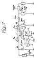
- Figure 7 gives a simplified single-ended block schematic of a xDSL's system adapted to create a model.
- Synthesis factor this is the ratio of the synthesized impedance and the physically used impedance sL 1 .
- the first choice is neglected while the third one is taken as a guideline.
- Eq 9.3 and Eq 8 indicate H 2 will be a high pass filter (HPF). Moreover, its choice should be done in order to implement a G.992.1 compliant filtering action.
- the band limitation of K and g acts by switching off the synthesis outside the ADSL band reducing power consumption outside the frequency region of interest.
- Zsh determines the active splitter performance in terms of return loss, insertion loss, attenuation distortion, delay distortion, ADSL band attenuation and input impedance (see e.g. ITU-T Recommendation G.992.1 (1999): “Asymmetric Digital Subscriber Line (ADSL)").
- Sensing factor this is a useful parameter to provide the dynamic ranges of signal processed by the active chain vs. the current flowing on primary winding.
- Ksh 1 n ⁇ ( sL 1 ) ⁇
- Ksh Zsh n
- Ks will increase providing a greater signal on the active part.
- a decrement of i 1 which leads to a limited signal v 2 , follows an increment of Ks in the ADSL band.
- Line noise factor this is expressed as the ratio of the on-line injected noise to the equivalent input noise of the active chain including the elements K, H, g.
- ZA and ZB denote the impedances loading the nodes A and B, respectively.
- the above-mentioned factor has the expression in Eq 15. This indicates that a certain care is required in properly selecting the transformer ratio n, as this may multiply the noise injected into node B, which may disturb the ADSL channel.
- H(s) was considered as notionally comprised of three stages: a high pass filter (HPF), a low pass filter (LPF) and a phase adjustment filter (PAD), while the following quantitative parameters have been used.
- HPF high pass filter
- LPF low pass filter
- PAD phase adjustment filter
- H ( s ) H 2HPF ( s ) ⁇ H 2 LPF ( s ) ⁇ H 2 PAD ( s ) ⁇ H 1 ( s )
- H 2 HPF ( s ) s 2 ⁇ 9.0376 ⁇ 10 -1 + 1.6328 ⁇ 10 8 s 2 + s ⁇ 2.1385 ⁇ 10 4 +7.4831 ⁇ 10 9
- H 2HPF is a second order elliptic high pass function with a cut-off frequency of 10kHz and 44dB attenuation, instead H 1 is the function which compensate sL 2 in equation Eq 3
- the PAD filter is unitary, given that no phase correction is needed for this kind of H 2HPF .
- Ksh depends linearly on Alpha, while the previous solutions (Eq 25) convey a hyperbolic relationship.
- Eq 29 shows the open loop gain when terminals P and L are respectively loaded with Z P and Z L ; this formula put in evidence that stability is not an issue when one/both terminals are floating.
- the arrangement described herein achieves a reduction in the passive components needed in filtering applications like xDSL splitter.
- LV technology to integrate active devices, provides a high density solution in terms of area and cost: for instance, a high order filter can be implemented by means of an ASIC, a single transformer plus some SMD components, in the place of a huge transformers chain, thus achieving a substantial saving in PCB space.
Landscapes
- Cable Transmission Systems, Equalization Of Radio And Reduction Of Echo (AREA)
- Filters And Equalizers (AREA)
- Telephonic Communication Services (AREA)
Abstract
Description
- The invention relates primarily to xDSL (i.e. X Digital Subscriber Line) splitter applications. However, the invention is adapted for use, in general, in filtering applications or in synthesizing floating impedances through an ELF (Extremely Low Frequency) decoupled circuitry.
- The instant description will extensively rely on acronyms/abbreviations that are common in the technical area considered. The following is a list of those acronyms/abbreviations provided by way of direct reference, along with short explanations of the corresponding meanings:
- xDSL
- X - Digital Subscriber Line
- POTS
- Plain Old Telephone Service
- PTSN
- Public Switching Telecommunication Network
- ISDN
- Integrated Service Digital Network
- CO
- Central Office
- CPE
- Customer Premise Equipment
- DS
- Down Stream
- UP
- Upstream
- HV
- High Voltage
- LV
- Low Voltage
- LPF
- Low Pass Filter
- HPF
- High Pass Filter
- COMBO
- Integrated POTS and ADSL line cards
- PSD
- Power Spectral Density
- VCCS
- Voltage Controlled Current Source
- ELF
- Extremely Low Frequencies
- PAD
- Phase Adjuster filter
- SMD
- Surface Mounted Device
- GIC
- Generalized Immittance Converter
- Figure 1 of the drawing shows the general layout of a "splitter" for xDSL systems that separates xDSL and POTS/ISDN systems by means of a bi-directional filtering action. The acronyms shown in the figure and the functions performed by the functional blocks designated thereby are well known to those of skill in the art, thus making it unnecessary to provide a detailed description herein
- XDSL technology can co-exist with other communication channels like POTS and ISDN, which share the same cable/loop placed between CO and CPE as shown in figure 1
- The typical bandwidth used in xDSL applications ranges from 20÷130KHz to 1÷11MHz whereas POTS/ISDN applications involve frequencies from DC to 20÷130KHz. Different signals are allocated in the low frequency band too (DC ÷ 50Hz), such as:
- line test signals,
- ringer,
- dial pulsing,
- on/off hook signals, and
- in specific cases, billing tones (12 - 16KHz).
- The basic requirements for a splitter are well known in the art, as witnessed e.g. by the above-referenced ITU-T Recommendation and by additional documents such as:
- ETSI TR 101 728 (V1.1.1): "Access and Terminals (AT); Study for the specification of the low pass section of POTS/ADSL splitters".
- ANSI T1.413: "Network to Customer Installation Interfaces - Asymmetric Digital Subscriber Line (ADSL) Metallic Interface".
- ETSI TS 101 388 (V1.2.1): "Transmission and Multiplexing (TM); Access transmission systems on metallic access cables".
- ETSI TS 101 952 (V1.1.1) : "Part 1: ADSL splitters
for European deployment;
Sub-part 3: Specification of ADSL/ISDN splitters". - ETSI TS 101 952 (V1.1.1): Part 1: ADSL splitters for European deployment; Sub-part 4: Specification of ADSL over "ISDN or POTS universal splitters.
- ITU-T Brugge, Belgium, 17 - 21 June 2002: "Draft Rec. G.992.3 - ADSL2".
- ITU-T Recommendation G.992.5 ASYMMETRIC DIGITAL SUBSCRIBER LINE (ADSL) TRANSCEIVERS - EXTENDED BANDWIDTH ADSL2 (ADSL2plus).
- COMMITTEE T1 - TELECOMMUNICATIONS Working Group T1E1.4 (DSL Access): Very-high-bit-rate Digital Subscriber Line (VDSL) Metallic Interface Part 1: Functional Requirements and Common Specification.
- ETSI TS 101 952-2-3 v1.1.1: "Part 2: VDSL splitters for European deployment; Sub-part 3: Specification of VDSL/ISDN splitters for use at the Local Exchange (LE) and the user side near the Network Termination Port (NTP)".
- ETSI TS 101 952-2-1 v1.1.1: "Part 2: VDSL splitters for European deployment; Sub-part 1: Specification of the low pass part of VDSL/POTS splitters".
-
- The basic aim of a splitter is to separate xDSL signals from POTS/ISDN signals. Specifically, the splitter attenuates spurious signals falling in the xDSL band due to POTS/ISDN events like on/off-hook, ringer, ring injection, ring trip dial pulses and so on, while vice versa avoids that xDSL signals may reach the POTS/ISDN port showing high impedance in the xDSL band.
- A splitter is usually comprised by a HPF and a LPF: the former is used as xDSL-loop interface by cutting out frequencies lower than 30KHz - 130KHz, the latter acts as a POTS/ISDN-loop interface avoiding noise injection in xDSL band (from POTS to loop) and providing, in the same bandwidth, an high impedance seen from loop to POTS.
- Usually, ADSL CO modems already include a CO HPF. In the rest of the instant description, the term splitter will apply primarily to the LPF part only.
- Reference works such as, e.g. J.Cook and P.Sheppard: "ADSL and VDSL Splitter Design and Telephony Performance", IEEE Journal on selected areas in communications, Vol. 13, No.9, December 1995, XDSL show that splitters can be are divided in passive and active categories.
- In the passive case, the a huge presence of HV passive devices is necessary to produce a filter of adequate order (4th÷7th) - see, e.g. US-B-6 144 735 or US-A-5 627 501.
- In the active case - see, e.g. US-A-5 623 543 or US-B-6 628 783 - active devices permit to reduce the order of the passive filter.
- Other arrangements - see, e.g. US-5 627 501 (already cited in the foregoing) or US-A-5 889 856 require digital signal processing.
- The inventors have observed that both the article of Cook and Sheppard and US-A-5 623 543 provide an active approach that implements high performance splitters based on GIC and a line voltage sensing with two HV capacitors. These arrangements do not take into account complexity, density and power consumption (80mW quiescent power).
- US-A-5 627 501 adopts a passive approach implemented with a low pass filter (LPF) plus a variable impedance circuit. A measurement unit placed on the ADSL side detects the LPF coil saturation and inserts additional impedance that limits the POTS current flow. This solution is not applicable for stand-alone splitter requiring the ADSL system supervision; additionally, expensive additional components such as switches must be added.
- US-B-6 144 735 provides a solution based on a configurable filter. It makes extensive use of passive components plus an off-hook detector network that switches the splitter in two different filtering states.
- US-B-6 628 783 provides an active solution without supply and able to suppress (with a depletion MOS device) high frequency spurious signals due to POTS events. It requires a HV MOS with low RON value and a 3rd order extra passive section to satisfy standard splitter requirements.
- US-A-5 889 856 discloses a purely digital approach applicable only to COMBO arrangements that offer a single termination point on the CO-side. An analog splitter is not required but the complexity of the digital part is increased. Additionally, analog circuitry (which is not easy to integrate) is required provide DC feed, battery voltage and ring.
- The object of the present invention is thus to provide an improved solution dispensing with the intrinsic disadvantages of the prior art arrangements considered in the foregoing.
- The present invention achieves that object by means of an arrangement having the features set forth in the claims that follow.
- A preferred basic embodiment of the invention is thus an arrangement including:
- a transformer having a primary winding and a secondary winding, the transformer exhibiting an impedance across said primary winding, and
- an impedance synthesis circuit including:
- a transfer function element having a frequency spectrum, said transfer function element having associated a gain element, and
- a current source controlled by said transfer function element,
- Preferably, said current source is controlled by the transfer function element via a feedback path and the associated gain element is a distributed gain over said feedback path.
- Still preferably, the current source is connected to a current injection point selected out of:
- either terminal of said secondary winding, and
- a point connected to said secondary winding via an impedance.
- Preferred embodiments provide for the transfer function element being connected to sense voltage at said secondary winding. To that effect, the transfer function element is connected to a terminal of the secondary winding. This is preferably via said gain element and/or a voltage divider. Alternatively, the transfer function element is connected for on-line sensing voltage across an impedance in series with said primary winding.
- The invention will now be described, by way of example only, with reference to the annexed figures of drawing, wherein:
- figure 1 has been described previously,
- figure 2 is a block diagram of a synthesis circuit adapted for use in the arrangement described herein,
- figure 3 is a block diagram of an active splitter circuit adapted for use in the arrangement described herein,
- figure 4 is a block diagram of a floating impedance synthesis circuit adapted for use in the arrangement described herein,
- figures 5 and 6 are exemplary block diagrams for stability analysis and noise analysis of the arrangement described herein,
- figure 7 is a simplified system model of the arrangement described herein,
- figure 8 is a block diagram exemplary of the general topology of the arrangement described herein, and
- figure 9 is exemplary of a line current sensing approach for possible application to the arrangement described herein.
- A general aim of this invention is implementing impedance on HV wires by reducing the number of HV components/devices.
- Figure 2 shows the basic idea underlying the invention. There, a transformer T provides the DC decoupling between the HV and LV circuit sections. Blocks K, H, g build the synthesis around the secondary winding L2 that is mirrored on the primary winding L1 arranged on the HV wire.
- Figure 3 shows a block schematic of an xDSL splitter, based on the synthesis circuit shown above, with a reduced set of passive devices. Here, the whole splitter is implemented with only two passive devices, the transformer T and a capacitor C, plus a LV-part (elements K, H, g, to be detailed in the following) that is completely integrable without specific technological requirements.
- This approach leads to an appreciable impact in terms of area reduction of the POTS/ISDN splitter: this is today the main bottleneck in the CO DSLAM line density.
- Moreover, making the block H programmable permits the realisation of desired impedance values without changing the external components, thus supporting splitter functionalities for multi xDSL platform.
- With respect to the prior art, an advantage offered by the arrangement described herein lies in the reduction of the splitter board space due to the low number of passive devices used. In fact, as explained above, component integration (dashed box) on the "active" side, leads to a very compact active POTS/ISDN splitter for xDSL applications.
- Others important advantages relate to:
- the dynamic programmability of the impedance, which permits digital switching from one xDSL technology to another;
- longitudinal balance, only depending on the transformer characteristics;
- flexibility in terms of capability to work in stand-alone mode or in COMBO systems; and
- low cost.
- An explanation of the basic principles underlying the synthesis circuit described herein will represent an introduction to a more detailed description of the exemplary embodiment of the present invention. To that end, the basic equations useful for understanding active splitter structure and operation will be given, while describing application of the circuit to an active splitter.
- The architecture shown in figure 4, exemplifies the concept of impedance synthesizer where a single ended approach for simplicity.
- The whole circuit seen at terminals A, B can be ideally thought as a floating AC-impedance realized with the active blocks H, K, g. The stage K is intended as a distributed gain on the whole feedback path, g is a VCCS (Voltage Controlled Current Source) and H(s) a module (essentially comprised of one or more filters) whose transfer functions determines the "shape" (i.e. the frequency spectrum) of the impedance Zsh over the frequency field.
- The synthesis circuit works around L2 and sends/receives signals to/from the branch A, B through the magnetic coupling with L1. The equation system in Eq 1 helps in understanding the concept and can be used to calculate the synthesized impedance seen from one of the two terminals when grounding the other one:
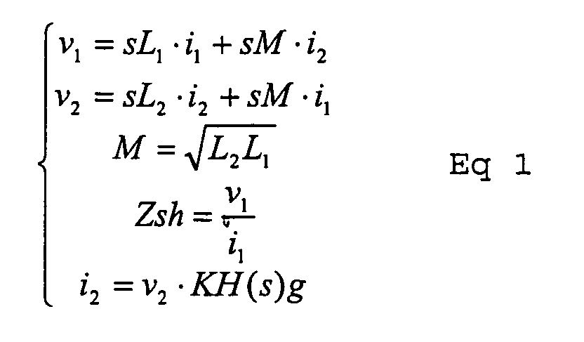
- As shown in Eq 1, the signal v2 (on the LV side) contains information about current flowing in the primary winding L1 (placed on the HV branch). The signal v2 is processed by the active part and is then transferred via mutual coupling (M) to the HV side, without a direct DC coupling with the line.
- In this way a bi-directional AC floating impedance is generated based on the following expression:
- Eq 2 and Eq 3 highlight that the impedance Zsh is modelled around sL1 acting on α and shaped in terms of frequency range through the transfer function H(s). In agreement with Table 1 below, the value for Alpha permits to increase, decrease or invert the sL1 impedance, depending on application.
synthesis effect on sL1 vs. conditions on alpha. Conditions on Ksh Conditions on alpha Effect on SL1 Ksh>0 Ksh>1 0< α < 1/sL 2 Incremented Ksh<1 α <0 Decremented Ksh<0 |Ksh| >1 1/sL 2 < α < 2/sL 2 Inverted + incremented module |Ksh| <1 2/sL 2 < α Inverted + decremented module - For example, by means of the condition expressed in Eq 4 a high impedance can be reached in a frequency band determined by H (s).
- The equation above is a key towards an active splitter.
- Stability can be analysed by taking the single ended case of figure 5 as a reference. Generally, both terminals A and B of the floating synthesized impedance are loaded towards ground via impedances ZA and ZB that play an important role in stability. In the situation considered the open loop gain (GOL) may extracted by cutting the path feedback at the point indicated with a cross [X] and by solving the circuit with respect the ratio vox/vix . This leads to the expression:
- From the point of view of noise, as shown in figure 6, the single ended circuit can be substituted by an equivalent circuit. This equivalent circuit is comprised of the synthesized impedance with a noise generator eno 2 connected in series.
- If eni 2 denotes the equivalent input noise at the input of the block K, then the equivalent output noise generator eno 2 depends linearly on eni 2 asClearly, the winding ratio:

- POTS & ISDN splitters represent a natural field of application for the described impedance synthesizer. In fact, both LV and HV signals flow in splitters but the filtering actions must be activated only on the LV component. In other words, splitters should be transparent for HV signals and provide high impedance for LV signals as specified in the standards already mentioned in the introductory portion of the description.
- The main drawbacks of a fully active splitter approach are:
- the presence of HV signals like DC battery (60VDC) and ring (100VRMS), which requires a dedicated and expensive HV SOI technology,
- power consumption, and
- complexity.
- For the reasons above, a splitter based on a hybrid arrangement as shown in figure 3 represents an optimum trade off in terms of performance, consumption, cost and complexity.
- Although reference will be made in the following primarily to POTS-xDSL splitter complying with the G.992.1 standard, those of skill in the art will promptly appreciate that the instant disclosure can be easily adapted to other standards or ISDN requirements.
- The active splitter described herein is based on a simple architecture comprised of a transformer T, acting as a ELF (Extremely Low Frequency) decoupler and an active part able to synthesize an impedance around L2 in a frequency range higher than the ELF range considered.
- The transformer T will 'block' the DC as well as the ring signal from L1 to L2. The supply requirements of the active-part will be determined only from the choice of the winding ratio' n and the PSD masks of the ADSL and Voice signals normally present on line.
- Figure 7 gives a simplified single-ended block schematic of a xDSL's system adapted to create a model.
- The symbols shown in figure 7 are as follows:
- Zadsl (co/cpe) are standard impedances through which the ADSL modem injects UP and DS on the loop,
- the box designated loop indicates the impedance of the test loop,
- Zpots (co/cpe) indicate the impedance that the PTSN and POTS side will present: these depend on POTS state (on/off hook, ringing, ring trip...),
- i1 is the current on the primary winding L1, which in the ADSL frequency band represents the residual current flowing from the line to POTS due to the finite impedance Zsh,
- i2 is the current on the LV winding that can be also seen as the lower limit for the stage current consumption g.
- A number of entities will now be defined in order to describe the whole system. Each of these will be discussed, analysed and adapted in connection with an xDSL-POTS splitter compliant with G.992.1.
- Synthesis factor: this is the ratio of the synthesized impedance and the physically used impedance sL1.
- A simplified version of Eq 3 is derived by setting (without losses in terms of generality), H = H 1·H2 and H 1 =1/sL2 , which yields:
- There are thus at least three strategies to realize a POTS splitter, depending on the choice of sL1:

- As the main target pursued is minimizing the splitter board space, the first choice is neglected while the third one is taken as a guideline.
- The foregoing translates into the following condition:
- Eq 9.3 and Eq 8 indicate H2 will be a high pass filter (HPF). Moreover, its choice should be done in order to implement a G.992.1 compliant filtering action. The band limitation of K and g acts by switching off the synthesis outside the ADSL band reducing power consumption outside the frequency region of interest.
- Synthesized impedance: this is the effective impedance seen around sL1 placed along the HV branch.
- Zsh determines the active splitter performance in terms of return loss, insertion loss, attenuation distortion, delay distortion, ADSL band attenuation and input impedance (see e.g. ITU-T Recommendation G.992.1 (1999): "Asymmetric Digital Subscriber Line (ADSL)").
- Current factor: this represents the ratio between the currents on the two windings and it is useful to determine the minimum current consumption of block g vs. the current flowing on the HV branch.
- Even if Ksh increases in the ADSL band, the current consumption i2 is limited because the filtering action will simultaneously reduce i1. Obviously, this is directly proportional to the transformer ratio n.
- Sensing factor: this is a useful parameter to provide the dynamic ranges of signal processed by the active chain vs. the current flowing on primary winding.
- As Zsh increases and n decreases, Ks will increase providing a greater signal on the active part. In any case, a decrement of i1, which leads to a limited signal v2, follows an increment of Ks in the ADSL band.
- Out noise factor: this is useful in order to obtain the equivalent output noise generator (see figure 6) vs. the equivalent input noise of the active chain K, H, g.

- Line noise factor: this is expressed as the ratio of the on-line injected noise to the equivalent input noise of the active chain including the elements K, H, g. Taking figure 7 again as a reference, ZA and ZB denote the impedances loading the nodes A and B, respectively.
- The above-mentioned factor has the expression in Eq 15. This indicates that a certain care is required in properly selecting the transformer ratio n, as this may multiply the noise injected into node B, which may disturb the ADSL channel.

- The arrangement described in the foregoing has been tested by taking into account the following edging conditions which consider the main transformer parasitics (leakage inductance and wire DC resistance), active blocks band limitations, and so on.
- Additionally, H(s) was considered as notionally comprised of three stages: a high pass filter (HPF), a low pass filter (LPF) and a phase adjustment filter (PAD), while the following quantitative parameters have been used.
Transformer parameters - L1=
- 20mH (primary winding) ,
- L2=
- 12mH (secondary winding),
- Rw=
- 10Ω (DC resistance for each winding) ,
- L1k=
- 20uH (Leakage inductance),
- Cpots=
- 100nF (capacitor in parallel with the PTSN side),
- With the above edging conditions a viable solution is:
- H2HPF is a second order elliptic high pass function with a cut-off frequency of 10kHz and 44dB attenuation, instead H1 is the function which compensate sL2 in equation Eq 3
- From Eq 19, the PAD filter is unitary, given that no phase correction is needed for this kind of H2HPF.
- Other topologies, again based on a transformer as the synthesis core, will now be briefly described in the following.
- A generalization of the idea previously described will be introduced first. A discussion of a different approach that use an HV capacitor follows.
- The embodiment described in the foregoing may be regarded as representative a more general topology as shown in figure 8. There, three impedances are added (Za, Zb, Zc) and three different injection points are considered (I, II, III). In that way, all possible sensing/injection combinations are realized by properly setting of the three added impedances.
- The circuit in figure 8 provides an impedance Zshx which can be expressed as:
- The impedances Zabc and Zbc are respectively defined as:
- The synthesis coefficients depend on the injection point, and they may be expressed as follows:

 or in a more generalized way:
- This represents the key point underlying the arrangement described herein, namely sensing and injection have been done on the secondary winding side.
- The last approach is based on current sensing across an impedance Z placed in series with the line (see figure 9). Furthermore, capacitive decoupling allows using LV devices for circuitry connected to the secondary winding. Analyzing the circuit we obtain the equations:

- Ksh depends linearly on Alpha, while the previous solutions (Eq 25) convey a hyperbolic relationship.
- This solution exhibits a drawback with respect to the previous one due to the presence of HV capacitors and a component Z placed in series with the line but presents an advantage given by its linear behavior with alpha.
- In terms of stability, Eq 29 shows the open loop gain when terminals P and L are respectively loaded with ZP and ZL; this formula put in evidence that stability is not an issue when one/both terminals are floating.

- As indicated, the arrangement described herein exhibits a number of advantages.
- In filtering applications where HV signals are present, integration has heretofore met with serious obstacles due to taxing technology requirements and power consumption: in fact, the signal dynamics made it practically compulsory to use an HV supply for the active part, thus making design very expensive in terms of power dissipation.
- The arrangement described herein achieves a reduction in the passive components needed in filtering applications like xDSL splitter. Using LV technology to integrate active devices, provides a high density solution in terms of area and cost: for instance, a high order filter can be implemented by means of an ASIC, a single transformer plus some SMD components, in the place of a huge transformers chain, thus achieving a substantial saving in PCB space.
- Of course, without prejudice to the underlying principles of the invention, the details and embodiments may vary, also significantly, with respect to what has been described, by way of example only, without departing from the scope of the invention as defined in the claims that follow.

which represent a distributed gain,
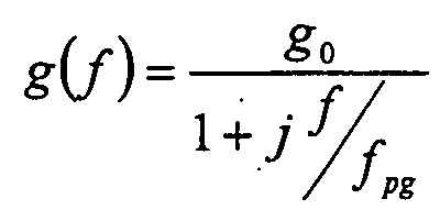
eni=100nV/√Hz (input equivalent noise of the active chain K, H, g),
Claims (19)
- An arrangement including:said impedance synthesis circuit (K, H(s), g) connected to said secondary winding (L2), whereby said transformer (T) mirrors the impedance synthesized by said impedance synthesis circuit (K, H(s),g) into said impedance (Zsh) across said primary winding (L1).a transformer (T) having a primary winding (L1) and a secondary winding (L2), the transformer exhibiting an impedance (Zsh) across said primary winding (2), andan impedance synthesis circuit (K, H(s),g) including:a transfer function element (H(s)) having a frequency spectrum, said transfer function element (H(s)) having associated a gain element (K), anda current source (g) controlled by said transfer function element (H(s)),
- The arrangement of claim 1, characterised in that said current source (g) is controlled by said transfer function element (H(s)) via a feedback path and in that said associated gain element (K) is a distributed gain over said feedback path.
- The arrangement of either of claims 1 or 2, characterised in that said current source (g) is connected to a current injection point (I, II, III) selected out of:either terminal (II, III) of said secondary winding (L2), anda point (I) connected to said secondary winding (L2) via an impedance (Zb).
- The arrangement of any of claims 1 to 3, characterised in that said transfer function element (H(s)) is connected to sense voltage at said secondary winding (L2).
- The arrangement of claim 4, characterised in that said transfer function element (H(s)) is connected to a terminal of said secondary winding (L2).
- The arrangement of either of claims 4 or 5, characterised in that said transfer function element (H(s)) is connected to said secondary winding (L2) via said gain element (K).
- The arrangement of either of claims 5 or 6, characterised in that said transfer function element (H(s)) is connected to said secondary winding (L2) via a voltage divider (Za, Zb).
- The arrangement of claim 4, characterised in that said transfer function element (H(s)) is connected for on-line sensing voltage across an impedance (Z) in series with said primary winding (L1).
- The arrangement of any of the previous claims, characterised in that said current source (g) is a voltage controlled current source (VCSS).
- The arrangement of any of the previous claims, characterised in that said transfer function element (H(s)) includes at least one filter (H2HPF, H2LPF, H2PAD) dictating said frequency spectrum.
- The arrangement of claim 10, characterised in that said transfer function element (H(s)) includes at least one high pass filter (H2HPF).
- The arrangement of either of claims 10 or 11, characterised in that said transfer function element (H(s)) includes at least one phase adjustment filter (H2PAD) .
- The arrangement of any of claims 10 to 12, characterised in that said associated gain element (K) and said current source (g) provide a low-pass filtering action, whereby said transfer function element (H(s)) is exempt from respective low pass filter elements (H2LPF) .
- The arrangement of claim 11, characterised in that said at least one high pass filter (H2HPF) is an elliptic high pass filter.
- The arrangement of any of the previous claims, characterised in that said transfer function element (H(s)) is selectively controllable to selectively modify said impedance synthesized by said impedance synthesis circuit (K, H(s), g) and mirrored into said impedance (Zsh) across said primary winding (L1).
- The arrangement of claim 15, characterised in that said transfer function element (H(s)) is selectively controllable via a digital interface.
- The arrangement of any of the previous claims, characterised in that said impedance synthesis circuit (K, H(s), g) is in the form of an integrated circuit.
- The arrangement of any of the previous claims, characterised in that said primary winding (L1) defines the high voltage (HV) side of an XDSL splitter.
- The arrangement of claims 11 and 18, characterised in that said transfer function element (H(s)) includes a high pass filter (H2HPF) implementing a high pass function with a cut-off frequency of 10kHz and 44dB attenuation.
Priority Applications (4)
| Application Number | Priority Date | Filing Date | Title |
|---|---|---|---|
| DE60311845T DE60311845D1 (en) | 2003-12-22 | 2003-12-22 | Active impedance synthesis circuit, for example for XDSL divisors |
| EP03029556A EP1549037B1 (en) | 2003-12-22 | 2003-12-22 | An active impedance synthesis circuit, for example for XDSL splitters |
| PCT/IB2004/004032 WO2005064911A1 (en) | 2003-12-22 | 2004-12-06 | An active impedance synthesis circuit, for example for xdsl splitters |
| US11/474,051 US8406391B2 (en) | 2003-12-22 | 2006-06-22 | Active impedance synthesis circuit, for example for XDSL splitters |
Applications Claiming Priority (1)
| Application Number | Priority Date | Filing Date | Title |
|---|---|---|---|
| EP03029556A EP1549037B1 (en) | 2003-12-22 | 2003-12-22 | An active impedance synthesis circuit, for example for XDSL splitters |
Publications (2)
| Publication Number | Publication Date |
|---|---|
| EP1549037A1 true EP1549037A1 (en) | 2005-06-29 |
| EP1549037B1 EP1549037B1 (en) | 2007-02-14 |
Family
ID=34530691
Family Applications (1)
| Application Number | Title | Priority Date | Filing Date |
|---|---|---|---|
| EP03029556A Expired - Lifetime EP1549037B1 (en) | 2003-12-22 | 2003-12-22 | An active impedance synthesis circuit, for example for XDSL splitters |
Country Status (4)
| Country | Link |
|---|---|
| US (1) | US8406391B2 (en) |
| EP (1) | EP1549037B1 (en) |
| DE (1) | DE60311845D1 (en) |
| WO (1) | WO2005064911A1 (en) |
Cited By (1)
| Publication number | Priority date | Publication date | Assignee | Title |
|---|---|---|---|---|
| EP1903832A1 (en) * | 2006-09-22 | 2008-03-26 | Huawei Technologies Co., Ltd. | A method and system for signal splitting and a splitter board |
Families Citing this family (1)
| Publication number | Priority date | Publication date | Assignee | Title |
|---|---|---|---|---|
| US10135626B2 (en) * | 2015-04-14 | 2018-11-20 | Avago Technologies General Ip (Singapore) Pte. Ltd. | Power coupling circuits for single-pair ethernet with automotive applications |
Citations (3)
| Publication number | Priority date | Publication date | Assignee | Title |
|---|---|---|---|---|
| DE3323651A1 (en) * | 1983-07-01 | 1985-01-17 | Standard Elektrik Lorenz Ag, 7000 Stuttgart | Circuit arrangement for increasing the shunt inductance of a transformer |
| WO1999039433A1 (en) * | 1998-01-29 | 1999-08-05 | Telefonaktiebolaget Lm Ericsson (Publ) | Active impedance converter |
| US20010045843A1 (en) * | 2000-02-29 | 2001-11-29 | Ramon Hernandez-Marti | Method and device for active impedance matching |
Family Cites Families (7)
| Publication number | Priority date | Publication date | Assignee | Title |
|---|---|---|---|---|
| US5258713A (en) * | 1992-04-16 | 1993-11-02 | Northern Telecom Limited | Impedance generator for a telephone line interface circuit |
| US5623543A (en) | 1994-02-01 | 1997-04-22 | British Telecommunications Public Limited Company | Two port signalling voltages filter arrangement |
| EP0677938A1 (en) | 1994-04-14 | 1995-10-18 | ALCATEL BELL Naamloze Vennootschap | Signal coupler |
| US5889856A (en) | 1997-05-22 | 1999-03-30 | Centillium Technology Corp. | ADSL integrated line card with digital splitter and POTS CODEC without bulky analog splitter |
| US6144735A (en) | 1998-03-12 | 2000-11-07 | Westell Technologies, Inc. | Filters for a digital subscriber line system for voice communication over a telephone line |
| ES2271983T3 (en) | 1998-06-26 | 2007-04-16 | Alcatel | PROVISION OF FILTER APPLICABLE TO ADSL SIGNAL SEPARATORS. |
| SE516523C2 (en) * | 1999-07-02 | 2002-01-22 | Ericsson Telefon Ab L M | Filter arrangement and method for filtration and impedance conversion |
-
2003
- 2003-12-22 EP EP03029556A patent/EP1549037B1/en not_active Expired - Lifetime
- 2003-12-22 DE DE60311845T patent/DE60311845D1/en not_active Expired - Lifetime
-
2004
- 2004-12-06 WO PCT/IB2004/004032 patent/WO2005064911A1/en not_active Ceased
-
2006
- 2006-06-22 US US11/474,051 patent/US8406391B2/en active Active
Patent Citations (3)
| Publication number | Priority date | Publication date | Assignee | Title |
|---|---|---|---|---|
| DE3323651A1 (en) * | 1983-07-01 | 1985-01-17 | Standard Elektrik Lorenz Ag, 7000 Stuttgart | Circuit arrangement for increasing the shunt inductance of a transformer |
| WO1999039433A1 (en) * | 1998-01-29 | 1999-08-05 | Telefonaktiebolaget Lm Ericsson (Publ) | Active impedance converter |
| US20010045843A1 (en) * | 2000-02-29 | 2001-11-29 | Ramon Hernandez-Marti | Method and device for active impedance matching |
Cited By (2)
| Publication number | Priority date | Publication date | Assignee | Title |
|---|---|---|---|---|
| EP1903832A1 (en) * | 2006-09-22 | 2008-03-26 | Huawei Technologies Co., Ltd. | A method and system for signal splitting and a splitter board |
| CN1941650B (en) * | 2006-09-22 | 2010-05-12 | 华为技术有限公司 | A signal separation method and system and separator board |
Also Published As
| Publication number | Publication date |
|---|---|
| US8406391B2 (en) | 2013-03-26 |
| WO2005064911A1 (en) | 2005-07-14 |
| DE60311845D1 (en) | 2007-03-29 |
| EP1549037B1 (en) | 2007-02-14 |
| US20070009051A1 (en) | 2007-01-11 |
Similar Documents
| Publication | Publication Date | Title |
|---|---|---|
| US6295343B1 (en) | Method and apparatus for combining voice line card and xDSL line card functions | |
| US7352776B1 (en) | Line terminator unit for a subscriber line | |
| US6748076B1 (en) | Method for separating narrowband and broadband services on a transmission link and a splitter element | |
| US20050018596A1 (en) | System for crosstalk noise reduction on twisted pair, ethernet, polyphase and shielded wire systems | |
| US6826278B2 (en) | Central office interface techniques for digital subscriber lines | |
| FI106682B (en) | Separation of narrow and broadband services during a transmission connection | |
| EP1549037B1 (en) | An active impedance synthesis circuit, for example for XDSL splitters | |
| US6978011B1 (en) | Enhanced low pass filter | |
| US6937719B2 (en) | Multiplexing and demultiplexing of narrowband and broadband services in a transmission connection | |
| US6829336B1 (en) | System and method for active filtering in a telecommunications network | |
| Zojer et al. | A broadband high-voltage SLIC for a splitter-and transformerless combined ADSL-Lite/POTS linecard | |
| EP1318653B1 (en) | Line interface for combining a voice band signal and an XDSL signal on a twisted-pair copper line | |
| US7031378B1 (en) | Unified DSL transceiver | |
| US20010033651A1 (en) | Method and apparatus for connecting broadband voice and data signals to telephone systems | |
| CA2274171A1 (en) | Loop driver for pots, xdsl, or integrated pots/xdsl interface | |
| US20020186824A1 (en) | Splitterless, transformerless, voice service independent ADSL interface | |
| US7397914B2 (en) | Multiple path hybrid for subscriber line services | |
| CN100559821C (en) | Filters for telephone lines suitable for ADSL transmission | |
| Dedieu et al. | 7th-order low-voltage CMOS POTS/ADSL splitter for DSL access multiplexer size reduction | |
| CA2383497C (en) | Method and apparatus for combining voice line card and xdsl line card functions | |
| WO1999039433A1 (en) | Active impedance converter | |
| Moons et al. | An analog telephone subscriber chipset integrating 16 lines with fully programmable central office impedance | |
| CA2375153A1 (en) | Loop driver for pots, xdsl, or integrated pots/xdsl interface | |
| CA2351242A1 (en) | Subscriber loop range extension using negative-impedance repeaters |
Legal Events
| Date | Code | Title | Description |
|---|---|---|---|
| PUAI | Public reference made under article 153(3) epc to a published international application that has entered the european phase |
Free format text: ORIGINAL CODE: 0009012 |
|
| AK | Designated contracting states |
Kind code of ref document: A1 Designated state(s): AT BE BG CH CY CZ DE DK EE ES FI FR GB GR HU IE IT LI LU MC NL PT RO SE SI SK TR |
|
| AX | Request for extension of the european patent |
Extension state: AL LT LV MK |
|
| 17P | Request for examination filed |
Effective date: 20050927 |
|
| AKX | Designation fees paid |
Designated state(s): DE FR GB IT |
|
| GRAP | Despatch of communication of intention to grant a patent |
Free format text: ORIGINAL CODE: EPIDOSNIGR1 |
|
| GRAS | Grant fee paid |
Free format text: ORIGINAL CODE: EPIDOSNIGR3 |
|
| GRAA | (expected) grant |
Free format text: ORIGINAL CODE: 0009210 |
|
| AK | Designated contracting states |
Kind code of ref document: B1 Designated state(s): DE FR GB IT |
|
| REG | Reference to a national code |
Ref country code: GB Ref legal event code: FG4D |
|
| REF | Corresponds to: |
Ref document number: 60311845 Country of ref document: DE Date of ref document: 20070329 Kind code of ref document: P |
|
| ET | Fr: translation filed | ||
| PLBE | No opposition filed within time limit |
Free format text: ORIGINAL CODE: 0009261 |
|
| STAA | Information on the status of an ep patent application or granted ep patent |
Free format text: STATUS: NO OPPOSITION FILED WITHIN TIME LIMIT |
|
| 26N | No opposition filed |
Effective date: 20071115 |
|
| PG25 | Lapsed in a contracting state [announced via postgrant information from national office to epo] |
Ref country code: DE Free format text: LAPSE BECAUSE OF FAILURE TO SUBMIT A TRANSLATION OF THE DESCRIPTION OR TO PAY THE FEE WITHIN THE PRESCRIBED TIME-LIMIT Effective date: 20070515 |
|
| PGFP | Annual fee paid to national office [announced via postgrant information from national office to epo] |
Ref country code: IT Payment date: 20071211 Year of fee payment: 5 |
|
| PGFP | Annual fee paid to national office [announced via postgrant information from national office to epo] |
Ref country code: FR Payment date: 20071228 Year of fee payment: 5 |
|
| REG | Reference to a national code |
Ref country code: FR Ref legal event code: ST Effective date: 20090831 |
|
| PG25 | Lapsed in a contracting state [announced via postgrant information from national office to epo] |
Ref country code: FR Free format text: LAPSE BECAUSE OF NON-PAYMENT OF DUE FEES Effective date: 20081231 |
|
| PG25 | Lapsed in a contracting state [announced via postgrant information from national office to epo] |
Ref country code: IT Free format text: LAPSE BECAUSE OF NON-PAYMENT OF DUE FEES Effective date: 20081222 |
|
| PGFP | Annual fee paid to national office [announced via postgrant information from national office to epo] |
Ref country code: GB Payment date: 20131125 Year of fee payment: 11 |
|
| GBPC | Gb: european patent ceased through non-payment of renewal fee |
Effective date: 20141222 |
|
| PG25 | Lapsed in a contracting state [announced via postgrant information from national office to epo] |
Ref country code: GB Free format text: LAPSE BECAUSE OF NON-PAYMENT OF DUE FEES Effective date: 20141222 |