EP1548951A1 - A regulator for impedance balancing of a transmission wire pair - Google Patents
A regulator for impedance balancing of a transmission wire pair Download PDFInfo
- Publication number
- EP1548951A1 EP1548951A1 EP03293356A EP03293356A EP1548951A1 EP 1548951 A1 EP1548951 A1 EP 1548951A1 EP 03293356 A EP03293356 A EP 03293356A EP 03293356 A EP03293356 A EP 03293356A EP 1548951 A1 EP1548951 A1 EP 1548951A1
- Authority
- EP
- European Patent Office
- Prior art keywords
- wire
- current
- signal
- basis
- coefficient
- Prior art date
- Legal status (The legal status is an assumption and is not a legal conclusion. Google has not performed a legal analysis and makes no representation as to the accuracy of the status listed.)
- Granted
Links
- 230000005540 biological transmission Effects 0.000 title claims abstract description 13
- 230000001105 regulatory effect Effects 0.000 claims abstract description 11
- 102100028680 Protein patched homolog 1 Human genes 0.000 claims description 8
- 101710161390 Protein patched homolog 1 Proteins 0.000 claims description 8
- 238000000034 method Methods 0.000 claims description 6
- 230000008878 coupling Effects 0.000 claims 1
- 238000010168 coupling process Methods 0.000 claims 1
- 238000005859 coupling reaction Methods 0.000 claims 1
- 238000012545 processing Methods 0.000 description 9
- 102100036894 Protein patched homolog 2 Human genes 0.000 description 7
- 101710161395 Protein patched homolog 2 Proteins 0.000 description 7
- 230000007423 decrease Effects 0.000 description 5
- 238000012937 correction Methods 0.000 description 3
- 230000010354 integration Effects 0.000 description 3
- 238000005070 sampling Methods 0.000 description 2
- RYGMFSIKBFXOCR-UHFFFAOYSA-N Copper Chemical compound [Cu] RYGMFSIKBFXOCR-UHFFFAOYSA-N 0.000 description 1
- 230000003321 amplification Effects 0.000 description 1
- 238000013459 approach Methods 0.000 description 1
- 229910052802 copper Inorganic materials 0.000 description 1
- 239000010949 copper Substances 0.000 description 1
- 238000001514 detection method Methods 0.000 description 1
- 238000010586 diagram Methods 0.000 description 1
- 238000003780 insertion Methods 0.000 description 1
- 230000037431 insertion Effects 0.000 description 1
- 238000003199 nucleic acid amplification method Methods 0.000 description 1
- 239000013307 optical fiber Substances 0.000 description 1
- 230000001629 suppression Effects 0.000 description 1
- 238000012546 transfer Methods 0.000 description 1
Images
Classifications
-
- H—ELECTRICITY
- H04—ELECTRIC COMMUNICATION TECHNIQUE
- H04B—TRANSMISSION
- H04B3/00—Line transmission systems
- H04B3/02—Details
- H04B3/30—Reducing interference caused by unbalanced currents in a normally balanced line
Definitions
- the present invention generally relates to the field of telephony, and more particularly without limitation, to impedance balancing of a transmission wire pair connected to a central office and a subscriber device.
- Twisted pairs of copper telephone wire have been in existence since the late nineteenth century when Alexander Graham Bell first invented them.
- most of the transmission lines in a typical telephone network commonly referred to as the telephone loop plant, are twisted pairs.
- the loop plant has been or is currently being upgraded with optical fiber, it is expected that twisted pair technology will remain in place for many years due to the high cost of upgrading and due to the ability to achieve high transmission rates over twisted pairs.
- US patent 3,989,902 shows a regulator which can be used in combination with equipment connected to a telephone type line.
- the regulator senses the amount of direct current being passed by the line and adjusts its internal AC impedance in inverse relationship thereto. This will shunt alternating current signals more severely when connected to short line loops having relatively small insertion loss, protecting a central office from excessive signal amplitudes.
- US patent 6,477,212 shows an apparatus for reducing local area and broad area interference in a twisted pair transmission system.
- the apparatus includes a detection device, such as an antenna, for example, for detecting electromagnetic interference coupled into a twisted pair line, a sampling/scaling device which samples and scales the detected signal, and a combiner device which combines a signal correction component with the signal received over the twisted pair by a differential receiver.
- the sampling/scaling device includes an analog-to-digital converter (ADC) which converts the detected analog signal into a digital signal and a digital signal processor, which receives the digital signal from the ADC and processes the signal to generate a correction signal. The correction signal is then subtracted from the signal received by the differential receiver.
- ADC analog-to-digital converter
- the present invention provides for a regulator for impedance balancing of a transmission wire pair connected to a central office and subscriber device.
- the regulator determines the average of the square values of the currents flowing through the transmission wire pair.
- the average of the square values are subtracted from each other in order to determine coefficients for regulating the currents.
- the regulator has separate feedback loops for the currents of the transmission wire pair.
- Each feedback loop has a multiplier for multiplication of a value that corresponds to the sum of the voltage levels of the two wire pairs. The resulting control signal is subtracted from the respective current.
- the invention can be used for any transmission method, such as analog telephone, ISDN, HDSL, or others.
- Figure 1 shows central office 100 of a telephone network.
- Telephone 102 or an equivalent end user device is connected to central office 100 by means of wires 104 and 106.
- Signal processing component 108 has subtracter 110, square operator 112 and integration operator 114 in order to provide a signal at its output 116 that represents the average of square value of current i1.
- Further central office 100 has signal processing component 118 for determination of a signal that represents the average of square value of current i2 that flows through wire 106.
- Signal processing component 118 has subtracter 120, square operator 122, and integration operator 124 to provide a signal that represents the average of square value of current i2 at its output 126.
- the signal processing components 118 and 126 can be implemented by separate physical components or by a single processor.
- the output signal of output 116 is substracted from the output signal of output 126 by means of subtracter 128.
- the result of the substraction is a coefficient k1.
- subtracter 130 substracts the signal of output 126 from the signal of output 116 to provide coefficient k2.
- the respective outputs of subtracters 128 and 138 can be multiplied by means of a common factor ⁇ to provide the coefficients k1 and k2, respectively.
- Adder 132 is coupled to wire 106 for sensing of voltage Ve2 and to wire 104 for sensing of voltage V'e1.
- Adder 132 has its output coupled to input of multiplier 134.
- Multiplier 134 multiplies the output of adder 132 by k1.
- Subtracter 136 subtracts the output of multiplier 134 from the voltage V"e1; V"e1 is the result of the multiplication of Ve1 with a constant coefficient . This way a feedback loop for regulating current i1 is formed.
- a corresponding feedback loop for current i2 is formed by respective adder 138, multiplier 140 and subtracter 142.
- the combined impedances of input impedance PTC1 of central office 100, impedance of wire 104, and impedance Rd of subscriber device 102 on one side and the combined impedances of PTC2, impedance of wire 106, and Rd on the other side are balanced.
- currents i1 and i2 have substantially the same value and opposite phase at all times. This has a number of advantages including common mode rejection and suppression of crosstalk.
- the averages of the square of the voltages taken on resistors (R0) located at the outputs of the access interface are measured.
- the averages of the two voltage are subtracted and the results after an amplification (k1 and k2) are delivered to a multiplier which is in charge to multiply the averages (k1 and k2) with a linear combination of the signal present on the wire of the line and the signal sent by the central office .
- the signals outgoing (k1 V1 and k2V2) are subtracted with the respective input signal.
- the amount of k1 and k2 are defined by the difference between the impedance PTC2 and PTC1 (and by extension with any difference impedance on the wire of the line).
- the behavior of the circuit can be understood as follows:
Landscapes
- Engineering & Computer Science (AREA)
- Computer Networks & Wireless Communication (AREA)
- Signal Processing (AREA)
- Cable Transmission Systems, Equalization Of Radio And Reduction Of Echo (AREA)
- Dc Digital Transmission (AREA)
Abstract
- means (108) for determining a first signal (116) being representative of an average of square value of a first current (i1) flowing through the first wire,
- means (118) for determining a second signal (126) being representative of the average of square value of a second current (i2) flowing through the second wire,
- means (128, 130) for determining first and second coefficients (k1, k2) on the basis of the first and second signals,
- first feedback means (132, 134, 136) for regulating the first current on the basis of the first coefficient,
- second feedback means (138, 140, 142) for regulating the second current on the basis of the second coefficient.
Description
- The present invention generally relates to the field of telephony, and more particularly without limitation, to impedance balancing of a transmission wire pair connected to a central office and a subscriber device.
- Twisted pairs of copper telephone wire, commonly referred to as twisted pairs, have been in existence since the late nineteenth century when Alexander Graham Bell first invented them. In fact, most of the transmission lines in a typical telephone network, commonly referred to as the telephone loop plant, are twisted pairs. Although much of the loop plant has been or is currently being upgraded with optical fiber, it is expected that twisted pair technology will remain in place for many years due to the high cost of upgrading and due to the ability to achieve high transmission rates over twisted pairs.
- US patent 3,989,902 shows a regulator which can be used in combination with equipment connected to a telephone type line. The regulator senses the amount of direct current being passed by the line and adjusts its internal AC impedance in inverse relationship thereto. This will shunt alternating current signals more severely when connected to short line loops having relatively small insertion loss, protecting a central office from excessive signal amplitudes.
- US patent 6,477,212 shows an apparatus for reducing local area and broad area interference in a twisted pair transmission system. The apparatus includes a detection device, such as an antenna, for example, for detecting electromagnetic interference coupled into a twisted pair line, a sampling/scaling device which samples and scales the detected signal, and a combiner device which combines a signal correction component with the signal received over the twisted pair by a differential receiver. The sampling/scaling device includes an analog-to-digital converter (ADC) which converts the detected analog signal into a digital signal and a digital signal processor, which receives the digital signal from the ADC and processes the signal to generate a correction signal. The correction signal is then subtracted from the signal received by the differential receiver.
- The present invention provides for a regulator for impedance balancing of a transmission wire pair connected to a central office and subscriber device. The regulator determines the average of the square values of the currents flowing through the transmission wire pair. The average of the square values are subtracted from each other in order to determine coefficients for regulating the currents.
- This has the advantage that impedance balancing can be performed with respect to both the input impedances of the central office as well as the wire impedances of the transmission wire pair. As a consequence a common mode signal component is reduced as well as crosstalk. Further the input impedances of the central office can have relatively large tolerances as those tolerances are compensated by the regulator in accordance with the present invention.
- In accordance with a preferred embodiment of the invention the regulator has separate feedback loops for the currents of the transmission wire pair. Each feedback loop has a multiplier for multiplication of a value that corresponds to the sum of the voltage levels of the two wire pairs. The resulting control signal is subtracted from the respective current.
- It is to be noted that the invention can be used for any transmission method, such as analog telephone, ISDN, HDSL, or others.
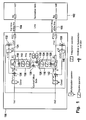
- In the following a preferred embodiment of the present invention will be described by way of example only by making reference to the drawing in which :
- Figure 1
- is a block diagram of a preferred embodiment of a central office of the invention.
- Figure 1 shows
central office 100 of a telephone network.Telephone 102 or an equivalent end user device is connected tocentral office 100 by means ofwires - Current it flows through
wire 104. The average of square value of current i1 is determined bysignal processing component 108.Signal processing component 108 has subtracter 110,square operator 112 andintegration operator 114 in order to provide a signal at itsoutput 116 that represents the average of square value of current i1. - Further
central office 100 hassignal processing component 118 for determination of a signal that represents the average of square value of current i2 that flows throughwire 106.Signal processing component 118 has subtracter 120,square operator 122, andintegration operator 124 to provide a signal that represents the average of square value of current i2 at itsoutput 126. In a practical implementation thesignal processing components - The output signal of
output 116 is substracted from the output signal ofoutput 126 by means of subtracter 128. The result of the substraction is a coefficient k1. Likewise subtracter 130 substracts the signal ofoutput 126 from the signal ofoutput 116 to provide coefficient k2. In addition the respective outputs ofsubtracters -
Adder 132 is coupled towire 106 for sensing of voltage Ve2 and to wire 104 for sensing of voltage V'e1.Adder 132 has its output coupled to input ofmultiplier 134.Multiplier 134 multiplies the output ofadder 132 by k1. Subtracter 136 subtracts the output ofmultiplier 134 from the voltage V"e1; V"e1 is the result of the multiplication of Ve1 with a constant coefficient . This way a feedback loop for regulating current i1 is formed. - A corresponding feedback loop for current i2 is formed by
respective adder 138, multiplier 140 and subtracter 142. As a result of the control of the currents i1 and i2 the combined impedances of input impedance PTC1 ofcentral office 100, impedance ofwire 104, and impedance Rd ofsubscriber device 102 on one side and the combined impedances of PTC2, impedance ofwire 106, and Rd on the other side are balanced. As a consequence currents i1 and i2 have substantially the same value and opposite phase at all times. This has a number of advantages including common mode rejection and suppression of crosstalk. - As regards the mathematical proof reference is made to mathematical appendix 1.
- The averages of the square of the voltages taken on resistors (R0) located at the outputs of the access interface are measured. The averages of the two voltage are subtracted and the results after an amplification (k1 and k2) are delivered to a multiplier which is in charge to multiply the averages (k1 and k2) with a linear combination of the signal present on the wire of the line and the signal sent by the central office . The signals outgoing (k1 V1 and k2V2) are subtracted with the respective input signal.
- The amount of k1 and k2 are defined by the difference between the impedance PTC2 and PTC1 (and by extension with any difference impedance on the wire of the line).
The behavior of the circuit (figure 1) can be understood as follows: - If ohmic value of PTC2 is lower than PTC1 then i2 is greater than i1
- Calling I1 and I2 the RMS value respectively of current i1 and i2
- If i2 is greater than i1 then 12 is greater than I1 , that involves an decrease of k1 (an increase of k2)
- If k1 decreases then k1V1 decreases
- If k1V1 decreases , Vs1 increases then
- Finally if Vs1 increases i1 increases and tends towards i2
- In the same manner with the second half loop , i2 decreases , and tends towards i1.
- The loop tends to cancel the difference between i1 and i2.
-
- Note : On figure 1 the function of multiplication of Ve1 and Ve2 by a constant (Const) allows to reduce the difference of the time transfer (delay) with k1V1 and k2V2 signals.
- This first approach could be completed by the equation of k1 and k2 . By this way we verify that the final value of k1 and k2 tend toward the equalization of the impedance and the circuit improves as foreseen , the symetrical characteristic .
From figure 1 , in taking :
By the circuit k1 = -k2 , in taking k1 = k , k2 = -k , to get K1 = K2 , the following equation must be verified (1-k2) (PTC2-PTC1) + 2k (R0 + R1) = 0
This equation has two solutions but only one is (the shortest) reached by the loop of the circuit . - Now we can verify that K1 tends towards K2 (K1 = K2).
In first estimation k = α (I1-I2) then by substituting k1 by α (I1-I2) and k2 by - α (I1-I2) in equation (i) and (ii) and from equation (e) and (ee) the RMS value of i1 and i2 are equal to:
Finally from (j) and (jj) we find : -
- 100
- Control Office
- 102
- Telephone
- 104
- Wire
- 106
- Wire
- 108
- Signal Processing Component
- 110
- Subtracter
- 112
- Square Operator
- 114
- Integration Operator
- 116
- Output of Signal Processing Component
- 118
- Signal Processing Component
- 120
- Subtracter
- 122
- Square Operator
- 124
- Information Operator
- 126
- Output of Signal Processing Component
- 128
- Subtracter
- 130
- Subtracter
- 132
- Adder
- 134
- Multiplier
- 136
- Subtracter
- 138
- Adder
- 140
- Multiplier
- 142
- Subtracter
Claims (7)
- A regulator for impedance balancing of first (104) and second wires (106) of a transmission wire pair having respective first and second impedances, the regulator comprising:means (108) for determining a first signal (116) being representative of an average of the square value of a first current (i1) flowing through the first wire,means (118) for determining a second signal (126) being representative of the average of the square value of a second current (i2) flowing through the second wire,means (128, 130) for determining first and second coefficients (k1, k2) on the basis of the first and second signals,first feedback means (132, 134, 136) for regulating the first current on the basis of the first coefficient,second feedback means (138, 140, 142) for regulating the second current on the basis of the second coefficient.
- The regulator of claim 1, the first feedback means having a first adder (132) for providing a first control signal on the basis of a voltage level of the first wire (V'e1) and a voltage level of the second wire (Ve2), a first multiplier (134) for multiplication of the first control signal with the first coefficient (k1), and a first subtracter (136) for subtracting the multiplied first control signal, and the second feedback means having a second adder (138) for providing a second control signal on the basis of a voltage level of the first wire (Ve1) and voltage level of the second wire (V'e2), and a second multiplier (140) for multiplication of the second control signal with the second coefficient (k2), and a second subtracter (142) for subtracting the multiplied second control signal.
- A central office for a telephone network, the central office having first and second input impedances (PTC1, PTC 2) for coupling of first and second wires of a transmission wire pair, the first and second wires having respective first and second impedances, the central office comprising a regulator for balancing of the combined first impedance and first input impedance and the combined second impedance and second input impedance, the regulator having:means (108) for determining a first signal (116) being representative of an average of the square value of a first current (i1) flowing through the first wire,means (118) for determining a second signal (126) being representative of the average of the square value of a second current (i2) flowing through the second wire,means (128, 130) for determining first and second coefficients (k1, k2) on the basis of the first and second signals,first feedback means (132, 134, 136) for regulating the first current on the basis of the first coefficient,second feedback means (138, 140, 142) for regulating the second current on the basis of the second coefficient.
- The central office of claim 3, the first feedback means having a first adder (132) for providing a first control signal on the basis of a voltage level of the first wire (V'e1) and a voltage level of the second wire (Ve2), a first multiplier (134) for multiplication of the first control signal with the first coefficient (k1), and a first subtracter (136) for subtracting the multiplied first control signal, and the second feedback means having a second adder (138) for providing a second control signal on the basis of a voltage level of the first wire (Ve1) and voltage level of the second wire (V'e2), and a second multiplier (140) for multiplication of the second control signal with the second coefficient (k2), and a second subtracter (142) for subtracting the multiplied second control signal.
- A method of regulating first and second currents flowing through respective first and second wires of a telephone wire pair, the method comprising:determining of a first signal being representative of the average of the square value of the first current and the second signal being representative of the average of the square value of the second current,determining of first and second coefficients on the basis of the first and second signals,regulating the first current on the basis of the first coefficient and regulating the second current on the basis of the second coefficient.
- The method of claim 5 wherein the regulation is performed by:determining first and second control signals on the basis of a voltage level of the first wire and voltage level of the second wire,multiplying of the first control signal with the first coefficient and multiplying of the second control signal with the second coefficient,subtracting of the multiplied first control signal from the first current and subtracting of the multiplied second control signal from the second current.
- The method of claim 5, wherein the first coefficient (k1) is obtained by subtracting the second signal from the first signal and wherein the second coefficient (k2) is obtained by subtracting the first signal from the second signal.
Priority Applications (3)
| Application Number | Priority Date | Filing Date | Title |
|---|---|---|---|
| AT03293356T ATE514235T1 (en) | 2003-12-26 | 2003-12-26 | ACTUATOR FOR IMPEDANCE EQUALIZATION OF A TRANSMISSION LINE |
| EP03293356A EP1548951B1 (en) | 2003-12-26 | 2003-12-26 | A regulator for impedance balancing of a transmission wire pair |
| US11/002,202 US7180998B2 (en) | 2003-12-26 | 2004-12-03 | Regulator for impedance balance of a transmission wire pair |
Applications Claiming Priority (1)
| Application Number | Priority Date | Filing Date | Title |
|---|---|---|---|
| EP03293356A EP1548951B1 (en) | 2003-12-26 | 2003-12-26 | A regulator for impedance balancing of a transmission wire pair |
Publications (2)
| Publication Number | Publication Date |
|---|---|
| EP1548951A1 true EP1548951A1 (en) | 2005-06-29 |
| EP1548951B1 EP1548951B1 (en) | 2011-06-22 |
Family
ID=34530843
Family Applications (1)
| Application Number | Title | Priority Date | Filing Date |
|---|---|---|---|
| EP03293356A Expired - Lifetime EP1548951B1 (en) | 2003-12-26 | 2003-12-26 | A regulator for impedance balancing of a transmission wire pair |
Country Status (3)
| Country | Link |
|---|---|
| US (1) | US7180998B2 (en) |
| EP (1) | EP1548951B1 (en) |
| AT (1) | ATE514235T1 (en) |
Citations (2)
| Publication number | Priority date | Publication date | Assignee | Title |
|---|---|---|---|---|
| US4387273A (en) * | 1980-08-25 | 1983-06-07 | International Telephone And Telegraph Corporation | Subscriber line interface circuit with impedance synthesizer |
| EP0467163A1 (en) * | 1990-07-06 | 1992-01-22 | Fujitsu Limited | Hybrid ciruit having a two-wire/four-wire converting function |
Family Cites Families (2)
| Publication number | Priority date | Publication date | Assignee | Title |
|---|---|---|---|---|
| EP0622943B1 (en) * | 1993-04-30 | 2001-09-12 | STMicroelectronics S.r.l. | Power management circuit for a subscriber line interface circuit |
| SE501975C2 (en) * | 1993-11-09 | 1995-07-03 | Ericsson Telefon Ab L M | Interface circuit between four-wire line and two-wire line |
-
2003
- 2003-12-26 EP EP03293356A patent/EP1548951B1/en not_active Expired - Lifetime
- 2003-12-26 AT AT03293356T patent/ATE514235T1/en not_active IP Right Cessation
-
2004
- 2004-12-03 US US11/002,202 patent/US7180998B2/en not_active Expired - Lifetime
Patent Citations (2)
| Publication number | Priority date | Publication date | Assignee | Title |
|---|---|---|---|---|
| US4387273A (en) * | 1980-08-25 | 1983-06-07 | International Telephone And Telegraph Corporation | Subscriber line interface circuit with impedance synthesizer |
| EP0467163A1 (en) * | 1990-07-06 | 1992-01-22 | Fujitsu Limited | Hybrid ciruit having a two-wire/four-wire converting function |
Also Published As
| Publication number | Publication date |
|---|---|
| US7180998B2 (en) | 2007-02-20 |
| EP1548951B1 (en) | 2011-06-22 |
| US20050142953A1 (en) | 2005-06-30 |
| ATE514235T1 (en) | 2011-07-15 |
Similar Documents
| Publication | Publication Date | Title |
|---|---|---|
| US6111949A (en) | Method of rapid automatic hybrid balancing | |
| US8300802B2 (en) | Adaptive filter for use in echo reduction | |
| EP0708537A1 (en) | Echo canceler and echo path estimating method | |
| KR19990006701A (en) | Echo Canceller with Multi-Step Gain | |
| CA1165823A (en) | Automatic equalizer for synthesizing recursive filters | |
| JPH0750553A (en) | Method of improving voice signal quality in communication channel and communication system | |
| WO1999003091A1 (en) | Methods and apparatus for measuring signal level and delay at multiple sensors | |
| US6088445A (en) | Adaptive filter system having mixed fixed point or floating point and block scale floating point operators | |
| EP0910166A2 (en) | Adaptive filter | |
| US20020159548A1 (en) | Reducing noise in a communication system | |
| US6477250B1 (en) | Adjustable hybrid having dial tone alignment configuration | |
| US20040042616A1 (en) | Echo canceling system and echo canceling method | |
| CA1168777A (en) | Digital two-to-four wire converter for full duplex signals | |
| US6782043B1 (en) | Method and apparatus for estimating the length of a transmission line | |
| US7158632B2 (en) | Adaptive scaling and echo reduction | |
| US7180998B2 (en) | Regulator for impedance balance of a transmission wire pair | |
| US5953412A (en) | Method and apparatus for controlling line conditioner equalizer | |
| US5974137A (en) | AGC amplifier for two-wire line conditioner | |
| US7016487B1 (en) | Digital echo cancellation device | |
| US6751313B2 (en) | Method and apparatus for an improved echo canceller | |
| US6891948B2 (en) | Echo canceller | |
| WO1998057502A1 (en) | Tone detection with aliasing bandpass filters | |
| CA2266277C (en) | Method and apparatus for echo control in a communication system | |
| EP0274850A2 (en) | Adaptive digital filters and echo cancelers | |
| US20070189505A1 (en) | Detecting reflections in a communication channel |
Legal Events
| Date | Code | Title | Description |
|---|---|---|---|
| PUAI | Public reference made under article 153(3) epc to a published international application that has entered the european phase |
Free format text: ORIGINAL CODE: 0009012 |
|
| 17P | Request for examination filed |
Effective date: 20041209 |
|
| AK | Designated contracting states |
Kind code of ref document: A1 Designated state(s): AT BE BG CH CY CZ DE DK EE ES FI FR GB GR HU IE IT LI LU MC NL PT RO SE SI SK TR |
|
| AX | Request for extension of the european patent |
Extension state: AL LT LV MK |
|
| AKX | Designation fees paid | ||
| RBV | Designated contracting states (corrected) |
Designated state(s): AT BE BG CH CY CZ DE DK EE ES FI FR GB GR HU IE IT LI LU MC NL PT RO SE SI SK TR |
|
| RAP1 | Party data changed (applicant data changed or rights of an application transferred) |
Owner name: ALCATEL LUCENT |
|
| 17Q | First examination report despatched |
Effective date: 20090520 |
|
| GRAP | Despatch of communication of intention to grant a patent |
Free format text: ORIGINAL CODE: EPIDOSNIGR1 |
|
| GRAS | Grant fee paid |
Free format text: ORIGINAL CODE: EPIDOSNIGR3 |
|
| GRAA | (expected) grant |
Free format text: ORIGINAL CODE: 0009210 |
|
| AK | Designated contracting states |
Kind code of ref document: B1 Designated state(s): AT BE BG CH CY CZ DE DK EE ES FI FR GB GR HU IE IT LI LU MC NL PT RO SE SI SK TR |
|
| REG | Reference to a national code |
Ref country code: GB Ref legal event code: FG4D |
|
| REG | Reference to a national code |
Ref country code: CH Ref legal event code: EP |
|
| REG | Reference to a national code |
Ref country code: IE Ref legal event code: FG4D |
|
| REG | Reference to a national code |
Ref country code: DE Ref legal event code: R096 Ref document number: 60337473 Country of ref document: DE Effective date: 20110804 |
|
| REG | Reference to a national code |
Ref country code: NL Ref legal event code: VDEP Effective date: 20110622 |
|
| PG25 | Lapsed in a contracting state [announced via postgrant information from national office to epo] |
Ref country code: SE Free format text: LAPSE BECAUSE OF FAILURE TO SUBMIT A TRANSLATION OF THE DESCRIPTION OR TO PAY THE FEE WITHIN THE PRESCRIBED TIME-LIMIT Effective date: 20110622 |
|
| PG25 | Lapsed in a contracting state [announced via postgrant information from national office to epo] |
Ref country code: SI Free format text: LAPSE BECAUSE OF FAILURE TO SUBMIT A TRANSLATION OF THE DESCRIPTION OR TO PAY THE FEE WITHIN THE PRESCRIBED TIME-LIMIT Effective date: 20110622 Ref country code: GR Free format text: LAPSE BECAUSE OF FAILURE TO SUBMIT A TRANSLATION OF THE DESCRIPTION OR TO PAY THE FEE WITHIN THE PRESCRIBED TIME-LIMIT Effective date: 20110923 Ref country code: FI Free format text: LAPSE BECAUSE OF FAILURE TO SUBMIT A TRANSLATION OF THE DESCRIPTION OR TO PAY THE FEE WITHIN THE PRESCRIBED TIME-LIMIT Effective date: 20110622 Ref country code: CY Free format text: LAPSE BECAUSE OF FAILURE TO SUBMIT A TRANSLATION OF THE DESCRIPTION OR TO PAY THE FEE WITHIN THE PRESCRIBED TIME-LIMIT Effective date: 20110622 Ref country code: AT Free format text: LAPSE BECAUSE OF FAILURE TO SUBMIT A TRANSLATION OF THE DESCRIPTION OR TO PAY THE FEE WITHIN THE PRESCRIBED TIME-LIMIT Effective date: 20110622 |
|
| PG25 | Lapsed in a contracting state [announced via postgrant information from national office to epo] |
Ref country code: NL Free format text: LAPSE BECAUSE OF FAILURE TO SUBMIT A TRANSLATION OF THE DESCRIPTION OR TO PAY THE FEE WITHIN THE PRESCRIBED TIME-LIMIT Effective date: 20110622 Ref country code: BE Free format text: LAPSE BECAUSE OF FAILURE TO SUBMIT A TRANSLATION OF THE DESCRIPTION OR TO PAY THE FEE WITHIN THE PRESCRIBED TIME-LIMIT Effective date: 20110622 |
|
| PG25 | Lapsed in a contracting state [announced via postgrant information from national office to epo] |
Ref country code: CZ Free format text: LAPSE BECAUSE OF FAILURE TO SUBMIT A TRANSLATION OF THE DESCRIPTION OR TO PAY THE FEE WITHIN THE PRESCRIBED TIME-LIMIT Effective date: 20110622 Ref country code: EE Free format text: LAPSE BECAUSE OF FAILURE TO SUBMIT A TRANSLATION OF THE DESCRIPTION OR TO PAY THE FEE WITHIN THE PRESCRIBED TIME-LIMIT Effective date: 20110622 Ref country code: PT Free format text: LAPSE BECAUSE OF FAILURE TO SUBMIT A TRANSLATION OF THE DESCRIPTION OR TO PAY THE FEE WITHIN THE PRESCRIBED TIME-LIMIT Effective date: 20111024 |
|
| RAP2 | Party data changed (patent owner data changed or rights of a patent transferred) |
Owner name: ALCATEL LUCENT |
|
| PG25 | Lapsed in a contracting state [announced via postgrant information from national office to epo] |
Ref country code: SK Free format text: LAPSE BECAUSE OF FAILURE TO SUBMIT A TRANSLATION OF THE DESCRIPTION OR TO PAY THE FEE WITHIN THE PRESCRIBED TIME-LIMIT Effective date: 20110622 Ref country code: RO Free format text: LAPSE BECAUSE OF FAILURE TO SUBMIT A TRANSLATION OF THE DESCRIPTION OR TO PAY THE FEE WITHIN THE PRESCRIBED TIME-LIMIT Effective date: 20110622 |
|
| REG | Reference to a national code |
Ref country code: CH Ref legal event code: PCOW Free format text: ALCATEL LUCENT;3, AVENUE OCTAVE GREARD;75007 PARIS (FR) |
|
| PLBE | No opposition filed within time limit |
Free format text: ORIGINAL CODE: 0009261 |
|
| STAA | Information on the status of an ep patent application or granted ep patent |
Free format text: STATUS: NO OPPOSITION FILED WITHIN TIME LIMIT |
|
| 26N | No opposition filed |
Effective date: 20120323 |
|
| PG25 | Lapsed in a contracting state [announced via postgrant information from national office to epo] |
Ref country code: IT Free format text: LAPSE BECAUSE OF FAILURE TO SUBMIT A TRANSLATION OF THE DESCRIPTION OR TO PAY THE FEE WITHIN THE PRESCRIBED TIME-LIMIT Effective date: 20110622 |
|
| PG25 | Lapsed in a contracting state [announced via postgrant information from national office to epo] |
Ref country code: DK Free format text: LAPSE BECAUSE OF FAILURE TO SUBMIT A TRANSLATION OF THE DESCRIPTION OR TO PAY THE FEE WITHIN THE PRESCRIBED TIME-LIMIT Effective date: 20110622 |
|
| REG | Reference to a national code |
Ref country code: DE Ref legal event code: R097 Ref document number: 60337473 Country of ref document: DE Effective date: 20120323 |
|
| PG25 | Lapsed in a contracting state [announced via postgrant information from national office to epo] |
Ref country code: MC Free format text: LAPSE BECAUSE OF NON-PAYMENT OF DUE FEES Effective date: 20111231 |
|
| REG | Reference to a national code |
Ref country code: CH Ref legal event code: PL |
|
| REG | Reference to a national code |
Ref country code: IE Ref legal event code: MM4A |
|
| PG25 | Lapsed in a contracting state [announced via postgrant information from national office to epo] |
Ref country code: IE Free format text: LAPSE BECAUSE OF NON-PAYMENT OF DUE FEES Effective date: 20111226 Ref country code: LI Free format text: LAPSE BECAUSE OF NON-PAYMENT OF DUE FEES Effective date: 20111231 Ref country code: CH Free format text: LAPSE BECAUSE OF NON-PAYMENT OF DUE FEES Effective date: 20111231 |
|
| PG25 | Lapsed in a contracting state [announced via postgrant information from national office to epo] |
Ref country code: ES Free format text: LAPSE BECAUSE OF FAILURE TO SUBMIT A TRANSLATION OF THE DESCRIPTION OR TO PAY THE FEE WITHIN THE PRESCRIBED TIME-LIMIT Effective date: 20111003 |
|
| PG25 | Lapsed in a contracting state [announced via postgrant information from national office to epo] |
Ref country code: LU Free format text: LAPSE BECAUSE OF NON-PAYMENT OF DUE FEES Effective date: 20111226 |
|
| PG25 | Lapsed in a contracting state [announced via postgrant information from national office to epo] |
Ref country code: BG Free format text: LAPSE BECAUSE OF FAILURE TO SUBMIT A TRANSLATION OF THE DESCRIPTION OR TO PAY THE FEE WITHIN THE PRESCRIBED TIME-LIMIT Effective date: 20110922 |
|
| PG25 | Lapsed in a contracting state [announced via postgrant information from national office to epo] |
Ref country code: TR Free format text: LAPSE BECAUSE OF FAILURE TO SUBMIT A TRANSLATION OF THE DESCRIPTION OR TO PAY THE FEE WITHIN THE PRESCRIBED TIME-LIMIT Effective date: 20110622 |
|
| PG25 | Lapsed in a contracting state [announced via postgrant information from national office to epo] |
Ref country code: HU Free format text: LAPSE BECAUSE OF FAILURE TO SUBMIT A TRANSLATION OF THE DESCRIPTION OR TO PAY THE FEE WITHIN THE PRESCRIBED TIME-LIMIT Effective date: 20110622 |
|
| REG | Reference to a national code |
Ref country code: FR Ref legal event code: GC Effective date: 20131018 |
|
| REG | Reference to a national code |
Ref country code: FR Ref legal event code: RG Effective date: 20141016 |
|
| REG | Reference to a national code |
Ref country code: FR Ref legal event code: PLFP Year of fee payment: 13 |
|
| REG | Reference to a national code |
Ref country code: FR Ref legal event code: PLFP Year of fee payment: 14 |
|
| PGFP | Annual fee paid to national office [announced via postgrant information from national office to epo] |
Ref country code: FR Payment date: 20161222 Year of fee payment: 14 |
|
| REG | Reference to a national code |
Ref country code: FR Ref legal event code: ST Effective date: 20180831 |
|
| PG25 | Lapsed in a contracting state [announced via postgrant information from national office to epo] |
Ref country code: FR Free format text: LAPSE BECAUSE OF NON-PAYMENT OF DUE FEES Effective date: 20180102 |
|
| REG | Reference to a national code |
Ref country code: GB Ref legal event code: 732E Free format text: REGISTERED BETWEEN 20190429 AND 20190502 |
|
| REG | Reference to a national code |
Ref country code: DE Ref legal event code: R082 Ref document number: 60337473 Country of ref document: DE Representative=s name: MENZIETTI WETZEL, DE Ref country code: DE Ref legal event code: R081 Ref document number: 60337473 Country of ref document: DE Owner name: PROVENANCE ASSET GROUP LLC, PITTSFORD, US Free format text: FORMER OWNER: ALCATEL LUCENT, PARIS, FR |
|
| REG | Reference to a national code |
Ref country code: GB Ref legal event code: 732E Free format text: REGISTERED BETWEEN 20220210 AND 20220216 |
|
| PGFP | Annual fee paid to national office [announced via postgrant information from national office to epo] |
Ref country code: GB Payment date: 20221228 Year of fee payment: 20 |
|
| PGFP | Annual fee paid to national office [announced via postgrant information from national office to epo] |
Ref country code: DE Payment date: 20221222 Year of fee payment: 20 |
|
| P01 | Opt-out of the competence of the unified patent court (upc) registered |
Effective date: 20230524 |
|
| REG | Reference to a national code |
Ref country code: DE Ref legal event code: R071 Ref document number: 60337473 Country of ref document: DE |
|
| REG | Reference to a national code |
Ref country code: GB Ref legal event code: PE20 Expiry date: 20231225 |
|
| PG25 | Lapsed in a contracting state [announced via postgrant information from national office to epo] |
Ref country code: GB Free format text: LAPSE BECAUSE OF EXPIRATION OF PROTECTION Effective date: 20231225 |
|
| PG25 | Lapsed in a contracting state [announced via postgrant information from national office to epo] |
Ref country code: GB Free format text: LAPSE BECAUSE OF EXPIRATION OF PROTECTION Effective date: 20231225 |