EP1548869A1 - Line converter, high-frequency module, and communication device - Google Patents
Line converter, high-frequency module, and communication device Download PDFInfo
- Publication number
- EP1548869A1 EP1548869A1 EP03791183A EP03791183A EP1548869A1 EP 1548869 A1 EP1548869 A1 EP 1548869A1 EP 03791183 A EP03791183 A EP 03791183A EP 03791183 A EP03791183 A EP 03791183A EP 1548869 A1 EP1548869 A1 EP 1548869A1
- Authority
- EP
- European Patent Office
- Prior art keywords
- line
- conductor
- dielectric substrate
- waveguide
- line converter
- Prior art date
- Legal status (The legal status is an assumption and is not a legal conclusion. Google has not performed a legal analysis and makes no representation as to the accuracy of the status listed.)
- Granted
Links
Images


Classifications
-
- H—ELECTRICITY
- H01—ELECTRIC ELEMENTS
- H01P—WAVEGUIDES; RESONATORS, LINES, OR OTHER DEVICES OF THE WAVEGUIDE TYPE
- H01P5/00—Coupling devices of the waveguide type
- H01P5/08—Coupling devices of the waveguide type for linking dissimilar lines or devices
- H01P5/10—Coupling devices of the waveguide type for linking dissimilar lines or devices for coupling balanced lines or devices with unbalanced lines or devices
- H01P5/107—Hollow-waveguide/strip-line transitions
Definitions
- the present invention relates to a line converter for a transmission line used for at least one of a microwave band and a millimeter-wave band, a high-frequency module including the line converter, and a communication device.
- an end of a micro-strip line formed as part of the plane circuit is inserted in a terminal short-circuit waveguide tube divided into two parts by a plane E of the waveguide tube.
- the two parts of the terminal short-circuit waveguide tube penetrate a groove formed in the dielectric substrate and sandwich the dielectric substrate therebetween.
- the dielectric substrate is provided at a position that is away from a short-circuit plane of a terminal short-circuit waveguide tube by as much as a predetermined distance and in a predetermined direction orthogonal to the electromagnetic-wave propagation direction.
- the dielectric substrate is provided in a predetermined direction orthogonal to the electromagnetic-wave propagation direction of the waveguide tube. Therefore, the positional relationship between the three-dimensional waveguide formed by the waveguide tube and the plane circuit formed by the dielectric substrate is determined with a low degree of flexibility. Subsequently, the plane circuit cannot be provided in a predetermined direction parallel to the electromagnetic-wave propagation direction of the waveguide tube.
- An object of the present invention is to provide a line converter wherein a plane circuit can be provided in a predetermined direction parallel to the direction in which an electromagnetic wave propagates through a three-dimensional waveguide, a dielectric substrate can be easily machined, and the characteristic of coupling between the plane circuit formed on the dielectric substrate and the three-dimensional waveguide is prevented from being affected by the precision of assembling the plane circuit and the three-dimensional waveguide so that a line-conversion characteristic according to predetermined design can be easily obtained, a high-frequency module including the line converter, and a communication device.
- the present invention provides:
- the line converter is characterized in that the dielectric substrate is provided, so as to be parallel to a plane E of the three-dimensional waveguide and at a nearly center part of the three-dimensional waveguide, and the conductor pattern of the dielectric substrate includes a conductor part forming a shield area of the three-dimensional waveguide, a coupling-line part that is electromagnetically coupled to a standing wave that occurs in the shield area, and a transmission-line part continuing from the coupling-line part.
- a standing wave required for electromagnetically coupling the three-dimensional waveguide to the transmission line on the plane circuit is generated by the shield area formed by the conductor part provided on the dielectric substrate. Therefore, the positional-relationship between the conductor part on the dielectric-substrate side forming the shield area of the three-dimensional waveguide and the coupling-line part that is electromagnetically-coupled to the standing wave generated at the shield area is determined only by the precision of forming the conductor pattern on the dielectric substrate. Subsequently, a stable coupling characteristic can be obtained without being affected by the precision of assembling the three-dimensional waveguide and the plane circuit, and a line-conversion characteristic according to predetermined design can be obtained.
- the present invention is characterized in that the conductor part forming the shield area is formed, as ground conductors formed on both faces of the dielectric substrate.
- the present invention is characterized by having a plurality of conduction paths that penetrates the dielectric substrate and that is aligned on at least one of both sides, so as to be away from the transmission line by as much as a predetermined distance, so that conduction is established between the ground conductors formed on the both faces of the dielectric substrate.
- the present invention is characterized in that a conductor of the three-dimensional waveguide is divided into two parts including an upper part and a lower part by a plane parallel to the plane E and a space is provided in the conductor of the three-dimensional waveguide, so as to create a choke by the space, where the space is provided at a position away from the three-dimensional waveguide by as much as a predetermined distance, so as to be parallel to an electromagnetic-wave propagation direction of the three-dimensional waveguide.
- the present invention is characterized by including the line converter and a high-frequency circuit connected to each of the plane circuit and the three-dimensional waveguide of the line converter.
- the present invention is characterized by forming a communication device including the high-frequency module in a unit for transmitting and receiving an electromagnetic wave.
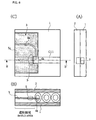
- Fig. 1 shows the configuration of the line converter.
- Fig. 1(C) is a plan view showing the line converter after an upper conductor plate 2 and an upper dielectric strip 7 are removed therefrom.
- Fig. 1(A) is an A-A' sectional view of the line converter shown in Fig. 1(C), where the upper conductor plate 2 is mounted thereon.
- Fig. 1(B) is a B-B' sectional view of the line converter shown in Fig. 1(C), where the upper conductor plate 2 is mounted thereon, as in the case of Fig. 1(A).
- reference numeral 1 denotes a lower conductor plate
- reference numeral 2 denotes the upper conductor plate
- reference numeral 3 denotes a dielectric substrate
- reference numerals 6 and 7 denote dielectric strips.
- the dielectric substrate 3 is provided, so as to be sandwiched between the lower conductor plate 1 and the upper conductor plate 2, and the dielectric strips 6 and 7.
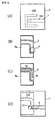
- Fig. 2 shows exploded plan views illustrating the configuration of each part of the line converter shown in Fig. 1.
- Fig. 2(A) shows the top surface of the upper conductor plate 2
- Fig. 2(B) shows the top surface of the dielectric substrate 3
- Fig. 2(C) shows a conductor pattern on the undersurface of the dielectric substrate 3
- Fig. 2(D) is a plan view of the lower conductor plate 1.
- a three-dimensional-waveguide groove G11 is provided on the lower conductor plate 1 and a three-dimensional-waveguide groove G21 is provided on the upper conductor plate 2.
- the lower dielectric strip 6 is inserted in the three-dimensional-waveguide groove G11.
- the upper dielectric strip 7 is inserted in the three-dimensional-waveguide groove G21.
- DFWG dielectric-filled waveguide
- a predetermined plane of the waveguide is determined to be a plane E (a conductor plane parallel to the electric field of a TE10 mode that is the mode of a propagating electromagnetic wave), where the plane E is parallel to the lower conductor plate 1 and the upper conductor plate 2. Therefore, the dielectric substrate 3 is provided at a position parallel to the plane E of the waveguide and corresponding to the nearly center part of the waveguide (part between the lower conductor plate 1 and the upper conductor plate 2).
- the conductor plates 1 and 2 are formed by machining a metal plate including aluminum or the like, for example. Further, the dielectric strips 6 and 7 are formed by injection-molding or machining a fluoroplastic resin.
- the dielectric substrate 3 is formed by using a ceramic substrate including aluminum or the like.
- a transmission-line conductor 4a and a coupling-line conductor 4k continuing therefrom are formed on the undersurface of the dielectric substrate 3 (the side facing the lower conductor plate 1).
- a ground conductor 5g is formed on the top surface of the dielectric substrate 3 (the side facing the upper conductor plate 2).
- the transmission-line conductor 4a formed on the dielectric substrate 3 and the ground conductor 5g formed on the surface facing the transmission-line conductor 4a form a micro-strip line.
- a notch part is formed on the ground conductor 5g on the top surface of the dielectric substrate 3, as indicated by reference character N shown in Fig. 2(B).
- the coupling-line conductor 4k facing the notch part N, the dielectric substrate 3, the lower conductor plate 1, and the upper conductor plate 2 form a suspended line.
- the transmission-line conductor 4a and the coupling-line conductor 4k are formed on the undersurface-side of the dielectric substrate 3 and the ground conductor 4g is formed in a predetermined area away from the transmission lines by as much as a predetermined distance.
- the lower conductor plate 1 has a transmission-line groove G12 that is formed thereon and along the transmission line 4a.
- the transmission-line groove G12 provides a predetermined space on the hotline side of the above-described micro-strip line and functions as a shield.
- a plurality of conduction paths (via holes) V for achieving continuity between the ground conductors 4g and 5g on the top surface and the undersurface of the dielectric substrate 3 is aligned on both sides of the transmission-line conductor 4a and the coupling-line conductor 4k, so as to be away therefrom by as much as a predetermined distance. Subsequently, unnecessary coupling between spurious mode such as parallel-flat-plate mode generated between parallel flat plates, that is, the upper and lower ground conductors 4g and 5g sandwiching the dielectric substrate 3 therebetween and micro-strip-line mode generated by the transmission-line conductor 4a and the ground conductor 5g is shielded.
- the conduction paths (via holes) V may be aligned on one side of the transmission-line conductor 4a and the coupling-line conductor 4k, so as to be away therefrom by as much as a predetermined distance.
- the dielectric substrate 3 For sandwiching the dielectric substrate 3 having various conductor patterns formed thereon between the two conductor plates 1 and 2 in the above-described manner, the dielectric substrate 3 is provided at a predetermined position with reference to the conductor plates 1 and 2 so that the coupling-line conductor 4k is inserted in the waveguide in a predetermined direction orthogonal to the electromagnetic-propagation direction of the waveguide.
- the ground conductors 4g and 5g are formed on the dielectric substrate 3 so that part of each of the ground conductors 4g and 5g is inserted in the waveguide. As shown in Fig. 1, part of the ground conductors 4g and 5g is designated by reference character S. This part forms a shield area of the waveguide.
- the waveguide is divided by the plane parallel to the plane E, whereby the shield wavelength of the waveguide is reduced and the shield area is formed in the waveguide.
- the part designated by reference character S functions as a conductor part forming the shield area relating to the present invention.
- the upper conductor plate 2 has a choke groove G22 that is parallel to the electromagnetic-wave propagation direction of the waveguide and that is away from the waveguide (from the three-dimensional-waveguide groove G21) by as much as a predetermined distance. Therefore, where the conductor plate 1 is placed on the upper conductor plate 2, a clearance generated at the interface forms a discontinuity part. However, an electromagnetic wave that is likely to leak from the clearance is released in the space of the choke groove G22.
- the distance between a part indicated by reference characters Co and a part indicated by reference characters Cs corresponds to substantially one-fourth of a propagation wavelength in Fig. 1(B)
- the part Co functions as an open end. Subsequently, the part Cs equivalently functions, as a short-circuit end. Therefore, the radiation loss generated from the clearance created by the two conductor plates 1 and 2 placed on one another hardly occurs.
- the positional relationship between the conductor part S forming the above-described shield area and the coupling-line conductor 4k depends on the dimension precision of the conductor pattern with reference to the dielectric substrate 3.
- the forming precision of the conductor pattern with reference to the dielectric substrate is significantly higher than the assembly precision of the dielectric substrate 3 with reference to the conductors 1 and 2. Therefore, the relative position of a standing wave of the three-dimensional waveguide, where the standing wave occurs by the shield area, with respect to the coupling-line conductor 4k is maintained according to predetermined design at all times. Subsequently, the characteristic of line-conversion between the waveguide and the plane circuit can be obtained according to predetermined design at all time.
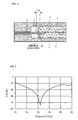
- Fig. 3 shows the result of three-dimensional electromagnetic-field analysis simulation illustrating line conversion between the waveguide and the plane circuit.
- Fig. 4 shows a cross-sectional view of the waveguide part.
- white and periodically shown patterns indicate the electric-field intensity distribution.
- ring-like patterns indicate the electric-field-intensity distribution.
- a distance Ld between the conductor part S forming the shield area and the coupling-line conductor 4k is determined so that the coupling-line conductor 4k is provided at a predetermined position where the electric-field distribution of the standing wave shows a maximum value.
- the generation of the above-described standing wave is affected by the positions of ends of the dielectric strips 6 and 7. Therefore, the distance between the ends of the dielectric strips 6 and 7, and the coupling-line conductor 4k is determined so that the coupling-line conductor 4k is provided at a position where the electric-field-intensity distribution of the standing wave shows the maximum value.
- variations in the distance between the ends of the dielectric strips 6 and 7, and the coupling-line conductor 4k exert a relatively small influence on the standing-wave generation. Therefore, the assembly precision of the dielectric strips 6 and 7, and the dielectric substrate 3 with reference to the conductor plates 1 and 2 may be low.
- the mode of the above-described suspended line is converted to the mode of the micro-strip line formed by the transmission-line conductor 4a so that electromagnetic waves are propagated in order.
- Fig. 5 shows the result of reflection characteristic S11 in the line-conversion part. As shown in this drawing, a low-reflection characteristic of under -40 dB is obtained in a 76-GHz band. Subsequently, it becomes possible to provide a line converter showing high line-conversion efficiency.
- the line converter according to the second embodiment performs line conversion between a hollow rectangular waveguide tube and a plane circuit.
- Fig. 6(C) is a plan view of the line converter after an upper conductor plate is removed therefrom.
- Fig. 6(A) is a right-side elevational view of the line converter, where the upper conductor plate is mounted thereon, and
- Fig. 6(B) is a sectional view of a B-B' portion of the line converter shown in Fig. 6(C), where the upper conductor plate is mounted on the line converter, as in the case of Fig. 6(A).
- reference numeral 1 denotes a lower conductor plate
- reference numeral 2 denotes the upper conductor plate
- reference numeral 3 denotes a dielectric substrate.
- the dielectric substrate 3 is provided, so as to be sandwiched between the lower conductor plate 1 and the upper conductor plate 2.
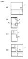
- Fig. 7 shows exploded plan views illustrating the configuration of each part of the line converter.
- Fig. 7(A) shows the top surface of the upper conductor plate 2
- Fig. 7(B) shows the top surface of the dielectric substrate 3
- Fig. 7(C) shows a conductor pattern on the undersurface side of the dielectric substrate 3
- Fig. 7(D) is a plan view of the lower conductor plate 1.
- a three-dimensional-waveguide groove G11 is provided on the lower conductor plate 1 and a three-dimensional-waveguide groove G21 is provided on the upper conductor plate 2.
- the two three-dimensional-waveguide grooves are opposed to each other. Subsequently, the hollow rectangular waveguide tube (hereinafter simply referred to as a "waveguide tube”) is formed.
- the waveguide tube has a pass-through configuration in predetermined areas shown in Figs. 6 and 7 so that no dielectric material is filled therein.
- a predetermined plane of the waveguide tube is determined to be a plane E (a conductor plane parallel to the electric field of a TE10 mode that is the mode of a propagating electromagnetic wave), where the plane E is parallel to the lower conductor plate 1 and the upper conductor plate 2. Therefore, the dielectric substrate 3 is provided at a position that is parallel to the plane E of the waveguide tube and that corresponds to the nearly center part of the waveguide tube (a part between the lower conductor plate 1 and the upper conductor plate 2).
- a transmission-line conductor 4a and a coupling-line conductor 4k continuing therefrom are formed on the undersurface of the dielectric substrate 3 (the side facing the lower conductor plate 1).
- a ground conductor 5g is formed on the top surface of the dielectric substrate 3 (the side facing the upper conductor plate 2).
- the transmission-line conductor 4a formed on the dielectric substrate 3 and the ground conductor 5g formed on the plane facing the transmission-line conductor 4a form a micro-strip line.
- the ground conductor 5g is formed only on the top-surface side of the dielectric substrate 3.
- a notch part is formed on the ground conductor 5g, as indicated by reference character N shown in Fig. 2(B).
- the coupling-line conductor 4k facing the notch part N, the dielectric substrate 3, the lower conductor plate 1, and the upper conductor plate 2 form a suspended line.
- the dielectric substrate 3 is sandwiched between the two conductor plates 1 and 2, as is the case with the first embodiment, the dielectric substrate 3 is provided at a predetermined position with reference to the conductor plates 1 and 2 so that the coupling-line conductor 4k is inserted in the waveguide in a predetermined direction orthogonal to the electromagnetic-wave-propagation direction of the waveguide tube.
- the dielectric substrate 3 is provided at a predetermined position so that the ground conductor 5g is inserted in the nearly center part of the waveguide tube, so as to be parallel to the plane E.
- a waveguide-shield area of the waveguide is formed by predetermined part designated by reference character S shown in Fig. 6 of the ground conductor 5g.
- the part indicated by reference character S is a conductor part forming the shield area.
- the coupling-line conductor, the transmission-line conductor, and the ground conductors are formed on the surfaces of the dielectric substrate 3.
- part of or all the conductors may be formed inside the dielectric substrate (internal layers).
- the dielectric-filled waveguide is used in the first embodiment, as the three-dimensional waveguide, and the hollow waveguide tube is used in the second embodiment, as the three-dimensional waveguide.
- a dielectric line including a dielectric strip sandwiched between parallel conductor planes may be formed.
- a non-radiative dielectric line may be formed.
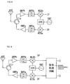
- Fig. 8 is a block diagram showing the configuration of the high-frequency module.
- reference characters ANT denote a transmission/reception antenna
- reference characters Cir denote a circulator
- each of reference characters BPFa and BPFb denotes a band-pass filter
- each of reference characters AMPa and AMPb denotes an amplifier circuit
- each of reference characters MIXa and MIXb denotes a mixer
- reference characters OSC denote an oscillator
- reference characters SYN denote a synthesizer
- reference characters IF denote an intermediate-frequency signal.
- the MIXa mixes an input IF signal and a signal output from the SYN, the BPFa makes only a predetermined signal of the mixed output signals transmitted from the MIXa pass, where the predetermined signal corresponds to a transmission-frequency band.
- the AMPa amplifies the electrical power of the signal and transmits the signal from the ANT via the Cir.
- the AMPb amplifies reception signals taken from the Cir.
- the BPFb makes only a predetermined signal of the reception signals transmitted from the AMPb pass, where the predetermined signal corresponds to a reception-frequency band.
- the MIXb mixes a frequency signal transmitted from the SYN and the reception signal, and outputs an intermediate-frequency signal IF.
- a predetermined high-frequency component including the line converter according to the first embodiment, or the second embodiment can be used, as the amplifier circuits AMPa and AMPb shown in Fig. 8. That is to say, the dielectric-filled waveguide or the hollow waveguide is used, as the transmission line, and the plane circuit including an amplifier circuit provided on the dielectric substrate is used.
- the high-frequency component including the amplifier circuits and the line converter By using the high-frequency component including the amplifier circuits and the line converter, a high-frequency module with a low loss and good communication performance is obtained.
- Fig. 9 is a block diagram showing the configuration of the communication device according to the fourth embodiment.
- the communication device includes the high-frequency module shown in Fig. 8 and a predetermined signal-processing circuit.
- the signal-processing circuit shown in Fig. 9 includes an encoding-and-decoding circuit, a synchronization-control circuit, a modulator, a demodulator, a CPU, and so forth, and further includes a circuit for inputting and outputting transmission and reception signals to and from the signal-processing circuit.
- the communication device including the high-frequency module is formed, where the high-frequency module is used, as a unit for transmitting and receiving an electromagnetic wave.
- the present invention allows forming a shield area of a three-dimensional waveguide by using a conductor pattern of a dielectric substrate. Therefore, the positional relationship between a conductor part on the dielectric-substrate side, where the conductor part forms the shield area of the three-dimensional waveguide, and a coupling-line part electromagnetically-coupled to a standing wave generated in the shield area can be determined only by the precision of forming the conductor pattern with reference to the dielectric substrate. Subsequently, it becomes possible to obtain a stable coupling characteristic and a line-conversion characteristic according to predetermined design, without being affected by the precision of assembling the three-dimensional waveguide and the plane circuit.
- the conductor part creating the shield area is formed, as ground conductors formed on both faces of the dielectric substrate. Therefore, the shielding effect of the three-dimensional waveguide increases and the size of the line converter decreases.
- conduction is established between the ground conductors by using conduction paths.
- the conduction paths are formed on at least one of both sides of the transmission line, so as to be away from the transmission line by as much as a predetermined distance and on both the faces of the dielectric substrate, so as to be provided along the transmission line. Subsequently, the coupling line and the transmission line are hardly coupled with spurious mode, so that a good spurious characteristic can be obtained.
- a space is provided in the conductor of the three-dimensional waveguide, so as to form a choke, where the space is provided at a predetermined distance from the three-dimensional waveguide, so as to be parallel to the electromagnetic-wave propagation direction of the three-dimensional waveguide. Subsequently, where the two conductor plates are joined together and the three-dimensional waveguide is formed, the radiated electrical-power loss of the three-dimensional waveguide decreases.
- the present invention provides a low-loss high-frequency module including a line converter and a high-frequency circuit connected to a plane circuit and a three-dimensional waveguide of the line converter.
- the present invention provides a communication device with decreased losses caused by line conversion and a suitable communication characteristic.
- the line converter of the present invention the characteristic of coupling between the plane circuit and the three-dimensional waveguide that are formed on the dielectric substrate is not affected by the precision of assembling the plane circuit and the three-dimensional waveguide so that a line-conversion characteristic according to predetermined design can be easily obtained. Therefore, the line converter can be used for a high-frequency module and a communication device used for at least one of a microwave band and a millimeter-wave band, for example.
Landscapes
- Waveguides (AREA)
- Waveguide Connection Structure (AREA)
- Input Circuits Of Receivers And Coupling Of Receivers And Audio Equipment (AREA)
- Control Of Motors That Do Not Use Commutators (AREA)
- Data Exchanges In Wide-Area Networks (AREA)
- Filters And Equalizers (AREA)
Abstract
Description
the conductor pattern of the dielectric substrate includes a conductor part forming a shield area of the three-dimensional waveguide, a coupling-line part that is electromagnetically coupled to a standing wave that occurs in the shield area, and a transmission-line part continuing from the coupling-line part.
The design circumstances are as follows.
Claims (11)
- A line converter including a three-dimensional waveguide for propagating an electromagnetic wave in a three-dimensional space and a plane circuit having a predetermined conductor pattern formed on a dielectric substrate, the line converter being characterized in that the dielectric substrate is provided, so as to be parallel to a plane E of the three-dimensional waveguide and at a nearly center part of the three-dimensional waveguide and the conductor pattern of the dielectric substrate includes a conductor part forming a shield area of the three-dimensional waveguide, a coupling-line part that is electromagnetically coupled to a standing wave that occurs in the shield area, and a transmission-line part continuing from the coupling-line part.
- The line converter according to Claim 1, the line converter being characterized in that the conductor part is formed, as ground conductors formed on both faces of the dielectric substrate.
- The line converter according to Claim 2, the line converter being characterized by having a plurality of conduction paths that penetrates the dielectric substrate and that is aligned on at least one of both sides of the transmission line, so as to be away from the transmission line by as much as a predetermined distance, so that conduction is established between the ground conductors formed on the both faces of the dielectric substrate.
- The line converter according to Claim 1, Claim 2, or Claim 3, the line converter being characterized in that a conductor of the three-dimensional waveguide is divided into two parts including an upper part and a lower part by a plane parallel to the plane E and a space is provided in the conductor of the three-dimensional waveguide, so as to create a choke by the space, where the space is provided at a position away from the three-dimensional waveguide by as much as a predetermined distance, so as to be parallel to an electromagnetic-wave propagation direction of the three-dimensional waveguide.
- The line converter according to Claim 1, Claim 2, or Claim 3, the line converter being characterized in that the transmission-line part is formed, as a micro-strip line including the ground conductor formed on one of the faces of the dielectric substrate and a line conductor formed on the face opposing thereto and the coupling-line part is formed, as a suspended line including the line conductor formed on one of the faces of the dielectric substrate and the conductor of the three-dimensional waveguide.
- A high-frequency module including the line converter according to Claim 1, Claim 2, or Claim 3 and a high-frequency circuit connected to each of the plane circuit and the three-dimensional waveguide of the line converter.
- A high-frequency module including the line converter according to Claim 4 and a high-frequency circuit connected to each of the plane circuit and the three-dimensional waveguide of the line converter.
- A high-frequency module including the line converter according to Claim 5 and a high-frequency circuit connected to each of the plane circuit and the three-dimensional waveguide of the line converter.
- A communication device including the high-frequency module according to Claim 6 in a unit for transmitting and receiving an electromagnetic wave.
- A communication device including the high-frequency module according to Claim 7 in a unit for transmitting and receiving an electromagnetic wave.
- A communication device including the high-frequency module according to Claim 8 in a unit for transmitting and receiving an electromagnetic wave.
Applications Claiming Priority (5)
| Application Number | Priority Date | Filing Date | Title |
|---|---|---|---|
| JP2002247556 | 2002-08-27 | ||
| JP2002247556 | 2002-08-27 | ||
| JP2003193156 | 2003-07-07 | ||
| JP2003193156A JP3975978B2 (en) | 2002-08-27 | 2003-07-07 | Line converter, high-frequency module, and communication device |
| PCT/JP2003/009420 WO2004021505A1 (en) | 2002-08-27 | 2003-07-25 | Line converter, high-frequency module, and communication device |
Publications (3)
| Publication Number | Publication Date |
|---|---|
| EP1548869A1 true EP1548869A1 (en) | 2005-06-29 |
| EP1548869A4 EP1548869A4 (en) | 2005-09-21 |
| EP1548869B1 EP1548869B1 (en) | 2009-02-18 |
Family
ID=31980487
Family Applications (1)
| Application Number | Title | Priority Date | Filing Date |
|---|---|---|---|
| EP03791183A Expired - Lifetime EP1548869B1 (en) | 2002-08-27 | 2003-07-25 | Line converter, high-frequency module, and communication device |
Country Status (9)
| Country | Link |
|---|---|
| US (1) | US7253698B2 (en) |
| EP (1) | EP1548869B1 (en) |
| JP (1) | JP3975978B2 (en) |
| KR (1) | KR100611485B1 (en) |
| AT (1) | ATE423401T1 (en) |
| AU (1) | AU2003255158A1 (en) |
| DE (1) | DE60326253D1 (en) |
| TW (1) | TWI244235B (en) |
| WO (1) | WO2004021505A1 (en) |
Cited By (1)
| Publication number | Priority date | Publication date | Assignee | Title |
|---|---|---|---|---|
| CN111988974A (en) * | 2020-07-10 | 2020-11-24 | 西安电子科技大学 | A grooved non-contact electromagnetic shielding structure, design method and application |
Families Citing this family (7)
| Publication number | Priority date | Publication date | Assignee | Title |
|---|---|---|---|---|
| US7233216B2 (en) | 2003-08-19 | 2007-06-19 | Murata Manufacturing Co., Ltd. | Line transition having a notch in the dielectric substrate adjacent the coupling line pattern |
| JP4687714B2 (en) * | 2005-08-25 | 2011-05-25 | 株式会社村田製作所 | Line converter, high-frequency module, and communication device |
| JP4345850B2 (en) | 2006-09-11 | 2009-10-14 | ソニー株式会社 | Communication system and communication apparatus |
| JP4794616B2 (en) * | 2008-11-28 | 2011-10-19 | 日本ピラー工業株式会社 | Waveguide / stripline converter |
| JP6104672B2 (en) * | 2013-03-29 | 2017-03-29 | モレックス エルエルシー | High frequency transmission equipment |
| US9490518B1 (en) * | 2015-09-28 | 2016-11-08 | Texas Instruments Incorporated | System for launching a signal into a dielectric waveguide |
| WO2019053823A1 (en) * | 2017-09-13 | 2019-03-21 | 三菱電機株式会社 | Dielectric filter |
Family Cites Families (11)
| Publication number | Priority date | Publication date | Assignee | Title |
|---|---|---|---|---|
| DE3019523C2 (en) | 1980-05-22 | 1985-05-23 | ANT Nachrichtentechnik GmbH, 7150 Backnang | Transition from a waveguide to a microstrip line |
| DE3217945A1 (en) * | 1982-05-13 | 1984-02-02 | ANT Nachrichtentechnik GmbH, 7150 Backnang | TRANSITION FROM A WAVE LADDER TO A MICROSTRIP LINE |
| JPS60192401A (en) | 1984-03-14 | 1985-09-30 | Hitachi Ltd | Microwave circuit device |
| JP3169972B2 (en) | 1991-02-26 | 2001-05-28 | 株式会社東芝 | Waveguide-microstrip line converter |
| JP3045046B2 (en) * | 1995-07-05 | 2000-05-22 | 株式会社村田製作所 | Non-radiative dielectric line device |
| JP3383542B2 (en) | 1997-01-29 | 2003-03-04 | 京セラ株式会社 | Coupling structure of dielectric waveguide line |
| JP3498597B2 (en) * | 1998-10-22 | 2004-02-16 | 株式会社村田製作所 | Dielectric line conversion structure, dielectric line device, directional coupler, high frequency circuit module, and transmission / reception device |
| JP2001111310A (en) | 1999-10-12 | 2001-04-20 | Fujitsu Ten Ltd | Structure of millimeter wave unit |
| JP4224909B2 (en) | 1999-12-02 | 2009-02-18 | 株式会社村田製作所 | Line conversion structure, high-frequency circuit, and wireless device |
| JP2002135012A (en) | 2000-10-27 | 2002-05-10 | Murata Mfg Co Ltd | Coupler, antenna device, phase shifter, antenna power measuring jig, and radar equipment |
| JP2003133815A (en) | 2001-10-22 | 2003-05-09 | Alps Electric Co Ltd | Coaxial waveguide converter |
-
2003
- 2003-07-07 JP JP2003193156A patent/JP3975978B2/en not_active Expired - Fee Related
- 2003-07-11 TW TW092118940A patent/TWI244235B/en not_active IP Right Cessation
- 2003-07-25 KR KR1020057003077A patent/KR100611485B1/en not_active Expired - Fee Related
- 2003-07-25 EP EP03791183A patent/EP1548869B1/en not_active Expired - Lifetime
- 2003-07-25 AT AT03791183T patent/ATE423401T1/en not_active IP Right Cessation
- 2003-07-25 AU AU2003255158A patent/AU2003255158A1/en not_active Abandoned
- 2003-07-25 WO PCT/JP2003/009420 patent/WO2004021505A1/en not_active Ceased
- 2003-07-25 US US10/526,105 patent/US7253698B2/en not_active Expired - Fee Related
- 2003-07-25 DE DE60326253T patent/DE60326253D1/en not_active Expired - Lifetime
Cited By (1)
| Publication number | Priority date | Publication date | Assignee | Title |
|---|---|---|---|---|
| CN111988974A (en) * | 2020-07-10 | 2020-11-24 | 西安电子科技大学 | A grooved non-contact electromagnetic shielding structure, design method and application |
Also Published As
| Publication number | Publication date |
|---|---|
| TWI244235B (en) | 2005-11-21 |
| KR100611485B1 (en) | 2006-08-09 |
| US20050285694A1 (en) | 2005-12-29 |
| JP2004147291A (en) | 2004-05-20 |
| ATE423401T1 (en) | 2009-03-15 |
| KR20050058477A (en) | 2005-06-16 |
| EP1548869B1 (en) | 2009-02-18 |
| WO2004021505A1 (en) | 2004-03-11 |
| AU2003255158A1 (en) | 2004-03-19 |
| TW200403884A (en) | 2004-03-01 |
| EP1548869A4 (en) | 2005-09-21 |
| DE60326253D1 (en) | 2009-04-02 |
| US7253698B2 (en) | 2007-08-07 |
| JP3975978B2 (en) | 2007-09-12 |
Similar Documents
| Publication | Publication Date | Title |
|---|---|---|
| KR101089195B1 (en) | Input / output coupling structure of dielectric waveguide | |
| US6868258B2 (en) | Structure for connecting non-radiative dielectric waveguide and metal waveguide, millimeter wave transmitting/receiving module and millimeter wave transmitter/receiver | |
| EP1548869B1 (en) | Line converter, high-frequency module, and communication device | |
| KR100431146B1 (en) | Transmission line connection structure, high frequency module, and communication device | |
| JP2004201163A (en) | Connection structure between cavity waveguide and dielectric waveguide | |
| EP1318563B1 (en) | Transmission line and transceiver | |
| US7535314B2 (en) | Line transition device, high-frequency module, and communication apparatus | |
| KR100435811B1 (en) | Non-radiative hybrid dielectric line transition and apparatus incorporating the same | |
| CN118920049A (en) | Four-way power division filter with medium substrate loaded in waveguide | |
| CN100490246C (en) | Line converter, high-frequency module and communication device | |
| CN117712658A (en) | Conversion device from substrate integrated waveguide to rectangular waveguide | |
| JP3838271B2 (en) | Line converter, high-frequency module, and method of manufacturing line converter | |
| EP1154511A2 (en) | Adjusting method for electrical characteristics of microstrip line filter, duplexer, communication device, and microstrip line type resonator | |
| US12148973B2 (en) | Device for transmitting a signal to a waveguide | |
| JP2007053440A (en) | Suspended stripline device and transmitting/receiving apparatus | |
| JP2002217613A (en) | Transmission line, integrated circuit and transmitting/ receiving device | |
| EP1328040B1 (en) | Transmission line and transmitter-receiver | |
| WO2020235054A1 (en) | Converter and antenna device | |
| JP2004032800A (en) | NRD Guide |
Legal Events
| Date | Code | Title | Description |
|---|---|---|---|
| PUAI | Public reference made under article 153(3) epc to a published international application that has entered the european phase |
Free format text: ORIGINAL CODE: 0009012 |
|
| 17P | Request for examination filed |
Effective date: 20050223 |
|
| AK | Designated contracting states |
Kind code of ref document: A1 Designated state(s): AT BE BG CH CY CZ DE DK EE ES FI FR GB GR HU IE IT LI LU MC NL PT RO SE SI SK TR |
|
| AX | Request for extension of the european patent |
Extension state: AL LT LV MK |
|
| A4 | Supplementary search report drawn up and despatched |
Effective date: 20050808 |
|
| DAX | Request for extension of the european patent (deleted) | ||
| 17Q | First examination report despatched |
Effective date: 20060824 |
|
| RAP1 | Party data changed (applicant data changed or rights of an application transferred) |
Owner name: MURATA MANUFACTURING CO., LTD. |
|
| GRAP | Despatch of communication of intention to grant a patent |
Free format text: ORIGINAL CODE: EPIDOSNIGR1 |
|
| GRAS | Grant fee paid |
Free format text: ORIGINAL CODE: EPIDOSNIGR3 |
|
| GRAA | (expected) grant |
Free format text: ORIGINAL CODE: 0009210 |
|
| AK | Designated contracting states |
Kind code of ref document: B1 Designated state(s): AT BE BG CH CY CZ DE DK EE ES FI FR GB GR HU IE IT LI LU MC NL PT RO SE SI SK TR |
|
| REG | Reference to a national code |
Ref country code: GB Ref legal event code: FG4D |
|
| REG | Reference to a national code |
Ref country code: CH Ref legal event code: EP |
|
| REG | Reference to a national code |
Ref country code: IE Ref legal event code: FG4D |
|
| REF | Corresponds to: |
Ref document number: 60326253 Country of ref document: DE Date of ref document: 20090402 Kind code of ref document: P |
|
| PG25 | Lapsed in a contracting state [announced via postgrant information from national office to epo] |
Ref country code: NL Free format text: LAPSE BECAUSE OF FAILURE TO SUBMIT A TRANSLATION OF THE DESCRIPTION OR TO PAY THE FEE WITHIN THE PRESCRIBED TIME-LIMIT Effective date: 20090218 Ref country code: FI Free format text: LAPSE BECAUSE OF FAILURE TO SUBMIT A TRANSLATION OF THE DESCRIPTION OR TO PAY THE FEE WITHIN THE PRESCRIBED TIME-LIMIT Effective date: 20090218 Ref country code: ES Free format text: LAPSE BECAUSE OF FAILURE TO SUBMIT A TRANSLATION OF THE DESCRIPTION OR TO PAY THE FEE WITHIN THE PRESCRIBED TIME-LIMIT Effective date: 20090529 Ref country code: SI Free format text: LAPSE BECAUSE OF FAILURE TO SUBMIT A TRANSLATION OF THE DESCRIPTION OR TO PAY THE FEE WITHIN THE PRESCRIBED TIME-LIMIT Effective date: 20090218 |
|
| NLV1 | Nl: lapsed or annulled due to failure to fulfill the requirements of art. 29p and 29m of the patents act | ||
| PG25 | Lapsed in a contracting state [announced via postgrant information from national office to epo] |
Ref country code: SE Free format text: LAPSE BECAUSE OF FAILURE TO SUBMIT A TRANSLATION OF THE DESCRIPTION OR TO PAY THE FEE WITHIN THE PRESCRIBED TIME-LIMIT Effective date: 20090518 Ref country code: AT Free format text: LAPSE BECAUSE OF FAILURE TO SUBMIT A TRANSLATION OF THE DESCRIPTION OR TO PAY THE FEE WITHIN THE PRESCRIBED TIME-LIMIT Effective date: 20090218 |
|
| PG25 | Lapsed in a contracting state [announced via postgrant information from national office to epo] |
Ref country code: BE Free format text: LAPSE BECAUSE OF FAILURE TO SUBMIT A TRANSLATION OF THE DESCRIPTION OR TO PAY THE FEE WITHIN THE PRESCRIBED TIME-LIMIT Effective date: 20090218 |
|
| PG25 | Lapsed in a contracting state [announced via postgrant information from national office to epo] |
Ref country code: CZ Free format text: LAPSE BECAUSE OF FAILURE TO SUBMIT A TRANSLATION OF THE DESCRIPTION OR TO PAY THE FEE WITHIN THE PRESCRIBED TIME-LIMIT Effective date: 20090218 Ref country code: EE Free format text: LAPSE BECAUSE OF FAILURE TO SUBMIT A TRANSLATION OF THE DESCRIPTION OR TO PAY THE FEE WITHIN THE PRESCRIBED TIME-LIMIT Effective date: 20090218 Ref country code: PT Free format text: LAPSE BECAUSE OF FAILURE TO SUBMIT A TRANSLATION OF THE DESCRIPTION OR TO PAY THE FEE WITHIN THE PRESCRIBED TIME-LIMIT Effective date: 20090727 Ref country code: DK Free format text: LAPSE BECAUSE OF FAILURE TO SUBMIT A TRANSLATION OF THE DESCRIPTION OR TO PAY THE FEE WITHIN THE PRESCRIBED TIME-LIMIT Effective date: 20090218 |
|
| PG25 | Lapsed in a contracting state [announced via postgrant information from national office to epo] |
Ref country code: SK Free format text: LAPSE BECAUSE OF FAILURE TO SUBMIT A TRANSLATION OF THE DESCRIPTION OR TO PAY THE FEE WITHIN THE PRESCRIBED TIME-LIMIT Effective date: 20090218 Ref country code: RO Free format text: LAPSE BECAUSE OF FAILURE TO SUBMIT A TRANSLATION OF THE DESCRIPTION OR TO PAY THE FEE WITHIN THE PRESCRIBED TIME-LIMIT Effective date: 20090218 |
|
| PLBE | No opposition filed within time limit |
Free format text: ORIGINAL CODE: 0009261 |
|
| STAA | Information on the status of an ep patent application or granted ep patent |
Free format text: STATUS: NO OPPOSITION FILED WITHIN TIME LIMIT |
|
| 26N | No opposition filed |
Effective date: 20091119 |
|
| PG25 | Lapsed in a contracting state [announced via postgrant information from national office to epo] |
Ref country code: BG Free format text: LAPSE BECAUSE OF FAILURE TO SUBMIT A TRANSLATION OF THE DESCRIPTION OR TO PAY THE FEE WITHIN THE PRESCRIBED TIME-LIMIT Effective date: 20090518 |
|
| PG25 | Lapsed in a contracting state [announced via postgrant information from national office to epo] |
Ref country code: MC Free format text: LAPSE BECAUSE OF NON-PAYMENT OF DUE FEES Effective date: 20090731 |
|
| REG | Reference to a national code |
Ref country code: CH Ref legal event code: PL |
|
| GBPC | Gb: european patent ceased through non-payment of renewal fee |
Effective date: 20090725 |
|
| REG | Reference to a national code |
Ref country code: FR Ref legal event code: ST Effective date: 20100331 |
|
| REG | Reference to a national code |
Ref country code: IE Ref legal event code: MM4A |
|
| PG25 | Lapsed in a contracting state [announced via postgrant information from national office to epo] |
Ref country code: LI Free format text: LAPSE BECAUSE OF NON-PAYMENT OF DUE FEES Effective date: 20090731 Ref country code: CH Free format text: LAPSE BECAUSE OF NON-PAYMENT OF DUE FEES Effective date: 20090731 Ref country code: FR Free format text: LAPSE BECAUSE OF NON-PAYMENT OF DUE FEES Effective date: 20090731 |
|
| PG25 | Lapsed in a contracting state [announced via postgrant information from national office to epo] |
Ref country code: GB Free format text: LAPSE BECAUSE OF NON-PAYMENT OF DUE FEES Effective date: 20090725 |
|
| PG25 | Lapsed in a contracting state [announced via postgrant information from national office to epo] |
Ref country code: IE Free format text: LAPSE BECAUSE OF NON-PAYMENT OF DUE FEES Effective date: 20090725 |
|
| PG25 | Lapsed in a contracting state [announced via postgrant information from national office to epo] |
Ref country code: GR Free format text: LAPSE BECAUSE OF FAILURE TO SUBMIT A TRANSLATION OF THE DESCRIPTION OR TO PAY THE FEE WITHIN THE PRESCRIBED TIME-LIMIT Effective date: 20090519 |
|
| PG25 | Lapsed in a contracting state [announced via postgrant information from national office to epo] |
Ref country code: IT Free format text: LAPSE BECAUSE OF FAILURE TO SUBMIT A TRANSLATION OF THE DESCRIPTION OR TO PAY THE FEE WITHIN THE PRESCRIBED TIME-LIMIT Effective date: 20090218 |
|
| PG25 | Lapsed in a contracting state [announced via postgrant information from national office to epo] |
Ref country code: LU Free format text: LAPSE BECAUSE OF NON-PAYMENT OF DUE FEES Effective date: 20090725 |
|
| PG25 | Lapsed in a contracting state [announced via postgrant information from national office to epo] |
Ref country code: HU Free format text: LAPSE BECAUSE OF FAILURE TO SUBMIT A TRANSLATION OF THE DESCRIPTION OR TO PAY THE FEE WITHIN THE PRESCRIBED TIME-LIMIT Effective date: 20090819 |
|
| PG25 | Lapsed in a contracting state [announced via postgrant information from national office to epo] |
Ref country code: TR Free format text: LAPSE BECAUSE OF FAILURE TO SUBMIT A TRANSLATION OF THE DESCRIPTION OR TO PAY THE FEE WITHIN THE PRESCRIBED TIME-LIMIT Effective date: 20090218 |
|
| PG25 | Lapsed in a contracting state [announced via postgrant information from national office to epo] |
Ref country code: CY Free format text: LAPSE BECAUSE OF FAILURE TO SUBMIT A TRANSLATION OF THE DESCRIPTION OR TO PAY THE FEE WITHIN THE PRESCRIBED TIME-LIMIT Effective date: 20090218 |
|
| PGFP | Annual fee paid to national office [announced via postgrant information from national office to epo] |
Ref country code: DE Payment date: 20120718 Year of fee payment: 10 |
|
| PG25 | Lapsed in a contracting state [announced via postgrant information from national office to epo] |
Ref country code: DE Free format text: LAPSE BECAUSE OF NON-PAYMENT OF DUE FEES Effective date: 20140201 |
|
| REG | Reference to a national code |
Ref country code: DE Ref legal event code: R119 Ref document number: 60326253 Country of ref document: DE Effective date: 20140201 |