EP1548814A2 - Method for producing silicon nitride films and process for fabricating semiconductor devices using said method - Google Patents
Method for producing silicon nitride films and process for fabricating semiconductor devices using said method Download PDFInfo
- Publication number
- EP1548814A2 EP1548814A2 EP04106979A EP04106979A EP1548814A2 EP 1548814 A2 EP1548814 A2 EP 1548814A2 EP 04106979 A EP04106979 A EP 04106979A EP 04106979 A EP04106979 A EP 04106979A EP 1548814 A2 EP1548814 A2 EP 1548814A2
- Authority
- EP
- European Patent Office
- Prior art keywords
- source
- silicon nitride
- film
- gas
- nitride film
- Prior art date
- Legal status (The legal status is an assumption and is not a legal conclusion. Google has not performed a legal analysis and makes no representation as to the accuracy of the status listed.)
- Withdrawn
Links
Images


Classifications
-
- H—ELECTRICITY
- H10—SEMICONDUCTOR DEVICES; ELECTRIC SOLID-STATE DEVICES NOT OTHERWISE PROVIDED FOR
- H10P—GENERIC PROCESSES OR APPARATUS FOR THE MANUFACTURE OR TREATMENT OF DEVICES COVERED BY CLASS H10
- H10P14/00—Formation of materials, e.g. in the shape of layers or pillars
- H10P14/60—Formation of materials, e.g. in the shape of layers or pillars of insulating materials
- H10P14/69—Inorganic materials
- H10P14/694—Inorganic materials composed of nitrides
- H10P14/6943—Inorganic materials composed of nitrides containing silicon
- H10P14/69433—Inorganic materials composed of nitrides containing silicon the material being a silicon nitride not containing oxygen, e.g. SixNy or SixByNz
-
- C—CHEMISTRY; METALLURGY
- C23—COATING METALLIC MATERIAL; COATING MATERIAL WITH METALLIC MATERIAL; CHEMICAL SURFACE TREATMENT; DIFFUSION TREATMENT OF METALLIC MATERIAL; COATING BY VACUUM EVAPORATION, BY SPUTTERING, BY ION IMPLANTATION OR BY CHEMICAL VAPOUR DEPOSITION, IN GENERAL; INHIBITING CORROSION OF METALLIC MATERIAL OR INCRUSTATION IN GENERAL
- C23C—COATING METALLIC MATERIAL; COATING MATERIAL WITH METALLIC MATERIAL; SURFACE TREATMENT OF METALLIC MATERIAL BY DIFFUSION INTO THE SURFACE, BY CHEMICAL CONVERSION OR SUBSTITUTION; COATING BY VACUUM EVAPORATION, BY SPUTTERING, BY ION IMPLANTATION OR BY CHEMICAL VAPOUR DEPOSITION, IN GENERAL
- C23C16/00—Chemical coating by decomposition of gaseous compounds, without leaving reaction products of surface material in the coating, i.e. chemical vapour deposition [CVD] processes
- C23C16/22—Chemical coating by decomposition of gaseous compounds, without leaving reaction products of surface material in the coating, i.e. chemical vapour deposition [CVD] processes characterised by the deposition of inorganic material, other than metallic material
- C23C16/30—Deposition of compounds, mixtures or solid solutions, e.g. borides, carbides, nitrides
- C23C16/34—Nitrides
- C23C16/345—Silicon nitride
-
- H—ELECTRICITY
- H10—SEMICONDUCTOR DEVICES; ELECTRIC SOLID-STATE DEVICES NOT OTHERWISE PROVIDED FOR
- H10P—GENERIC PROCESSES OR APPARATUS FOR THE MANUFACTURE OR TREATMENT OF DEVICES COVERED BY CLASS H10
- H10P14/00—Formation of materials, e.g. in the shape of layers or pillars
- H10P14/60—Formation of materials, e.g. in the shape of layers or pillars of insulating materials
- H10P14/63—Formation of materials, e.g. in the shape of layers or pillars of insulating materials characterised by the formation processes
- H10P14/6326—Deposition processes
- H10P14/6328—Deposition from the gas or vapour phase
- H10P14/6334—Deposition from the gas or vapour phase using decomposition or reaction of gaseous or vapour phase compounds, i.e. chemical vapour deposition
-
- H—ELECTRICITY
- H10—SEMICONDUCTOR DEVICES; ELECTRIC SOLID-STATE DEVICES NOT OTHERWISE PROVIDED FOR
- H10P—GENERIC PROCESSES OR APPARATUS FOR THE MANUFACTURE OR TREATMENT OF DEVICES COVERED BY CLASS H10
- H10P14/00—Formation of materials, e.g. in the shape of layers or pillars
- H10P14/60—Formation of materials, e.g. in the shape of layers or pillars of insulating materials
- H10P14/63—Formation of materials, e.g. in the shape of layers or pillars of insulating materials characterised by the formation processes
- H10P14/6326—Deposition processes
- H10P14/6328—Deposition from the gas or vapour phase
- H10P14/6334—Deposition from the gas or vapour phase using decomposition or reaction of gaseous or vapour phase compounds, i.e. chemical vapour deposition
- H10P14/6336—Deposition from the gas or vapour phase using decomposition or reaction of gaseous or vapour phase compounds, i.e. chemical vapour deposition in the presence of a plasma [PECVD]
-
- H—ELECTRICITY
- H10—SEMICONDUCTOR DEVICES; ELECTRIC SOLID-STATE DEVICES NOT OTHERWISE PROVIDED FOR
- H10P—GENERIC PROCESSES OR APPARATUS FOR THE MANUFACTURE OR TREATMENT OF DEVICES COVERED BY CLASS H10
- H10P14/00—Formation of materials, e.g. in the shape of layers or pillars
- H10P14/60—Formation of materials, e.g. in the shape of layers or pillars of insulating materials
- H10P14/66—Formation of materials, e.g. in the shape of layers or pillars of insulating materials characterised by the type of materials
- H10P14/668—Formation of materials, e.g. in the shape of layers or pillars of insulating materials characterised by the type of materials the materials being characterised by the deposition precursor materials
- H10P14/6681—Formation of materials, e.g. in the shape of layers or pillars of insulating materials characterised by the type of materials the materials being characterised by the deposition precursor materials the precursor containing a compound comprising Si
- H10P14/6682—Formation of materials, e.g. in the shape of layers or pillars of insulating materials characterised by the type of materials the materials being characterised by the deposition precursor materials the precursor containing a compound comprising Si the compound being a silane, e.g. disilane, methylsilane or chlorosilane
Definitions
- This invention relates to a process for producing silicon nitride films and to a process for fabricating semiconductor devices using said method .
- Monomethylamine (CH 3 NH 2 ) was selected as the nitrogen source in this study because the decomposition energy of monomethylamine (CH 3 NH 2 ) is, at 3.4 eV (CH 3 NH 2 ), less than the 4.48 eV (NH 2 -H) of ammonia (NH 3 ). The result was a reduction in the hydrogen concentration in the film to ⁇ 1 ⁇ 10 21 cm -3 at a film-formation temperature of 600°C.
- Patent Application Number 2002 - 009072 describes a method for forming silicon nitride films at 400-650°C by LPCVD using trimethylamine ((CH 3 ) 3 N, an amine-type gas) for the nitrogen source and a silane - type gas.
- this method requires that the trimethylamine ((CH 3 ) 3 N) be preheated to 500-700°C due to its high heat cap acity.
- the silicon nitride films produc ed by LPCVD exhibit a very good coverage ratio and are broadly utilized in the fabrication of transistors (MOSFETs, etc.). However, their film properties undergo deterioration (deterioration in leakage properties, increase in impurities, etc.) when their production temperature is lowered for the purpose of reducing the thermal effects on the semiconductor device.
- Silicon nitride film production at a film-formation temperature ⁇ 600°C is not accomplished in the article of Yasui et al.
- the patent application referred to hereabove due to the use of trimethylamine the required film properties cannot be obtained without preheating the gas.
- the process according to the present invention is characterized by the use for the formation of low-temperature silicon nitride film by LPCVD of ammonia (NH 3 ) as nitrogen source, monomethylamine (CH 3 NH 2 ) as the C-H bond-containing source, and Si-containing gas (e.g., monosilane (SiH 4 ), disilane (Si 2 H 6 ), dichlorosilane (SiH 2 Cl 2 ), tetrachlorosilane (SiCl 4 ), hexachlorodisilane (Si 2 Cl 6 )) as silicon source.
- NH 3 ammonia
- CH 3 NH 2 monomethylamine
- Si-containing gas e.g., monosilane (SiH 4 ), disilane (Si 2 H 6 ), dichlorosilane (SiH 2 Cl 2 ), tetrachlorosilane (SiCl 4 ), hexachlorodisilane (Si
- Disilazane (SiH 3 ) 2 NH) can also be used as a silicon source. When disilazane is used, it can be utilized not only for silicon, but also as a portion of the nitrogen source. Hydrazine (N 2 H 4 ) can also be used as a nitrogen source.
- Gas other than monomethylamine (CH 3 NH 2 ) that contains methyl in the source substance can be used, such as dimethylamine ((CH 3 ) 2 (NH)) and trimethylamine ((CH 3 ) 3 N). It is also possible to use gas that contains a non -methyl alkyl group such as ethyl, propyl, butyl, and so forth.
- th e process according to the invention is characterized by the use of at least a gas, such as monosilane, disilane, dichlorosilane, tetrachlorosilane, hexachlorodisilane, disilazane, etc. that contains at least silicon in the source substance as silicon sou rce and at least a gas such as ammonia, hydrazine, etc., that contains at least nitrogen in the source substance as nitrogen source and by the additional use of at least a gas that contains at least the carbon -hydrogen bond in the source substance.
- a gas such as monosilane, disilane, dichlorosilane, tetrachlorosilane, hexachlorodisilane, disilazane, etc. that contains at least silicon in the source substance as silicon sou rce and at least a gas such as ammonia, hydrazine, etc., that contains at least nitrogen in the source substance as nitrogen source and by the additional use of at least
- the process according to the invention is characterized by the use of gas such as monosilane, disilane, dichlorosilane, tetrachlorosilane, hexachlorodisilane, disilazane, etc. that contains at least silicon in the source substance as silicon source and at least a gas such as ammonia, hydrazine, etc. that contains at least nitrogen in the source substance as nitrogen source and by the additional use of gas that contains at least the methyl group in the source substance.
- gas such as monosilane, disilane, dichlorosilane, tetrachlorosilane, hexachlorodisilane, disilazane, etc. that contains at least silicon in the source substance as silicon source and at least a gas such as ammonia, hydrazine, etc. that contains at least nitrogen in the source substance as nitrogen source and by the additional use of gas that contains at least the methyl group in the source substance.
- the process according to the invention is characterized by the use of at least a gas that contains at least silicon in the source substance as silicon source and at least a gas that contains at least nitrogen in the source substance as nit rogen source and by the additional use of at least a gas that contains at least an alkyl group such as methyl, ethyl, propyl, butyl, etc. in the source substance.
- the process is furthercharacterized by the use of at least a gas that contains at least nitrogen and methyl in the source substance as nitrogen source.
- the process is characterized by the use of at least a gas that contains at least nitrogen and an alkyl group in the source substance as nitrogen source.
- the gas that contains at least a carbon-hydrogen bond in the source substance is according to a first embodiment a gas that contains at least nitrogen and methyl in the source substance, and according to a second embodiment a gas that contains at least nitrogen and alkyl in the source substance..
- t he gas that contains at least the carbon - hydrogen bond in the source substance comprises methylamine.
- the silicon nitride film formation is carried out by low-pressure CVD.
- silicon nitride film containing 0.7 -1.3 nitrogen where the silicon component is designated as 1, said silicon nitride film contains 0.1 -0.6 carbon.
- the invention is characterized by the use of chlorine- and silicon-containing gas comprising dichlorosilane, tetrachlorosilane, or hexachlorodisilane as the silicon source and the use of methyl - and nitrogen-containing gas comprising monomethylamine, dimethylamine, or trimethylamine as the nitrogen source.
- the invention also relates to a process for fabricating a semiconductor device in which a source region and a drain region separated by a gap are formed in a semiconductor substrate, a gate electrode is formed above the channel region that is formed in the gap between the source region and drain region wherein the gate electrode is separated from the channel region by a gate dielectric film, a source electrode is formed on the source region, a drain electrode is formed on the drain region, and sidewall film comprising silicon nitride film is formed on the sidewalls of the gate dielectric film and gate electrode, said method being characterized by the use for formation of the sidewall f ilm comprising silicon nitride of at least a gas that contains at least silicon in the source substance as silicon source and at least a gas that contains at least nitrogen in the source substance as nitrogen source and by the additional use of at least a gas that contains at least a carbon -hydrogen bond.
- the process according to the invention is characterized by the use of low - pressure CVD for formation of the silicon nitride film as wherein the silicon nitride film formation temperature is at least 450 °C but no more than 600°C.
- metal silicide film is used for the source electrode and drain electrode.
- a liner film comprising silicon nit ride film is formed on the entire surface containing this metal silicide film and the gate electrode, wherein said liner film comprising silicon nitride film is produced using low-pressure CVD, at least a gas that contains at least chlorine and silicon in the source substance as silicon source, and at least a gas that contains at least methyl and nitrogen in the source substance as nitrogen source.
- th e liner film comprising silicon nitride film is formed at a temperature of at least 450°C but no more than 600°C.
- a further embodiment of this process is characterized in that, after formation of the liner film comprising silicon nitride film, an interlay er dielectric film is formed on the liner film, the interlayer dielectric film being selectively etched over the gate electrode, source electrode, and drain electrode, and metal is filled into the etched regions.
- metal int erconnections are made on the interlayer dielectric film after metal has been filled into the etched regions , said metal interconnections being connected with the metal fill.
- the present invention carries out silicon nitride film formation at low tempera tures and thereby enables a reduction in the thermal budget from that imposed by the prior - art high-temperature production of silicon nitride films for semiconductor devices such as MOSFETs.
- this invention provides improved reliability for the electrical properties of semiconductor devices such as MOSFETs.
- application of this invention to the sidewalls of a semiconductor device can improve the leakage characteristics for this sidewall and can suppress impurity diffusion into the gate dielectric film and gate electrode encompassed by the sidewall. This results in stabilization of the electrical properties of the semiconductor device, e.g., a MOSFET.
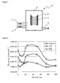
- Figure 1 illustrates an LPCVD tool for executing the method accor ding to the present invention for forming silicon nitride films.
- Silicon source (SiH 2 Cl 2 , SiCl 4 , Si 2 Cl 6 , etc.) gas is fed into this LPCVD tool 10 from the injector 11; a mixed gas of monomethylamine (CH 3 NH 2 ) and ammonia (NH 3 ) as nitrogen source is fed from the injector 12; and a silicon nitride film is formed on the silicon wafer 14 that is mounted in the boat 13 in the reaction compartment 15.
- Reference symbol 16 refers to an exhaust port.
- the addition of the monomethylamine makes it possible to terminate the silicon dangling bonds with the methyl group and thereby enables an improvement in the film quality and leakage characteristics, etc., even at low temperatures (450 -600°C). While low temperatures (450-600°C) are identified for the film -formation temperature, the film - formation temperature is not limited to these temperatures. That is, silicon nitride film with good film properties and good leakage characteristics can be obtained even at film - formation temperatures below 450°C.
- a silicon nitride film is formed on the silicon wafer 14 mounted in the boat 13 by the feed of a silicon source (Si 2 Cl 6 ) from the injector 11 and the feed of a nitrogen source (CH 3 NH 2 + NH 3 ) from the injector 12 into the LPCVD tool 10.
- a silicon source Si 2 Cl 6
- a nitrogen source CH 3 NH 2 + NH 3
- the film properties of the silicon nitride film can as a consequence be improved due to the highly efficient reaction of the CH 3 NH 2 and Si 2 Cl 6 , which are thoroughly decomposed at the film-formation temperature of 525°C.
- the film -formation conditions are not limited to the preceding, and, fo r example, temperatures of 450 -600°C, pressures of about 0.2 - 5 torr, and gas flow rate ratios (Si 2 Cl 6 flow rate/(CH 3 NH 2 + NH 3 flow rate)) of about 1/10 to 1/100 are desirable.
- This low-temperature film formation provides increased device reliability becaus e it provides an improved silicon nitride film quality without the application of excess heat to the semiconductor device during the device fabrication process.
- FIG. 2 -6 Examples of the improved film quality are illustrated in Figures 2 -6.
- Figure 2 reports the results of a determination of the SiH concentration and NH concentration in the silicon nitride film by FT -IR (Fourier-transform infrared spectroscopy) measurement.
- the SiH + NH concentration is reduced in this figure in the range of 5-20% for the ratio CH 3 NH 2 /(CH 3 NH 2 + NH 3 ) between the monomethylamine (CH 3 NH 2 ) and ammonia in the nitrogen source.
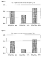
- Figure 3 contains a comparative evaluation of the integrated value over temperature of the measured intensity of the amount of H 2 O desorption from the silicon nitride film in TDS (thermal desorption gas analysis) analysis for 0%, 15%, and 25% monomethylamine (CH 3 NH 2 /(CH 3 NH 2 + NH 3 )).
- This comparative evaluation shows that 15% monomethylamine (CH 3 NH 2 ) provided less H 2 O desorption than for the heretofore used 100% ammonia (NH 3 ) (0% for the monomethylamine ratio (CH 3 NH 2 /(CH 3 NH 2 + NH 3 )), while 25% monomethylamine (CH 3 NH 2 ) provided more H 2 O desorption.
- Figure 4 contains an evaluation of the amount of HCl desorption from the silicon nitride film in TDS analysis for 0%, 15%, and 25% monomethylamine.
- This comparative evalua tion shows that 15% monomethylamine (CH 3 NH 2 ) provided less HCl desorption than for the heretofore used 100% ammonia (NH 3 ) (0% for the monomethylamine ratio), while 25% monomethylamine (CH 3 NH 2 ) provided more HCl desorption.
- Figure 5 reports the results of a determination of the IV characteristics of silicon nitride films produced on Si substrates in accordance with Figure 1.
- the leakage current density is smaller for 15% CH 3 NH 2 , 85% NH 3 from low field to high field than for the heretofore used 0% CH 3 NH 2 , 100% NH 3 .
- the leakage current density is the same at a field of 0 -1 MV/cm, an improved leakage characteristic is provided by 15% CH 3 NH 2 , 85% NH 3 at a field greater than 1 MV/cm.
- Figure 6 reports the relationship between the % monomethylamine (CH 3 NH 2 ) in the nitrogen source and the etch rate during wet etching with HF solution.
- % CH 3 NH 2 % monomethylamine
- Figure 6 reports the relationship between the % monomethylamine (CH 3 NH 2 ) in the nitrogen source and the etch rate during wet etching with HF solution.
- etch rate declines as the % CH 3 NH 2 increases. This is thought to be due to an increased resistance to etching by HF solution due to an increase in the density of the silicon nitride film generated by the carbon supplied from the CH 3 NH 2 .
- a sharp decline is noted during the increase in % CH 3 NH 2 to 25%, and the optimal range is therefore up to about 20% considering Figures 2 -5.
- Figure 7 reports experimental data taken at a film -formation temperature of 525°C.
- the carbon concentration here is about 0.1 -0.6 C : 1 Si for a nitrogen/silicon ratio in the silicon nitride film brought to 0.7 -1.3 (composition range obtained by varying the atomic ratio during CVD film formation).
- Figures 8(a) through (d) contain process cross sections that illustrate an example of the application of the inventive silicon nitride film to a MOSFET (dielectric gate transistor).
- MOSFET dielectric gate transistor
- an element isolation region 72 comprising a dielectric (e.g., SiO 2 ) is formed on a silicon substrate 71 and a MOSFET 70 is formed in the region defined by the element-forming regions.
- This MOSFET 70 is constituted of source and drain extension regions 73a, 73b (denoted below as SD extensions) that have been ion-implanted with boron (B), a source region 74a and drain region 74b corresponding to these SD extensions, and a gate electrode 77 separated by an intervening gate dielectric film 76.
- a channel region 75 is formed between the SD extensions in this MOSFET 70, while a sidewall film 78 is formed on the sidewall surfaces of the gate dielectric film 76 and gate electrode 77.
- This sidewall film 78 comprises Si 3 N 4 film and is formed using the LPCVD tool shown in Figure 1 and the production conditions given in Example 1 and a film-formation temperature around 500°C.
- the gate dielectric film under consideration frequently has a two -layer structure in which the lower layer is SiO 2 film and the upper layer is formed of a high - k film such as HfO 2 .
- the inventive silicon nitride film may be used for the lower film in these cases.
- a trilayer film may also be used in which the lower layer is SiO 2 film, the middle layer is the silicon nitride film, and the upper layer is a high -k film.
- the gate electrode surface is preferably also provided with a silicided electrode 79c .
- a silicon nitride film 80 comprising, for example, Si 3 N 4 , is formed over the entirety of the silicided gate electrode, source electrode, and drain electrode.
- This silicon nitride film 80 forms a liner film; this liner film can be formed under the sa me conditions as in Example 1 to a thickness of about 50 nm.
- a relatively thick interlayer dielectric film 81 comprising SiO 2 is formed on this liner film 80.
- this interlayer dielectric film 81 is selectively etched to form openings that are filled with metal 82. This is followed by the elaboration of interconnects 83 of, for example, aluminum, thus completing the process.
- the subject sili con nitride film can be produced by atmospheric pressure CVD or by some other technique such as, for example, plasma CVD or catalytic CVD.
- Example 2 Due to the addition in Example 2 of monomethylamine (CH 3 NH 2 ) to the film-formation source substances used for fabrica tion of the silicon nitride sidewall film, the lateral leakage at the prior-art sidewall 88 shown in Figure 9 is also eliminated and the concentrations of chlorine 86 and hydrogen 87 in the film are lowered.
- the additional use of the silicon nitride film f or the liner film can provide a stable MOSFET that is also free of surface leakage.
- use of the silicon nitride film as the lower layer in the gate dielectric film results in an extremely small source/drain leakage.
Landscapes
- Chemical & Material Sciences (AREA)
- Inorganic Chemistry (AREA)
- General Chemical & Material Sciences (AREA)
- Chemical Kinetics & Catalysis (AREA)
- Engineering & Computer Science (AREA)
- Materials Engineering (AREA)
- Mechanical Engineering (AREA)
- Metallurgy (AREA)
- Organic Chemistry (AREA)
- Formation Of Insulating Films (AREA)
- Chemical Vapour Deposition (AREA)
Abstract
Description
Japanese Laid Open (Unexamined or Kokai or A) Patent Application Number 2002 - 009072 describes a method for forming silicon nitride films at 400-650°C by LPCVD using trimethylamine ((CH 3)3N, an amine-type gas) for the nitrogen source and a silane - type gas. However, this method requires that the trimethylamine ((CH 3)3N) be preheated to 500-700°C due to its high heat cap acity. It is also stated that an insufficiently nitridated silicon nitride film (refractive index: RI = 2.9) is obtained when silicon nitride film production is carried out, for example, at 550°C, without this preheating.
In accordance with any of the three aspects of the invention hereabove disclosed, the process is characterized by the use of at least a gas that contains at least nitrogen and an alkyl group in the source substance as nitrogen source.
In accordance with the first aspect of the invention, the gas that contains at least a carbon-hydrogen bond in the source substance is according to a first embodiment a gas that contains at least nitrogen and methyl in the source substance, and according to a second embodiment a gas that contains at least nitrogen and alkyl in the source substance..
Claims (18)
- Method for forming silicon nitride film, that is characterized by the use of gas that contains at least silicon in the source substance as silicon source and gas that contains at least nitrogen in the source substance as nitrogen source and by the additional use of gas that contains at least the carbon -hydrogen bond in the source substance.
- Method for forming silicon nitride film, characterized by the use of gas that contains at least silicon in the source substance as silicon source and gas that contains at least nitrogen in the source substance as nitrogen source and by the additional use of gas that contains at least the methyl group in the source substance.
- Method for forming s ilicon nitride film, characterized by the use of gas that contains at least silicon in the source substance as silicon source and gas that contains at least nitrogen in the source substance as nitrogen source and by the additional use of gas that contains at least an alkyl group in the source substance.
- Method according to any of Claims 1 -3 for forming silicon nitride film, characterized by the use of gas that contains at least methyl and nitrogen in the source substance as nitrogen source.
- Method according to any of Claims 1 -3 for forming silicon nitride film, characterized by the use of gas that contains at least alkyl and nitrogen in the source substance as nitrogen source.
- Method for forming silicon nitride film, characterized by the use of gas that contains at least nitrogen and methyl in the source substance as the gas described in Claim 1 that contains at least the carbon -hydrogen bond in the source substance.
- Method for forming silicon nitride film, characterized by the use of gas that contains at least nitrogen and alkyl in the source substance as the gas described in Claim 1 that contains at least the carbon -hydrogen bond in the source substance.
- Method for forming silicon nitride film, characterized by the use of gas that contains at least methylamine in the source substance as the gas described in Claim 1 that contains at least the carbon -hydrogen bond in the source substance.
- Method for forming silicon nitride film, characterized in that the silicon nitride film formation described in Claims 1-8 is carried out by low-pressure CVD.
- Method for forming silicon nitride film, characterized in that, when film formation is carried out using the source substances described in Claims 1 -5 to give silicon nitride film containing 0.7-1.3 nitrogen where the silicon component is designated as 1, said silicon nitride film contains 0.1 -0.6 carbon.
- Method for forming silicon nitride film, characterized by the use of chlorine - and silicon-containing gas comprising dichlorosilane, tetrachloros ilane, or hexachlorodisilane as the silicon source described in Claim 1 and the use of methyl - and nitrogen-containing gas comprising monomethylamine, dimethylamine, or trimethylamine as nitrogen source.
- Process for fabricating a semiconductor device i n which a source region and a drain region separated by a gap are formed in a semiconductor substrate, a gate electrode is formed above the channel region that is formed in the gap between the source region and drain region wherein the gate electrode is se parated from the channel region by a gate dielectric film, a source electrode is formed on the source region, a drain electrode is formed on the drain region, and sidewall film comprising silicon nitride film is formed on the sidewalls of the gate dielectric film and gate electrode, said method being characterized by the use for formation of the sidewall film comprising silicon nitride of gas that contains at least silicon in the source substance as silicon source and gas that contains at least nitrogen in the source substance as nitrogen source and by the additional use of gas that contains at least the carbon - hydrogen bond.
- Process for fabricating a semiconductor device that characteristically uses low-pressure CVD for formation of the silicon nitride film as described in Claim 12 wherein the silicon nitride film formation temperature is at least 450°C but no more than 600°C.
- Process for fabricating a semiconductor device, characterized by the use of a metal silicide film for the source electrode an d drain electrode described in Claim 12.
- Process for fabricating a semiconductor device, characterized in that, after formation of the metal silicide film described in Claim 14, a liner film comprising silicon nitride film is formed on the entire surf ace containing this metal silicide film and the gate electrode, wherein said liner film comprising silicon nitride film is produced using low - pressure CVD, gas that contains at least chlorine and silicon in the source substance as silicon source, and gas t hat contains at least methyl and nitrogen in the source substance as nitrogen source.
- Process for fabricating a semiconductor device that characteristically uses low-pressure CVD for formation of the silicon nitride film as described in Claim 15 wherein the liner film comprising silicon nitride film is formed at a temperature of at least 450°C but no more than 600°C.
- Process for fabricating a semiconductor device, characterized in that, after formation of the liner film comprising silicon nitride f ilm as described in Claim 15, an interlayer dielectric film is formed on the liner film; the interlayer dielectric film is selectively etched over the gate electrode, source electrode, and drain electrode; and metal is filled into the etched regions.
- Process for fabricating a semiconductor device, characterized by elaborating metal interconnects on the interlayer dielectric film after metal has been filled into the etched regions as described in Claim 17 wherein the metal interconnects are connected with the metal fill.
Applications Claiming Priority (4)
| Application Number | Priority Date | Filing Date | Title |
|---|---|---|---|
| JP2003428942 | 2003-12-25 | ||
| JP2003428942 | 2003-12-25 | ||
| JP2004338459 | 2004-11-24 | ||
| JP2004338459A JP2005210076A (en) | 2003-12-25 | 2004-11-24 | Method for forming silicon nitride film and method for manufacturing semiconductor device using this method |
Publications (2)
| Publication Number | Publication Date |
|---|---|
| EP1548814A2 true EP1548814A2 (en) | 2005-06-29 |
| EP1548814A3 EP1548814A3 (en) | 2009-05-27 |
Family
ID=34554863
Family Applications (1)
| Application Number | Title | Priority Date | Filing Date |
|---|---|---|---|
| EP04106979A Withdrawn EP1548814A3 (en) | 2003-12-25 | 2004-12-24 | Method for producing silicon nitride films and process for fabricating semiconductor devices using said method |
Country Status (4)
| Country | Link |
|---|---|
| US (1) | US7351670B2 (en) |
| EP (1) | EP1548814A3 (en) |
| JP (1) | JP2005210076A (en) |
| TW (1) | TW200525642A (en) |
Cited By (3)
| Publication number | Priority date | Publication date | Assignee | Title |
|---|---|---|---|---|
| ITMI20092353A1 (en) * | 2009-12-30 | 2011-06-30 | St Microelectronics Srl | MIM CONDENSER WITH PLATE WITH HIGH MELT POINT |
| ITMI20092354A1 (en) * | 2009-12-30 | 2011-06-30 | St Microelectronics Srl | CONDENSER INTEGRATED WITH INVERTED DISHES |
| CN110205606A (en) * | 2018-02-28 | 2019-09-06 | 株式会社国际电气 | Semiconductor device manufacturing method, substrate processing apparatus, and recording medium |
Families Citing this family (43)
| Publication number | Priority date | Publication date | Assignee | Title |
|---|---|---|---|---|
| JP4279176B2 (en) * | 2004-03-02 | 2009-06-17 | 株式会社アルバック | Method for forming silicon nitride film |
| US7371649B2 (en) * | 2005-09-13 | 2008-05-13 | United Microelectronics Corp. | Method of forming carbon-containing silicon nitride layer |
| US20080124946A1 (en) * | 2006-11-28 | 2008-05-29 | Air Products And Chemicals, Inc. | Organosilane compounds for modifying dielectrical properties of silicon oxide and silicon nitride films |
| US8105925B2 (en) * | 2008-07-30 | 2012-01-31 | Freescale Semiconductor, Inc. | Method for forming an insulated gate field effect device |
| US8637411B2 (en) | 2010-04-15 | 2014-01-28 | Novellus Systems, Inc. | Plasma activated conformal dielectric film deposition |
| US9997357B2 (en) | 2010-04-15 | 2018-06-12 | Lam Research Corporation | Capped ALD films for doping fin-shaped channel regions of 3-D IC transistors |
| US9287113B2 (en) | 2012-11-08 | 2016-03-15 | Novellus Systems, Inc. | Methods for depositing films on sensitive substrates |
| US9892917B2 (en) | 2010-04-15 | 2018-02-13 | Lam Research Corporation | Plasma assisted atomic layer deposition of multi-layer films for patterning applications |
| US9373500B2 (en) | 2014-02-21 | 2016-06-21 | Lam Research Corporation | Plasma assisted atomic layer deposition titanium oxide for conformal encapsulation and gapfill applications |
| US9257274B2 (en) | 2010-04-15 | 2016-02-09 | Lam Research Corporation | Gapfill of variable aspect ratio features with a composite PEALD and PECVD method |
| US8912353B2 (en) | 2010-06-02 | 2014-12-16 | Air Products And Chemicals, Inc. | Organoaminosilane precursors and methods for depositing films comprising same |
| JP2012015344A (en) * | 2010-07-01 | 2012-01-19 | Hitachi Kokusai Electric Inc | Method of manufacturing semiconductor device |
| US8647993B2 (en) * | 2011-04-11 | 2014-02-11 | Novellus Systems, Inc. | Methods for UV-assisted conformal film deposition |
| US9274053B2 (en) | 2011-05-18 | 2016-03-01 | Uvic Industry Partnerships Inc. | Flow through metallic nanohole arrays |
| US8771807B2 (en) | 2011-05-24 | 2014-07-08 | Air Products And Chemicals, Inc. | Organoaminosilane precursors and methods for making and using same |
| US8592328B2 (en) * | 2012-01-20 | 2013-11-26 | Novellus Systems, Inc. | Method for depositing a chlorine-free conformal sin film |
| US9564312B2 (en) | 2014-11-24 | 2017-02-07 | Lam Research Corporation | Selective inhibition in atomic layer deposition of silicon-containing films |
| US10566187B2 (en) | 2015-03-20 | 2020-02-18 | Lam Research Corporation | Ultrathin atomic layer deposition film accuracy thickness control |
| US9601693B1 (en) | 2015-09-24 | 2017-03-21 | Lam Research Corporation | Method for encapsulating a chalcogenide material |
| US9773643B1 (en) | 2016-06-30 | 2017-09-26 | Lam Research Corporation | Apparatus and method for deposition and etch in gap fill |
| US10062563B2 (en) | 2016-07-01 | 2018-08-28 | Lam Research Corporation | Selective atomic layer deposition with post-dose treatment |
| US10629435B2 (en) | 2016-07-29 | 2020-04-21 | Lam Research Corporation | Doped ALD films for semiconductor patterning applications |
| US10037884B2 (en) | 2016-08-31 | 2018-07-31 | Lam Research Corporation | Selective atomic layer deposition for gapfill using sacrificial underlayer |
| US10074543B2 (en) | 2016-08-31 | 2018-09-11 | Lam Research Corporation | High dry etch rate materials for semiconductor patterning applications |
| US9865455B1 (en) | 2016-09-07 | 2018-01-09 | Lam Research Corporation | Nitride film formed by plasma-enhanced and thermal atomic layer deposition process |
| KR102698026B1 (en) * | 2016-09-28 | 2024-08-21 | 삼성전자주식회사 | Method for forming dielectric layer and Method for fabricating semiconductor device |
| US10832908B2 (en) | 2016-11-11 | 2020-11-10 | Lam Research Corporation | Self-aligned multi-patterning process flow with ALD gapfill spacer mask |
| US10454029B2 (en) | 2016-11-11 | 2019-10-22 | Lam Research Corporation | Method for reducing the wet etch rate of a sin film without damaging the underlying substrate |
| US10134579B2 (en) | 2016-11-14 | 2018-11-20 | Lam Research Corporation | Method for high modulus ALD SiO2 spacer |
| US12648376B2 (en) | 2017-07-18 | 2026-06-02 | Applied Materials, Inc. | Selective tantalum nitride deposition for barrier applications |
| TWI762194B (en) * | 2017-07-18 | 2022-04-21 | 美商應用材料股份有限公司 | Methods for depositing blocking layers on metal material surfaces |
| US10269559B2 (en) | 2017-09-13 | 2019-04-23 | Lam Research Corporation | Dielectric gapfill of high aspect ratio features utilizing a sacrificial etch cap layer |
| KR102899918B1 (en) | 2018-03-02 | 2025-12-12 | 램 리써치 코포레이션 | Selective deposition using hydrolysis |
| US11211243B2 (en) | 2018-11-21 | 2021-12-28 | Taiwan Semiconductor Manufacturing Company, Ltd. | Method of filling gaps with carbon and nitrogen doped film |
| KR102726216B1 (en) | 2019-05-01 | 2024-11-04 | 램 리써치 코포레이션 | Modulated atomic layer deposition |
| WO2020247977A1 (en) | 2019-06-04 | 2020-12-10 | Lam Research Corporation | Polymerization protective liner for reactive ion etch in patterning |
| CN114245832B (en) | 2019-06-07 | 2025-10-28 | 朗姆研究公司 | In-situ control of film properties during atomic layer deposition |
| JP2022544104A (en) | 2019-08-06 | 2022-10-17 | ラム リサーチ コーポレーション | Thermal atomic layer deposition of silicon-containing films |
| CN115803474A (en) | 2020-07-23 | 2023-03-14 | 朗姆研究公司 | Conformal thermal CVD with controlled film properties and high deposition rates |
| US12412742B2 (en) | 2020-07-28 | 2025-09-09 | Lam Research Corporation | Impurity reduction in silicon-containing films |
| KR102567296B1 (en) * | 2021-03-31 | 2023-08-18 | 주식회사 에프엑스티 | An apparatus for manufacturing SiC member, a method for manufacturing SiC member, and a method for manufacturing a focus ring |
| KR20240032126A (en) | 2021-07-09 | 2024-03-08 | 램 리써치 코포레이션 | Plasma-enhanced atomic layer deposition of silicon-containing films |
| CN119980184B (en) * | 2025-03-05 | 2025-11-07 | 江西汉可泛半导体技术有限公司 | A method and system for depositing high-quality silicon nitride thin films |
Family Cites Families (4)
| Publication number | Priority date | Publication date | Assignee | Title |
|---|---|---|---|---|
| JP2641385B2 (en) * | 1993-09-24 | 1997-08-13 | アプライド マテリアルズ インコーポレイテッド | Film formation method |
| JP4407066B2 (en) * | 2001-03-07 | 2010-02-03 | ソニー株式会社 | Semiconductor device manufacturing method and semiconductor device |
| JP3753994B2 (en) * | 2002-03-11 | 2006-03-08 | 松下電器産業株式会社 | Manufacturing method of semiconductor device |
| US7172792B2 (en) * | 2002-12-20 | 2007-02-06 | Applied Materials, Inc. | Method for forming a high quality low temperature silicon nitride film |
-
2004
- 2004-11-24 JP JP2004338459A patent/JP2005210076A/en active Pending
- 2004-12-21 TW TW093139800A patent/TW200525642A/en unknown
- 2004-12-23 US US11/020,712 patent/US7351670B2/en not_active Expired - Fee Related
- 2004-12-24 EP EP04106979A patent/EP1548814A3/en not_active Withdrawn
Cited By (5)
| Publication number | Priority date | Publication date | Assignee | Title |
|---|---|---|---|---|
| ITMI20092353A1 (en) * | 2009-12-30 | 2011-06-30 | St Microelectronics Srl | MIM CONDENSER WITH PLATE WITH HIGH MELT POINT |
| ITMI20092354A1 (en) * | 2009-12-30 | 2011-06-30 | St Microelectronics Srl | CONDENSER INTEGRATED WITH INVERTED DISHES |
| US8701283B2 (en) | 2009-12-30 | 2014-04-22 | Stmicroelectronics S.R.L. | Integrated capacitor having reversed plates |
| US8916436B2 (en) | 2009-12-30 | 2014-12-23 | Stmicroelectronics S.R.L. | MIM capacitor with plate having high melting point |
| CN110205606A (en) * | 2018-02-28 | 2019-09-06 | 株式会社国际电气 | Semiconductor device manufacturing method, substrate processing apparatus, and recording medium |
Also Published As
| Publication number | Publication date |
|---|---|
| EP1548814A3 (en) | 2009-05-27 |
| US7351670B2 (en) | 2008-04-01 |
| US20050158983A1 (en) | 2005-07-21 |
| TW200525642A (en) | 2005-08-01 |
| JP2005210076A (en) | 2005-08-04 |
Similar Documents
| Publication | Publication Date | Title |
|---|---|---|
| US7351670B2 (en) | Method for producing silicon nitride films and process for fabricating semiconductor devices using said method | |
| US7473655B2 (en) | Method for silicon based dielectric chemical vapor deposition | |
| KR100536113B1 (en) | Process for manufacturing a semiconductor device | |
| KR100943113B1 (en) | Method for silicon nitride chemical vapor deposition | |
| US8029620B2 (en) | Methods of forming carbon-containing silicon epitaxial layers | |
| US6674169B2 (en) | Semiconductor device with titanium silicon oxide layer | |
| US7629267B2 (en) | High stress nitride film and method for formation thereof | |
| EP0617461B1 (en) | Oxynitride dielectric process for IC manufacture | |
| US6630391B2 (en) | Boron incorporated diffusion barrier material | |
| US5189504A (en) | Semiconductor device of MOS structure having p-type gate electrode | |
| US20030215570A1 (en) | Deposition of silicon nitride | |
| US10128110B2 (en) | Method to enhance growth rate for selective epitaxial growth | |
| US20050181633A1 (en) | Precursors for depositing silicon-containing films and processes thereof | |
| WO2006033699A2 (en) | Low thermal budget silicon nitride formation for transistor fabrication | |
| JP2001358139A (en) | CVD synthesis of silicon nitride material | |
| JP2008218684A (en) | Manufacturing method of semiconductor device | |
| US20060024959A1 (en) | Thin tungsten silicide layer deposition and gate metal integration | |
| US7605436B2 (en) | Manufacture of semiconductor device having insulation film of high dielectric constant | |
| KR20250026878A (en) | Methods for forming films containing silicon boron with low leakage current | |
| US6284650B1 (en) | Integrated tungsten-silicide processes | |
| US20070190768A1 (en) | Manufacturing method of semiconductor device | |
| KR102557910B1 (en) | Methods for Silicide Deposition | |
| US20240282822A1 (en) | Semiconductor device | |
| CN116536645A (en) | Semiconductor substrate and method for manufacturing the same | |
| KR20200073452A (en) | A Method of Silicon Insulating Film Deposition at Low Temperature |
Legal Events
| Date | Code | Title | Description |
|---|---|---|---|
| PUAI | Public reference made under article 153(3) epc to a published international application that has entered the european phase |
Free format text: ORIGINAL CODE: 0009012 |
|
| AK | Designated contracting states |
Kind code of ref document: A2 Designated state(s): AT BE BG CH CY CZ DE DK EE ES FI FR GB GR HU IE IS IT LI LT LU MC NL PL PT RO SE SI SK TR |
|
| AX | Request for extension of the european patent |
Extension state: AL BA HR LV MK YU |
|
| RAP1 | Party data changed (applicant data changed or rights of an application transferred) |
Owner name: SEMICONDUCTOR LEADING EDGE TECHNOLOGIES, INC. Owner name: L'AIR LIQUIDE, SOCIETE ANONYME POUR L'ETUDE ET L'E |
|
| RAP1 | Party data changed (applicant data changed or rights of an application transferred) |
Owner name: SEMICONDUCTOR LEADING EDGE TECHNOLOGIES, INC. Owner name: L'AIR LIQUIDE, SOCIETE ANONYME POUR L'ETUDE ET L'E |
|
| PUAL | Search report despatched |
Free format text: ORIGINAL CODE: 0009013 |
|
| AK | Designated contracting states |
Kind code of ref document: A3 Designated state(s): AT BE BG CH CY CZ DE DK EE ES FI FR GB GR HU IE IS IT LI LT LU MC NL PL PT RO SE SI SK TR |
|
| AX | Request for extension of the european patent |
Extension state: AL BA HR LV MK YU |
|
| AKX | Designation fees paid | ||
| REG | Reference to a national code |
Ref country code: DE Ref legal event code: 8566 |
|
| STAA | Information on the status of an ep patent application or granted ep patent |
Free format text: STATUS: THE APPLICATION IS DEEMED TO BE WITHDRAWN |
|
| 18D | Application deemed to be withdrawn |
Effective date: 20091128 |