EP1548417A1 - Sensor system for and method of measuring variable physical quantities - Google Patents
Sensor system for and method of measuring variable physical quantities Download PDFInfo
- Publication number
- EP1548417A1 EP1548417A1 EP04257249A EP04257249A EP1548417A1 EP 1548417 A1 EP1548417 A1 EP 1548417A1 EP 04257249 A EP04257249 A EP 04257249A EP 04257249 A EP04257249 A EP 04257249A EP 1548417 A1 EP1548417 A1 EP 1548417A1
- Authority
- EP
- European Patent Office
- Prior art keywords
- output
- signal
- data
- sense element
- variable condition
- Prior art date
- Legal status (The legal status is an assumption and is not a legal conclusion. Google has not performed a legal analysis and makes no representation as to the accuracy of the status listed.)
- Granted
Links
- 238000000034 method Methods 0.000 title claims description 14
- 230000003750 conditioning effect Effects 0.000 claims abstract description 47
- 230000001143 conditioned effect Effects 0.000 claims abstract description 18
- 230000001133 acceleration Effects 0.000 claims description 7
- 238000004519 manufacturing process Methods 0.000 claims description 5
- 238000012546 transfer Methods 0.000 claims description 5
- 230000002093 peripheral effect Effects 0.000 claims description 4
- 238000012512 characterization method Methods 0.000 claims description 2
- 230000001419 dependent effect Effects 0.000 claims description 2
- 238000012937 correction Methods 0.000 claims 4
- 238000012360 testing method Methods 0.000 description 10
- 238000004364 calculation method Methods 0.000 description 7
- 238000005070 sampling Methods 0.000 description 7
- 238000006243 chemical reaction Methods 0.000 description 6
- 238000012795 verification Methods 0.000 description 6
- 230000005540 biological transmission Effects 0.000 description 4
- 239000012530 fluid Substances 0.000 description 3
- 230000006870 function Effects 0.000 description 3
- XUIMIQQOPSSXEZ-UHFFFAOYSA-N Silicon Chemical compound [Si] XUIMIQQOPSSXEZ-UHFFFAOYSA-N 0.000 description 2
- 230000003321 amplification Effects 0.000 description 2
- 230000008901 benefit Effects 0.000 description 2
- 230000008859 change Effects 0.000 description 2
- 238000013500 data storage Methods 0.000 description 2
- 238000013524 data verification Methods 0.000 description 2
- 238000001514 detection method Methods 0.000 description 2
- 238000010586 diagram Methods 0.000 description 2
- 230000000694 effects Effects 0.000 description 2
- 238000003199 nucleic acid amplification method Methods 0.000 description 2
- 229910052710 silicon Inorganic materials 0.000 description 2
- 239000010703 silicon Substances 0.000 description 2
- 230000001360 synchronised effect Effects 0.000 description 2
- 238000009966 trimming Methods 0.000 description 2
- 241001168730 Simo Species 0.000 description 1
- 230000006399 behavior Effects 0.000 description 1
- 230000002939 deleterious effect Effects 0.000 description 1
- 230000001747 exhibiting effect Effects 0.000 description 1
- 239000011521 glass Substances 0.000 description 1
- 239000000463 material Substances 0.000 description 1
- 238000012986 modification Methods 0.000 description 1
- 230000004048 modification Effects 0.000 description 1
- 230000008569 process Effects 0.000 description 1
- 238000000638 solvent extraction Methods 0.000 description 1
- 230000006641 stabilisation Effects 0.000 description 1
- 238000011105 stabilization Methods 0.000 description 1
Images


Classifications
-
- G—PHYSICS
- G01—MEASURING; TESTING
- G01D—MEASURING NOT SPECIALLY ADAPTED FOR A SPECIFIC VARIABLE; ARRANGEMENTS FOR MEASURING TWO OR MORE VARIABLES NOT COVERED IN A SINGLE OTHER SUBCLASS; TARIFF METERING APPARATUS; MEASURING OR TESTING NOT OTHERWISE PROVIDED FOR
- G01D3/00—Indicating or recording apparatus with provision for the special purposes referred to in the subgroups
- G01D3/02—Indicating or recording apparatus with provision for the special purposes referred to in the subgroups with provision for altering or correcting the law of variation
- G01D3/022—Indicating or recording apparatus with provision for the special purposes referred to in the subgroups with provision for altering or correcting the law of variation having an ideal characteristic, map or correction data stored in a digital memory
-
- G—PHYSICS
- G01—MEASURING; TESTING
- G01D—MEASURING NOT SPECIALLY ADAPTED FOR A SPECIFIC VARIABLE; ARRANGEMENTS FOR MEASURING TWO OR MORE VARIABLES NOT COVERED IN A SINGLE OTHER SUBCLASS; TARIFF METERING APPARATUS; MEASURING OR TESTING NOT OTHERWISE PROVIDED FOR
- G01D3/00—Indicating or recording apparatus with provision for the special purposes referred to in the subgroups
- G01D3/028—Indicating or recording apparatus with provision for the special purposes referred to in the subgroups mitigating undesired influences, e.g. temperature, pressure
- G01D3/036—Indicating or recording apparatus with provision for the special purposes referred to in the subgroups mitigating undesired influences, e.g. temperature, pressure on measuring arrangements themselves
- G01D3/0365—Indicating or recording apparatus with provision for the special purposes referred to in the subgroups mitigating undesired influences, e.g. temperature, pressure on measuring arrangements themselves the undesired influence being measured using a separate sensor, which produces an influence related signal
Definitions
- This invention relates generally to systems for sensing a variable condition such as pressure, temperature, acceleration, torque, force and the like at a plurality of locations and more particularly to apparatus and methods for signal conditioning multiple sense elements.
- electro-hydraulic brake or EHB systems generally have six locations that require sensing of the fluid pressure.
- Pressure sensing is required at each wheel for closed loop brake force control, at a location to sense driver input and at the pressure accumulator to sense system reserve pressure.
- Hydraulic sensing points are all routed through the hydraulic control unit or HCU having a system controller, i.e., microprocessor, so that there exists one member at which all different hydraulic circuit pressures are sensed.
- the provision of six discrete pressure sensors with full conditioning electronics results in suitable operation; however, it also results in a total pressure sensor cost which is higher than desirable compared to the remaining system component costs.
- Complete characterization data provided at the time or manufacture for aii the sense elements is stored in non-volatile memory of the ASIC and is transferred to a host controller, e.g., microprocessor, upon command to enable the host controller to perform appropriate mathematical operations to provide the additional amount of compensation required to complete the signal conditioning.
- a host controller e.g., microprocessor
- the ASIC also includes diagnostic fixed test bridges for diagnosing ASIC faults and a signal diagnostic path for diagnosing sense element and sense element connection faults.
- the specific sense elements disclosed in the application are formed of individual strain bridges known in the art, such as silicon resistor bridges bonded to a diaphragm through glass material fired at high temperatures and adapted for placement in a fluid pressure port.
- fluid in the pressure port causes the diaphragms and bridges to undergo elastic strain.
- the resistors in the bridges are made of silicon, they exhibit a piezoresistive effect exhibiting a change in resistance when subjected to strain. By applying a voltage to the bridges, a small voltage change results at the output of the bridges.
- the fixed test bridges provide information on specific discrete points of the signal path, in the example shown, two discrete points. While these are effective for a majority of problems, there is a possibility that some errors in the signal path could go undetected.
- the degree of resolution which is possible to obtain is limited due to inherent tolerances of the sensors, signal dependency on the sensed conditions such as pressure and temperature and other behavior associated with strain gauges.
- Another object of the invention is the provision of a low cost sense signal conditioning system for a plurality of sensors responsive to variable conditions such as pressure, force, acceleration, torque, temperature and the like suitable for use with ever more safety critical applications.
- a system comprises a multiple sensor ASIC comprising four analog switching multiplexers connected to a plurality of sense elements.
- Each sense element is made up of two separate half bridges with the bridge bias of each positive bridge half connected to a respective addressable port in one multiplexer and the bridge bias of the minus bridge half connected to a respective addressable port in the second multiplexer.
- the output of each positive bridge halve is connected to a respective addressable port in the third multiplexer and the output of each minus bridge half is connected to a respective addressable port of the fourth multiplexer.
- the half bridges of each sensor are treated independently of each other having independent variable resistive bridge drives and signal paths.
- the analog signal paths are mildly trimmable including some offset and gain trim.
- the temperature signal path from the bridge bias voltage is untrimmed since such trimming is unnecessary in the particular example of the preferred embodiment described, but may include trimmable gain for other examples, if desired.
- the outputs, in the specific embodiment being described, pressure and temperature, in each path are synchronously sampled and the data held and fed into a single analog to digital converter (ADC).
- ADC analog to digital converter
- the two paths produce opposing pressure and temperature analog signals and due to their opposite polarities, produce a signature which is diagnosed by a system control ASIC.
- the pressure and temperature information from each path is synchronously sampled, as noted above and fed into a data register which the system control ASIC interfaces over a digital bus, in the present embodiment, a serial peripheral interface or SPI.
- SPI serial peripheral interface
- the system control ASIC applies a compensation algorithm to generate a fully compensated, highly accurate pressure signal and temperature signal that the system uses as a control variable in the particular application with which the described embodiment is used.
- EEPROM electronically erasable programmable read only memory chip
- the system control ASIC selects the EEPROM through the sensor ASIC by means of the SPI bus and recalls all the coefficients needed to perform selected compensation algorithms and downloads the information.
- the sensor ASIC trim settings are also recalled from the EEPROM. The exact process is dependent upon the data bus architecture, in the present case an SPI bus; as stated above, the system control ASIC recalls the trim settings from EEPROM and then loads them into the sensor ASIC.
- the system control ASIC sets up the sensor ASIC by defining the sampling sequence and notifies the system controller when it has completed the sequence.
- the system controller then recalls the data from the sensor ASIC as needed.
- the system controller recalls both positive and minus half bridge information, performs compensation algorithms on both halves independently and compares the two signals so that a very precise determination can be made when a sensor is not behaving properly to a finer resolution than is possible using uncompensated half or full bridge data.
- the system control takes the two compensated pressure and temperature signals, respectively subtracts them to obtain the equivalent of full bridge data.
- the overall system comprises a pressure sensor system having a plurality of sense elements 1-6, a multiple sensor conditioning (MSC) ASIC 10 and non-volatile memory in the form of EEPROM chip 12 which interfaces with a host system controller in the form of a system control ASIC 14.
- MSC multiple sensor conditioning
- the MSC ASIC 10 in turn includes multiplexed ASIC inputs capable of interfacing with the sense elements; redundant half bridge conditioning path architecture 10b3, 10b4, to enable system level fault detection of the sense elements and the ASIC; simplified, trimmable signal conditioning paths 10b1, 10b2 with no thermal compensation; and digital transmission of all data by an SPI bus.
- the sensor system also includes an EEPROM IC 12 external to MSC ASIC 10 for storing MSC ASIC 10 signal path trim settings (one set for each sense element) and system compensation equation coefficients (one set for each sense element).
- a system controller in the form of system control ASIC 14 is interfaced with the pressure sensor system, using the SPI bus, to read ASIC trim settings and system compensation equation coefficients from EEPROM 12; using the SPI bus, to write required operating information to MSC ASIC 10; and, using the SPI bus, to read pressure, temperature and diagnostic/test data from MSC ASIC 10.
- System controller ASIC 14 also performs mathematical compensation of pressure, temperature and diagnostic information in accordance with selected algorithm equations.
- numerals 1 and 6 indicate two of a plurality of sense elements, each in the form of a pair of half bridge structures, in the embodiment shown, there are six sense elements but the particular number is a matter of choice. Although in the preferred embodiment the sense elements are responsive to pressure, the sense elements could also be used to sense other variable conditions suitable for such bridge structures such as acceleration, torque and force.
- MSC ASIC 10 includes a first bias and temperature path and a first pressure conditioning path for the positive half bridge and a second bias and temperature path and a second pressure conditioning path for the negative half bridge with the multiplexer address used to determine which sense element at a given time is biased and connected to the half bridge signal conditioning paths.
- a respective half bridge is selected by multiplexer BRM whose setting is determined by the AM-ADR (address minus-ADR).
- the half bridge is biased through a programmable series resistor 10a1 whose magnitude is controlled by the RM-REG (resistor minus-REG) value.
- a low pass filter LPDI is used at the signal input to reject unwanted high frequency signals, for example, EMI or other noise.
- a fixed amplification is applied to the half bridge bias voltage to increase signal magnitude and improve the resolution of the analog to digital conversion.
- a sample-and-hold circuit 10c1 stores the signal prior to analog to digital conversion. All the signals to be fed into ADC 10d are sampled and held at the same time to ensure all data is synchronized in time.
- the corresponding half bridge output is selected by multiplexer INM whose setting is determined by the AM-ADR value.
- a low pass filter LPFI is used at the signal input to reject unwanted high frequency signals, as in the temperature signal path.
- the difference between the half bridge output and 1/2 Vbrm (minus half bridge bias voltage reference) is then amplified by a fixed amount.
- the initial offset voltage of this signal path (e.g., cause by mismatch between the 1/2 Vbrm reference and the half bridge output due to sense element or ASIC tolerance) is cancelled by summing in a portion of the Vbrm into the signal path.
- the magnitude and sign of the portion of Vbrm to be summed is determined by the BM-REG (bias minus-REG) value.
- a variable amplification is applied to the half bridge output signal to increase the signal magnitude and improve the resolution of the analog to digital conversion.
- the magnitude of the applied gain is determined by the GM-REG value.
- the sample-and-hold circuit 10c2 stores the signal prior to analog to digital conversion. As noted above, all the signals to be fed into ADC 10d are sampled and held at the same time to ensure all data is synchronized in time.
- the analog pressure conditioning paths 10b1, 10b2 contain trimmable offset and gain settings to compensate for sense element variations. Each half bridge has uniquely derived offset and pain trim settings that are stored in specific addresses in Data Register 10e, to be discussed.
- the outputs of the analog temperature and pressure signal conditioning paths are inputted to Sample and Hold circuits 10c1-10c4 and Analog to Digital Converter ADC 10d.
- the outputs of the ADC are stored in specific addresses in Data Register 10e.
- Voltage regulator 10g provides bias sources for the analog and ADC circuits.
- ASIC and sense element test circuits including ADC test and Sample and Hold circuit 10c5 are used during ASIC and sensor production.
- SPI Serial Peripheral Interface
- the SPI bus has a chip select line CS_N, a clock line CLK, a slave input or master output pin SIMO and a slave output or master input pin SOMI.
- CS_N chip select line
- CLK clock line
- SIMO slave input or master output pin
- SOMI slave output or master input pin
- the system control ASIC 14 is the master and draws data from and to the MSC ASIC 10 by setting the chip select pin of sensor MSC ASIC 10 low and then the clock line clocks data into or out of MSC ASIC 10 which functions as a slave.
- EEPROM chip 12 is connected to SPI bus 10h.
- system ASIC 14 when the system ASIC 14 calls for information from EEPROM chip 12 it sets the chip select line of MSC ASIC 10 low and then sends a command to set the ES_N pin which further selects the EEPROM chip 12 as slave.
- This particular routine is necessitated by only having one chip select line available from system control ASIC 14 for the pressure sensor system.
- non-volatile memory in the form of external electrically erasable programmable read only memory (EEPROM) chip 12 is connected to MSC ASIC 10 to store trim settings and communicates with the system control over the SPI bus, however, there is no direct connection between the system controller and the EPROM chip select so MSC ASIC 10 is used to control the EEPROM chip select.
- EEPROM electrically erasable programmable read only memory
- system control ASIC 14 is an automotive brake controller which uses the raw sensor signals to generate fully compensated, highly accurate pressure and temperature signals that the system controller uses as a control variable.
- System control ASIC 14 has a great deal of computational power and the sensor system made according to the invention takes advantage of this by allocating that portion of the sensor compensation involving complex calculations to provide optimum efficiency while obtaining highly accurate pressure and temperature values used by system control ASIC 14 in the brake control. This portion of the sensor compensation will be discussed below in rotation to the compensation algorithms.
- System control ASIC 14 takes the minimally conditioned sensor MSC ASIC 10 digital outputs and applies a mathematical compensation algorithm/equation to achieve the desired values. Although many system compensation algorithms can be employed, the following algorithm is preferred.
- the system uses the outputs of the compensation algorithm to derive pressure, temperature and diagnostic information as follows:
- the initialization routine loads algorithm compensation coefficients that are stored in EEPROM 12 to enable system ASIC 14 to perform the compensation procedures on the raw data transmitted from MSC ASIC 10.
- the initialization routine starts at 100 where power is applied to system controller 14 and MSC ASIC 10.
- the system controller ASIC sets the MSC ASIC 10 chip select pin, CS_N low selecting the sensor as slave on SPI bus 10h.
- the system controller ASIC sends an SPI command to set the ES_N pin low which selects EEPROM 12 as the slave on the bus.
- this particular portion of the routine is employed instead of a conventional implementation of chip 12 being selected directly by ASIC 14 as slave due to a limitation of output pins available in the specific architecture used.
- system controller 14 sends an SPI command to read compensation algorithm data from a selected EEPROM 12 address.
- EEPROM outputs the data in that address and the routine goes through a loop until the data load is completed as determined by decision step 108.
- the system controller 14 sends a command at step 110 to read the address storing EEPROM verification data.
- CRC cyclical redundancy check
- step 112 involving putting the stored data through a mathematical equation that yields a result which is compared at step 114 to a corresponding result stored in EPROM 12. If an error is detected than the routine loops back to step 106 re-gathering the information.
- system controller 14 at step 116 deselects ASIC 10 as slave by setting the CS_N pin to a logic high.
- system controller 14 again sets pin CS_N of ASIC 10 low selecting the sensor as slave on the bus at step 120. Then at step 122, the system sends information to ASIC 10 which contains the sample sequence configuration for the six sensors and a start bit to initiate sampling. This information includes the order as well as which sensors to be sampled.
- the routine follows two parallel paths. In one path at step 124, the control logic 10f decodes the SPI data and configures its own internal circuitry in order to conduct the sampling in the requested order and number.
- MSC ASIC 10 sets a "busy" status bit equal to 1, indicating that the sampling sequence is proceeding. Meanwhile in the parallel routine branch at step 128, the system controller reads the sensor "busy" status bit and decision step 130 looks to see if the sequence has been completed; if not, the subroutine loops back to step 128.
- the first sense element in the sampling sequence is selected at step 132, the circuit data associated with the selected sense element is transferred to the relevant half bridge signal conditioning path at step 134.
- the multiplexers addresses are set selecting the specific bridge whose data is being input to the circuit.
- a specified time delay is implemented at step 138 to allow the circuit to stabilize.
- the Sample and Hold circuitry simultaneously receive the analog half bridge signal conditioning path outputs at step 140.
- the analog to digital converter 10d then at step 142 sequentially goes through the four signals of the two half bridges as well as an ADC test voltage from Sample and Hold circuit 10c5.
- the routine After the analog to digital conversions of the selected sense element pressure, temperature and ADC test voltage are completed, the results are loaded into the data register 10e at step 144 and following decision step 146, if the sequence has not been completed, the routine goes on to the next sense element in the sampling sequence at step 148. If the sequence has been completed following decision block 146, MSC ASIC 10 sets the "busy" status bit to zero at step 150 indicating that the sampling sequence has been completed.
- the system controller continues to pole the status of the sequence which is reviewed at decision block 130, and once the "busy" status bit is changed to zero a command is sent to read data from a selected MSC ASIC 10 address at step 152.
- the system controller 14 sends a command which contains a read bit and the address from which the data is to be recalled.
- the sensor ASIC adds verification information to the data address such as a parity check and transmits the requested data at the address plus the verification information attached to it at step 154.
- the system controller receives the data at step 156 and performs the appropriate calculations and if the verification calculations match at decision step 158, then it considers the data as valid. If they do not match an error is indicated and the routine loops back to step 152 to reread the data. If no error is detected, the sense element half bridge data and ADC test results are transferred to system memory at step 160 and the data load cycle continues until all the information for all the requested sense elements has been completed as determined in decision step 162.
- the system controller uses the compensation algorithm data it recalled during the initialization sequence and applies it to the sense element half bridge pressure and temperature data using the above described compensation algorithms.
- the system controller compares the positive and minus sense element half bridge compensation algorithm outputs and at decision step 168 if a fault is detected the system does not use the data but reports an error at step 170. If no error is detected, the system controller then compares the ADC test results with predefined fault bands at step 172 and if a fault is detected at decision step 174, again the data is not used by the system controller and an error reported at step 170. If no error is detected then the data is considered valid and the system controller uses the compensated sense element pressure and temperature data in its control algorithm (not shown).
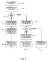
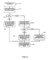
- Figs. 4-6 Although the sequence of Figs. 4-6 indicated that if a fault is detected the data may not be used by the controller, as noted in Fig. 3 at decision step 114, there are certain situations in which a portion of the data can be used. Two examples of which are shown in Figs. 7 and 8.
- an optional initialization error handling routine 200 is shown when an error is detected in which the system controller performs transmission verification on the plus signal path data at 202. If an error is not detected at decision step 204, then the error exists only in the minus signal path data and the system enters a limp mode at step 206, using the plus path data only. At step 208, the system controller uses compensation algorithm data to mathematically correct the plus sense half bridge pressure and temperature data only and at step 210 enters the limp mode of operation in the control algorithm.
- step 212 the system controller performs transmission verification on the minus signal path data. If no error is detected at the decision step 214 then the error exists only in the plus signal path and the system enters the limp mode operating from the minus signal path data only at step 216 and at step 218 the system uses only compensated minus half bridge pressure and temperature data in the control algorithm. If an error is detected at decision step 214 then an error exists in both plus and minus signal paths and a step 220 the system controller reports an error.
- FIG. 8 Another optional error handling routine 250 is shown in Fig. 8 when an error is detected in which the system controller at step 252 performs data verification on the plus signal path compensation data and if no error is detected at decision step 254 then the error exists only in the minus signal path compensation data set and the system enters a limp mode at step 256 operating from the plus signal path only and at step 258 the system controller sets the CS_N pin high, deselecting the sensor MSC ASIC and EEPROM IC as slaves on the SPI bus. If an error is detected at decision step 254 then the system controller at step 260 performs data verification on the minus signal path compensation data set.
- step 262 If no error is detected at decision step 262 then an error exists only in the plus signal path and the system enters the limp mode operating from minus signal path data only and then goes on to step 258 setting the CS_N pin high. If an error is detected at step 262, then an error exists in both the plus and the minus paths of the compensation data sets and at step 266, the system controller reports an error and goes onto step 258 setting the CS_N pin high.
- the transmission of digital data between the sensor ASIC and the system controller avoids deleterious contributions to sensor accuracy in the system. For example, ADC conversion errors in the system, output loading effects on analog signals, and so on.
- the system based computation of the thermally compensated signal provides greater signal accuracy and tighter diagnostic thresholds than can be achieved by a sensor system architecture performing the thermal compensation within the sensor system itself.
- the use of existing computational power of the system controller 14 provides the compensation operation for very little cost, if any, since only a small additional amount of memory for additional program space and data storage is required, and avoids the high cost associated with implementing the thermal compensation in the sensor ASIC, i.e., ASIC die area and test cost.
- the invention provides low cost signal conditioning for multiple sense elements while also providing high accuracy and robust fault coverage by the strategic partitioning of the signal conditioning between the two integrated circuits 10 and 14 to allow low cost per pressure sensing function, improved sensor accuracy and diagnostic capability and by the provision of sense elements each having two half bridges with identical signal conditioning paths for each half.
Landscapes
- Physics & Mathematics (AREA)
- General Physics & Mathematics (AREA)
- Engineering & Computer Science (AREA)
- Technology Law (AREA)
- Measuring Fluid Pressure (AREA)
- Testing Or Calibration Of Command Recording Devices (AREA)
- Measuring Temperature Or Quantity Of Heat (AREA)
Abstract
Description
- This invention relates generally to systems for sensing a variable condition such as pressure, temperature, acceleration, torque, force and the like at a plurality of locations and more particularly to apparatus and methods for signal conditioning multiple sense elements.
- Many applications call for the sensing of a condition, such as pressure, acceleration, torque and force, at a plurality of locations. By way of example in the automotive environment, electro-hydraulic brake or EHB systems generally have six locations that require sensing of the fluid pressure. Pressure sensing is required at each wheel for closed loop brake force control, at a location to sense driver input and at the pressure accumulator to sense system reserve pressure. Hydraulic sensing points are all routed through the hydraulic control unit or HCU having a system controller, i.e., microprocessor, so that there exists one member at which all different hydraulic circuit pressures are sensed. The provision of six discrete pressure sensors with full conditioning electronics results in suitable operation; however, it also results in a total pressure sensor cost which is higher than desirable compared to the remaining system component costs.
- In copending, coassigned application Serial No. 10/036,719 (Attorney Docket No. A41742), the subject matter of which is incorporated herein by this reference, a low cost system and method is disclosed and claimed in which a plurality of bridge type sense elements are connected to an ASIC (application specific integrated circuit) with the output of the sense elements sequentially connected to a common signal conditioning circuit path by analog multiplexing. The sense element signal is conditioned by the signal conditioning circuit of the ASIC to provide partial conditioning comprising basic calibration data. Complete characterization data provided at the time or manufacture for aii the sense elements is stored in non-volatile memory of the ASIC and is transferred to a host controller, e.g., microprocessor, upon command to enable the host controller to perform appropriate mathematical operations to provide the additional amount of compensation required to complete the signal conditioning.
- The ASIC also includes diagnostic fixed test bridges for diagnosing ASIC faults and a signal diagnostic path for diagnosing sense element and sense element connection faults.
- The specific sense elements disclosed in the application are formed of individual strain bridges known in the art, such as silicon resistor bridges bonded to a diaphragm through glass material fired at high temperatures and adapted for placement in a fluid pressure port. When pressurized, fluid in the pressure port causes the diaphragms and bridges to undergo elastic strain. Because the resistors in the bridges are made of silicon, they exhibit a piezoresistive effect exhibiting a change in resistance when subjected to strain. By applying a voltage to the bridges, a small voltage change results at the output of the bridges.
- Although the above system provides diagnostic resolution suitable for certain applications, there is a need for a higher degree of resolution in other applications, particularly in some of the most safety critical applications. For example, the fixed test bridges provide information on specific discrete points of the signal path, in the example shown, two discrete points. While these are effective for a majority of problems, there is a possibility that some errors in the signal path could go undetected.
- Further, with respect to diagnosing sense element and sense element connection faults, the degree of resolution which is possible to obtain is limited due to inherent tolerances of the sensors, signal dependency on the sensed conditions such as pressure and temperature and other behavior associated with strain gauges.
- It is an object of the invention to provide a reliable, low cost sensor having high accuracy as well as the ability to diagnose error problems to a finer resolution than in the prior art system noted above. Another object of the invention is the provision of a low cost sense signal conditioning system for a plurality of sensors responsive to variable conditions such as pressure, force, acceleration, torque, temperature and the like suitable for use with ever more safety critical applications.
- Briefly, in accordance with a preferred embodiment of the invention, a system comprises a multiple sensor ASIC comprising four analog switching multiplexers connected to a plurality of sense elements. Each sense element is made up of two separate half bridges with the bridge bias of each positive bridge half connected to a respective addressable port in one multiplexer and the bridge bias of the minus bridge half connected to a respective addressable port in the second multiplexer. The output of each positive bridge halve is connected to a respective addressable port in the third multiplexer and the output of each minus bridge half is connected to a respective addressable port of the fourth multiplexer.
- The half bridges of each sensor are treated independently of each other having independent variable resistive bridge drives and signal paths. The analog signal paths are mildly trimmable including some offset and gain trim. As in the system described in Serial No. 10/036,719 described above, only the minimum amount of electronic calibration of the pressure and temperature signals are provided in order to minimize complexity and cost as weii as to provide compensation by the system controller with enhanced accuracy and diagnostics. The temperature signal path from the bridge bias voltage is untrimmed since such trimming is unnecessary in the particular example of the preferred embodiment described, but may include trimmable gain for other examples, if desired. The outputs, in the specific embodiment being described, pressure and temperature, in each path are synchronously sampled and the data held and fed into a single analog to digital converter (ADC). The two paths produce opposing pressure and temperature analog signals and due to their opposite polarities, produce a signature which is diagnosed by a system control ASIC. The pressure and temperature information from each path is synchronously sampled, as noted above and fed into a data register which the system control ASIC interfaces over a digital bus, in the present embodiment, a serial peripheral interface or SPI. Although various buses can be employed, the SPI is used due to its low cost and high rate of data throughout required for the particular application.
- The system control ASIC applies a compensation algorithm to generate a fully compensated, highly accurate pressure signal and temperature signal that the system uses as a control variable in the particular application with which the described embodiment is used.
- Information for trimming signals, determined during calibration of the sensor module at the time of manufacture, and coefficients for the compensation algorithm are contained in an electronically erasable programmable read only memory chip (EEPROM) which, in the described embodiment, is external to the multiple sensor ASIC as a cost expedient. Upon power up, the system control ASIC selects the EEPROM through the sensor ASIC by means of the SPI bus and recalls all the coefficients needed to perform selected compensation algorithms and downloads the information. The sensor ASIC trim settings are also recalled from the EEPROM. The exact process is dependent upon the data bus architecture, in the present case an SPI bus; as stated above, the system control ASIC recalls the trim settings from EEPROM and then loads them into the sensor ASIC. The system control ASIC sets up the sensor ASIC by defining the sampling sequence and notifies the system controller when it has completed the sequence. The system controller then recalls the data from the sensor ASIC as needed. The system controller recalls both positive and minus half bridge information, performs compensation algorithms on both halves independently and compares the two signals so that a very precise determination can be made when a sensor is not behaving properly to a finer resolution than is possible using uncompensated half or full bridge data. The system control takes the two compensated pressure and temperature signals, respectively subtracts them to obtain the equivalent of full bridge data.
- The objects, advantages and novel features and methods of the invention will be more fully apparent from the following description when read in connection with the accompany drawings wherein:
- Fig. 1 is a schematic diagram showing a plurality of condition responsive sense elements, each including two separate half bridges, a multiple sensor conditioning circuit in the form of an ASIC, and a non-volatile memory or EEPROM and a system controller in the form of an ASIC;
- Fig. 2 is a schematic block circuit diagram of the multiple sensor ASIC shown in Fig. 1 along with one sense element shown as illustrative;
- Fig. 3 shows an initialization sequence for transfer of compensation data from the pressure sensor to the system controller;
- Figs. 4-6 show a sense element data acquisition sequence; and
- Figs. 7 and 8 show optional initialization error handling routines.
-
- The overall system comprises a pressure sensor system having a plurality of sense elements 1-6, a multiple sensor conditioning (MSC) ASIC 10 and non-volatile memory in the form of
EEPROM chip 12 which interfaces with a host system controller in the form of asystem control ASIC 14. - The MSC ASIC 10 in turn includes multiplexed ASIC inputs capable of interfacing with the sense elements; redundant half bridge conditioning path architecture 10b3, 10b4, to enable system level fault detection of the sense elements and the ASIC; simplified, trimmable signal conditioning paths 10b1, 10b2 with no thermal compensation; and digital transmission of all data by an SPI bus. The sensor system also includes an EEPROM IC 12 external to MSC ASIC 10 for storing
MSC ASIC 10 signal path trim settings (one set for each sense element) and system compensation equation coefficients (one set for each sense element). - A system controller in the form of
system control ASIC 14 is interfaced with the pressure sensor system, using the SPI bus, to read ASIC trim settings and system compensation equation coefficients fromEEPROM 12; using the SPI bus, to write required operating information to MSCASIC 10; and, using the SPI bus, to read pressure, temperature and diagnostic/test data fromMSC ASIC 10. System controller ASIC 14 also performs mathematical compensation of pressure, temperature and diagnostic information in accordance with selected algorithm equations. - With reference to Fig. 1,
numerals 1 and 6 indicate two of a plurality of sense elements, each in the form of a pair of half bridge structures, in the embodiment shown, there are six sense elements but the particular number is a matter of choice. Although in the preferred embodiment the sense elements are responsive to pressure, the sense elements could also be used to sense other variable conditions suitable for such bridge structures such as acceleration, torque and force. - As best seen in Fig. 2, sensor ASIC 10 includes four analog multiplexers, BRM, INM, BRP and INP MUXES, each having six address positions BM1-BM6, IM1-IM6, BP1-BP6 and IP1-IP6. Each sense element half bridge has a bridge node connected to BM1-BM6 respectively for the M half bridges and BP1-BP6 respectively for the P half bridges. Each half bridge has a ground node connected to ground. The output nodes of the M half bridges are respectively connected to address positions IM1-IM6 and the output nodes of the P half bridges are respectively connected to address positions IP1-IP6.
- Half bridge conditioning is provided to enhance sense element fault detection. MSC ASIC 10 includes a first bias and temperature path and a first pressure conditioning path for the positive half bridge and a second bias and temperature path and a second pressure conditioning path for the negative half bridge with the multiplexer address used to determine which sense element at a given time is biased and connected to the half bridge signal conditioning paths.
- For the minus half bridge temperature signal path 10b3, a respective half bridge is selected by multiplexer BRM whose setting is determined by the AM-ADR (address minus-ADR). The half bridge is biased through a programmable series resistor 10a1 whose magnitude is controlled by the RM-REG (resistor minus-REG) value. A low pass filter LPDI is used at the signal input to reject unwanted high frequency signals, for example, EMI or other noise. A fixed amplification is applied to the half bridge bias voltage to increase signal magnitude and improve the resolution of the analog to digital conversion. A sample-and-hold circuit 10c1 stores the signal prior to analog to digital conversion. All the signals to be fed into
ADC 10d are sampled and held at the same time to ensure all data is synchronized in time. - For the minus half bridge pressure signal path 10b1, the corresponding half bridge output is selected by multiplexer INM whose setting is determined by the AM-ADR value. A low pass filter LPFI is used at the signal input to reject unwanted high frequency signals, as in the temperature signal path. The difference between the half bridge output and 1/2 Vbrm (minus half bridge bias voltage reference) is then amplified by a fixed amount. The initial offset voltage of this signal path (e.g., cause by mismatch between the 1/2 Vbrm reference and the half bridge output due to sense element or ASIC tolerance) is cancelled by summing in a portion of the Vbrm into the signal path. The magnitude and sign of the portion of Vbrm to be summed is determined by the BM-REG (bias minus-REG) value. A variable amplification is applied to the half bridge output signal to increase the signal magnitude and improve the resolution of the analog to digital conversion. The magnitude of the applied gain is determined by the GM-REG value. The sample-and-hold circuit 10c2 stores the signal prior to analog to digital conversion. As noted above, all the signals to be fed into
ADC 10d are sampled and held at the same time to ensure all data is synchronized in time. - The analog pressure conditioning paths 10b1, 10b2, contain trimmable offset and gain settings to compensate for sense element variations. Each half bridge has uniquely derived offset and pain trim settings that are stored in specific addresses in Data Register 10e, to be discussed.
- The outputs of the analog temperature and pressure signal conditioning paths are inputted to Sample and Hold circuits 10c1-10c4 and Analog to
Digital Converter ADC 10d. The outputs of the ADC are stored in specific addresses in Data Register 10e. -
Voltage regulator 10g provides bias sources for the analog and ADC circuits. ASIC and sense element test circuits including ADC test and Sample and Hold circuit 10c5 are used during ASIC and sensor production. - Control of
MSC ASIC 10 is achieved by sending specific Data Register contents over the Serial Peripheral Interface (SPI) bus 10h. It should be noted that, if desired, other bus structures could be utilized, however, the SPI is particularly useful in this embodiment due to its low cost and high rate of data throughput. - The SPI bus has a chip select line CS_N, a clock line CLK, a slave input or master output pin SIMO and a slave output or master input pin SOMI. For each connection on the bus there is a chip select line that is unique to each slave with the other lines being common to all the slaves. In the preferred embodiment the
system control ASIC 14 is the master and draws data from and to theMSC ASIC 10 by setting the chip select pin ofsensor MSC ASIC 10 low and then the clock line clocks data into or out ofMSC ASIC 10 which functions as a slave.EEPROM chip 12 is connected to SPI bus 10h. In the specific implementation of the embodiment, when thesystem ASIC 14 calls for information fromEEPROM chip 12 it sets the chip select line ofMSC ASIC 10 low and then sends a command to set the ES_N pin which further selects theEEPROM chip 12 as slave. This particular routine is necessitated by only having one chip select line available fromsystem control ASIC 14 for the pressure sensor system. - As noted above, non-volatile memory in the form of external electrically erasable programmable read only memory (EEPROM)
chip 12 is connected toMSC ASIC 10 to store trim settings and communicates with the system control over the SPI bus, however, there is no direct connection between the system controller and the EPROM chip select soMSC ASIC 10 is used to control the EEPROM chip select. Although the non-volatile memory could be formed as part ofMSC ASIC 10, it is more cost effective to provide the external EEPROM shown. - Typically, the multiple sensor system of the invention is used with a host controller for controlling some function(s) in which the sense information is used. In the present embodiment,
system control ASIC 14 is an automotive brake controller which uses the raw sensor signals to generate fully compensated, highly accurate pressure and temperature signals that the system controller uses as a control variable.System control ASIC 14 has a great deal of computational power and the sensor system made according to the invention takes advantage of this by allocating that portion of the sensor compensation involving complex calculations to provide optimum efficiency while obtaining highly accurate pressure and temperature values used bysystem control ASIC 14 in the brake control. This portion of the sensor compensation will be discussed below in rotation to the compensation algorithms. -
System control ASIC 14 takes the minimally conditionedsensor MSC ASIC 10 digital outputs and applies a mathematical compensation algorithm/equation to achieve the desired values. Although many system compensation algorithms can be employed, the following algorithm is preferred. - Temperature
- TPX is the system compensated temperature signal for positive half bridge, X
- TMPX is the DSM temperature output signal from positive half bridge, X
- TRFP is the temperature offset reference for the positive half bridge calculations
- ATP0X is the zero order compensation coefficient for the selected positive half bridge, X
- ATP1X is the first order compensation coefficient for the selected positive half bridge, X
- ATP2X is the second order compensation coefficient for the selected positive half bridge, X
- ATP3X is the third order compensation coefficient for the selected positive
half bridge, X
- TMX is the system compensated temperature signal for negative half bridge, X
- TMMX is the DSM temperature output signal from negative half bridge, X
- TRFM is a temperature offset reference for the negative half bridge calculations
- ATM0X is the zero order compensation coefficient for the selected negative half bridge, X
- ATM1X is the first order compensation coefficient for the selected negative half bridge, X
- ATM2X is the second order compensation coefficient for the selected negative half bridge, X
- ATM3X is the third order compensation coefficient for the selected negative half bridge, X
- Pressure
- PPX is the system compensated pressure signal from positive half bridge, X
- PRPX is the DSM pressure output signal from positive half bridge, X
- TMPX is the DSM temperature output signal form positive half bridge, X
- TRFP is a temperature offset reference for the positive half bridge calculations
- BP0X is the zero order thermal offset compensation coefficient for the selected positive half bridge, X
- BP1X is the first order thermal offset compensation coefficient for the selected positive half bridge, X
- BP2X is the second order thermal offset compensation coefficient for the selected positive half bridge, X
- GP0X is the zero order thermal gain compensation coefficient for the selected positive half bridge, X
- GP1X is the first order thermal gain compensation coefficient for the selected positive half bridge, X
- GP2X is the second order thermal gain compensation coefficient for the selected positive half bridge, X
- GP3X is the third order thermal gain compensation coefficient for the selected positive half bridge, X
- OP is a compensation equation offset constant
- PMX is the system compensated pressure signal for the selected negative half bridge, X
- PRMX is the DSM pressure output signal for the selected negative half bridge, X
- TMMX is the DSM temperature output signal for the selected negative half bridge, X
- TRFM is a temperature offset reference for the negative half bridge calculations
- BM0X is the zero order thermal offset compensation coefficient for the selected negative half bridge, X
- BM1X is the first order thermal offset compensation coefficient for the selected negative half bridge, X
- BM2X is the second order thermal offset compensation coefficient for the selected negative half bridge, X
- GM0X is the zero order thermal gain compensation coefficient for the selected negative half bridge, X
- GM1X is the first order thermal gain compensation coefficient for the selected negative half bridge, X
- GM2X is the second order thermal gain compensation coefficient for the selected negative half bridge, X
- GM3X is the third order thermal gain compensation coefficient for the selected negative half bridge, X
- OM is compensation equation offset constant
- The system then uses the outputs of the compensation algorithm to derive pressure, temperature and diagnostic information as follows:
- Normal operation (no fault condition exists):
- PX = (PPX - PMX) / 2
- TX = (TPX - TMX)/2
- Limp Mode Operation (a detectable fault condition exists, for example, corruption of positive or negative half bridge EEPROM data):
-
- PX = PPX or PMX
- TX = TPX or TMX
- System Level DSM Diagnostics:
- PDX = (PPX + PMX)/2
- TDX = (TPX + TMX) / 2
- With reference to Fig. 3, the initialization routine loads algorithm compensation coefficients that are stored in
EEPROM 12 to enablesystem ASIC 14 to perform the compensation procedures on the raw data transmitted fromMSC ASIC 10. The initialization routine starts at 100 where power is applied tosystem controller 14 andMSC ASIC 10. Atstep 102, the system controller ASIC sets theMSC ASIC 10 chip select pin, CS_N low selecting the sensor as slave on SPI bus 10h. Atstep 104, the system controller ASIC sends an SPI command to set the ES_N pin low which selectsEEPROM 12 as the slave on the bus. As noted above this particular portion of the routine is employed instead of a conventional implementation ofchip 12 being selected directly byASIC 14 as slave due to a limitation of output pins available in the specific architecture used. Atstep 106,system controller 14 sends an SPI command to read compensation algorithm data from a selectedEEPROM 12 address. EEPROM outputs the data in that address and the routine goes through a loop until the data load is completed as determined bydecision step 108. When the data load is completed thesystem controller 14 sends a command atstep 110 to read the address storing EEPROM verification data. Although various versions can be utilized, the version employed is a cyclical redundancy check (CRC). This is a check,step 112, involving putting the stored data through a mathematical equation that yields a result which is compared atstep 114 to a corresponding result stored inEPROM 12. If an error is detected than the routine loops back to step 106 re-gathering the information. When no error is detected,system controller 14 atstep 116deselects ASIC 10 as slave by setting the CS_N pin to a logic high. - Moving on to Figs. 4-6 which show the sense element (SE) data acquisition sequence,
system controller 14 again sets pin CS_N ofASIC 10 low selecting the sensor as slave on the bus atstep 120. Then atstep 122, the system sends information toASIC 10 which contains the sample sequence configuration for the six sensors and a start bit to initiate sampling. This information includes the order as well as which sensors to be sampled. After this step the routine follows two parallel paths. In one path atstep 124, thecontrol logic 10f decodes the SPI data and configures its own internal circuitry in order to conduct the sampling in the requested order and number. Atstep 126,MSC ASIC 10 sets a "busy" status bit equal to 1, indicating that the sampling sequence is proceeding. Meanwhile in the parallel routine branch atstep 128, the system controller reads the sensor "busy" status bit anddecision step 130 looks to see if the sequence has been completed; if not, the subroutine loops back tostep 128. - Following
step 126 in the first branch, the first sense element in the sampling sequence is selected atstep 132, the circuit data associated with the selected sense element is transferred to the relevant half bridge signal conditioning path atstep 134. Atstep 136, the multiplexers addresses are set selecting the specific bridge whose data is being input to the circuit. A specified time delay is implemented atstep 138 to allow the circuit to stabilize. Following stabilization, the Sample and Hold circuitry simultaneously receive the analog half bridge signal conditioning path outputs atstep 140. The analog todigital converter 10d then atstep 142 sequentially goes through the four signals of the two half bridges as well as an ADC test voltage from Sample and Hold circuit 10c5. - After the analog to digital conversions of the selected sense element pressure, temperature and ADC test voltage are completed, the results are loaded into the data register 10e at
step 144 and followingdecision step 146, if the sequence has not been completed, the routine goes on to the next sense element in the sampling sequence at step 148. If the sequence has been completed followingdecision block 146,MSC ASIC 10 sets the "busy" status bit to zero atstep 150 indicating that the sampling sequence has been completed. - In the meantime, the system controller continues to pole the status of the sequence which is reviewed at
decision block 130, and once the "busy" status bit is changed to zero a command is sent to read data from a selectedMSC ASIC 10 address atstep 152. In the same way that EEPROM 12 was selected in the initialization routine, thesystem controller 14 sends a command which contains a read bit and the address from which the data is to be recalled. The sensor ASIC adds verification information to the data address such as a parity check and transmits the requested data at the address plus the verification information attached to it atstep 154. - The system controller receives the data at
step 156 and performs the appropriate calculations and if the verification calculations match atdecision step 158, then it considers the data as valid. If they do not match an error is indicated and the routine loops back to step 152 to reread the data. If no error is detected, the sense element half bridge data and ADC test results are transferred to system memory atstep 160 and the data load cycle continues until all the information for all the requested sense elements has been completed as determined indecision step 162. - When the data load is completed, the system controller at
step 164 uses the compensation algorithm data it recalled during the initialization sequence and applies it to the sense element half bridge pressure and temperature data using the above described compensation algorithms. Atstep 166, the system controller compares the positive and minus sense element half bridge compensation algorithm outputs and atdecision step 168 if a fault is detected the system does not use the data but reports an error atstep 170. If no error is detected, the system controller then compares the ADC test results with predefined fault bands atstep 172 and if a fault is detected atdecision step 174, again the data is not used by the system controller and an error reported atstep 170. If no error is detected then the data is considered valid and the system controller uses the compensated sense element pressure and temperature data in its control algorithm (not shown). - Although the sequence of Figs. 4-6 indicated that if a fault is detected the data may not be used by the controller, as noted in Fig. 3 at
decision step 114, there are certain situations in which a portion of the data can be used. Two examples of which are shown in Figs. 7 and 8. - With reference to Fig. 7, an optional initialization error handling routine 200 is shown when an error is detected in which the system controller performs transmission verification on the plus signal path data at 202. If an error is not detected at
decision step 204, then the error exists only in the minus signal path data and the system enters a limp mode atstep 206, using the plus path data only. Atstep 208, the system controller uses compensation algorithm data to mathematically correct the plus sense half bridge pressure and temperature data only and atstep 210 enters the limp mode of operation in the control algorithm. - Going back to
decision step 204, if an error is detected in the plus signal path then atstep 212 the system controller performs transmission verification on the minus signal path data. If no error is detected at thedecision step 214 then the error exists only in the plus signal path and the system enters the limp mode operating from the minus signal path data only atstep 216 and atstep 218 the system uses only compensated minus half bridge pressure and temperature data in the control algorithm. If an error is detected atdecision step 214 then an error exists in both plus and minus signal paths and astep 220 the system controller reports an error. - Another optional error handling routine 250 is shown in Fig. 8 when an error is detected in which the system controller at
step 252 performs data verification on the plus signal path compensation data and if no error is detected atdecision step 254 then the error exists only in the minus signal path compensation data set and the system enters a limp mode at step 256 operating from the plus signal path only and atstep 258 the system controller sets the CS_N pin high, deselecting the sensor MSC ASIC and EEPROM IC as slaves on the SPI bus. If an error is detected atdecision step 254 then the system controller atstep 260 performs data verification on the minus signal path compensation data set. If no error is detected atdecision step 262 then an error exists only in the plus signal path and the system enters the limp mode operating from minus signal path data only and then goes on to step 258 setting the CS_N pin high. If an error is detected atstep 262, then an error exists in both the plus and the minus paths of the compensation data sets and atstep 266, the system controller reports an error and goes ontostep 258 setting the CS_N pin high. - In accordance with the invention, the transmission of digital data between the sensor ASIC and the system controller avoids deleterious contributions to sensor accuracy in the system. For example, ADC conversion errors in the system, output loading effects on analog signals, and so on. The system based computation of the thermally compensated signal provides greater signal accuracy and tighter diagnostic thresholds than can be achieved by a sensor system architecture performing the thermal compensation within the sensor system itself. Further, the use of existing computational power of the
system controller 14 provides the compensation operation for very little cost, if any, since only a small additional amount of memory for additional program space and data storage is required, and avoids the high cost associated with implementing the thermal compensation in the sensor ASIC, i.e., ASIC die area and test cost. The invention provides low cost signal conditioning for multiple sense elements while also providing high accuracy and robust fault coverage by the strategic partitioning of the signal conditioning between the twointegrated circuits - While a preferred embodiment of the present invention has been disclosed in detail, it should be understood that various modifications, such as using sense elements responsive to conditions other than pressure, such as acceleration, torque, force and the like mentioned supra, may be adopted without departing from the spirit of the invention or scope of the appended claims. Further, although non-volatile memory is used in the preferred embodiment, it is within the purview of the invention to use other forms of data storage, such as bar code labels or the like.
Claims (17)
- A variable condition responsive sensor system comprising at least one variable condition sense element having first and second outputs, the variable condition being one of pressure, acceleration, force and torque,
first and second signal conditioning paths, the first output of the at least one sense element connected to the first signal conditioning path and the second output of the at least one sense element connected to the second signal conditioning path,
memory for storing calibration and characterization data for the at least one sense element and the signal conditioning paths, and
an interface circuit for transmitting data from the memory to the signal conditioning components for separately conditioning the signals of the at least one sense element and to an external controller to perform mathematical corrections of the conditioned signals and for comparing the conditioned signals of the at least one sense element. - A variable condition responsive sensor according to claim 1 in which the at least one variable condition sense element comprises first and second half bridges, the first half bridge providing the first output and the second half bridge providing the second output.
- A variable condition responsive sensor system according to claim 2 in which there are a plurality of sense elements and further comprising at least one multiplexer with addressable ports connected to the outputs of each half bridge of the plurality of sense elements, the at least one multiplexer having output ports, an output port connected to each signal conditioning path.
- A variable condition responsive sensor system according to claim 2 in which each half bridge has a bias node and a ground node and further comprising an independent variable resistor connected in series between a voltage source and an output port of the at least one multiplexer.
- A variable condition responsive sensor system according to claim 3 in which the signal conditioning paths and the at least one multiplexer are formed in an ASIC.
- A variable condition responsive sensor system according to claim 5 in which the memory is non-volatile.
- A variable condition responsive sensor system according to claim 6 in which the non-volatile memory is formed in a separate IC.
- A variable condition responsive sensor system according to claim 1 in which the variable condition is pressure.
- A variable condition responsive sense element system comprising
a plurality of variable condition responsive sense elements providing an output dependent on the variable condition, the variable condition being one of pressure, acceleration, force and torque, the sense elements each having first and second half bridges, each bridge half having a bias node, a ground node and a respective positive and minus output node,
a voltage source,
an electronic circuit having first, second, third and fourth multiplexers, each having an output and a plurality of address input positions,
a respective independent variable resistor connected in series between the voltage source and the output of each of the first and third multiplexers, the bias node of each half bridge of each sense element connected to a respective multiplexer address position of the respective first and third multiplexers,
separate signal conditioning paths,
the minus output node of each sense element connected to a respective multiplexer address position of the second multiplexer, the positive node of each sense element connected to a respective multiplexer address position of the fourth multiplexer,
a respective separate signal path connected to the output of each multiplexer,
an analog to digital converter having a plurality of inputs and an output, the signal paths being connected to the inputs of the analog to digital converter,
a data register having an input and an output, the output of the analog to digital converter connected to the input of the data register,
a data transfer circuit connected to the data register and having connections for an external controller, said data transfer circuit capable of transferring data to and from the external controller, and
a memory, the memory being connected to the data transfer circuit, the memory providing analog trim settings for the sense element signal paths, and data for the external controller enabling the external controller to perform mathematical compensation for the variable condition sense element signals. - A variable condition responsive sensor system according to claim 9 in which the data transfer circuit is a serial peripheral interface bus.
- A method performed with a variable condition responsive sensor system having a plurality of variable condition sense elements, the method comprising:forming each of the sense bridge elements into two portions, each portion having an output node,separately conditioning output signals from each output node of a selected sense element,comparing the separately conditioned signals of the portions of the selected sense element with each other to determine whether the conditioned signals come within selected tolerance bands.
- The method claim 11 in which the variable condition sense elements each comprise a bridge having two halves, each half having one of the output nodes.
- The method of claim 12 in which the step of comparing the separately conditioned signals includes subtracting the conditioned signal of one half bridge from the conditional signal of the other half bridge of a sense element and taking the average of the difference in the two conditioned signals.
- The method of claim 12 further comprising
forming an electronic circuit having signal conditioning paths, the paths having signal conditioning components for each half bridge output,
obtaining electronic calibration data for each sense element during manufacture of the sensor system and storing that information in memory,
connecting the outputs of the bridge halves of a selected sense element to the respective signal conditioning circuit paths using basic calibration data from the memory and separately, partially conditioning the selected output signal, and
completing the separate conditioning of the partially conditioned signal by performing mathematical corrections using data transferred from the non-volatile memory to obtain fully conditioned signals before the comparison step of the separately conditioned signals. - The method of claim 12 further comprising
forming an electronic circuit having multiplexers, a signal conditioning path having signal conditioning components for each half bridge output, an analog to digital converter, memory and an interface circuit for transmitting and receiving data,
obtaining electronic calibration data for each half bridge sense element during manufacture of the sensor system and storing that information in memory,
connecting the electronic circuit to an external controller,
transmitting data from memory to enable the external controller to perform mathematical corrections to a conditional digital signal,
selecting an address of the multiplexers for connecting the output of a selected half bridge of a selected sense element to the respective signal conditioning circuit path and to transmit basic calibration data to the signal conditioning components in the signal conditioning path,
partially conditioning the addressed sense element half bridge using the basic calibration data transmitted from memory to provide a partially conditioned signal,
converting the partially conditioned signal from an analog format to a digital format in the analog to digital converter to provide a digital signal,
transmitting the digital signal to the external controller,
completing the conditioning of the partially conditioned signal by performing mathematical corrections to the digital signal in the external controller using the data transferred from the memory to obtain fully separately conditioned signals before the comparison step of the separately conditioned signals. - The method of claim 15 in which the interface circuit comprises a serial peripheral interface bus.
- The method of claim 15 in which each half bridge has a bias node and further comprising the step of multiplexing the bias node into connection with an independent variable resistor serially connected to a voltage source.
Applications Claiming Priority (2)
| Application Number | Priority Date | Filing Date | Title |
|---|---|---|---|
| US10/743,363 US7031863B2 (en) | 2003-12-22 | 2003-12-22 | Variable condition responsive sense system and method |
| US743363 | 2003-12-22 |
Publications (2)
| Publication Number | Publication Date |
|---|---|
| EP1548417A1 true EP1548417A1 (en) | 2005-06-29 |
| EP1548417B1 EP1548417B1 (en) | 2012-05-09 |
Family
ID=34552827
Family Applications (1)
| Application Number | Title | Priority Date | Filing Date |
|---|---|---|---|
| EP04257249A Expired - Lifetime EP1548417B1 (en) | 2003-12-22 | 2004-11-23 | Sensor system for measuring variable physical quantities |
Country Status (3)
| Country | Link |
|---|---|
| US (1) | US7031863B2 (en) |
| EP (1) | EP1548417B1 (en) |
| JP (1) | JP4549176B2 (en) |
Cited By (3)
| Publication number | Priority date | Publication date | Assignee | Title |
|---|---|---|---|---|
| WO2013160073A1 (en) * | 2012-04-27 | 2013-10-31 | Robert Bosch Gmbh | Sensor time synchronization |
| WO2016113653A1 (en) * | 2015-01-12 | 2016-07-21 | Murata Manufacturing Co., Ltd. | Continuous self-test in capacitive sensor |
| US12013259B2 (en) | 2018-09-26 | 2024-06-18 | Infineon Technologies Ag | Providing compensation parameters for sensor integrated circuits |
Families Citing this family (11)
| Publication number | Priority date | Publication date | Assignee | Title |
|---|---|---|---|---|
| US7007552B2 (en) * | 2004-07-26 | 2006-03-07 | Texas Instruments Incorporated | Multi-channel pressure sensing apparatus |
| US7451053B2 (en) * | 2005-09-29 | 2008-11-11 | Hynix Semiconductor Inc. | On die thermal sensor of semiconductor memory device and method thereof |
| DE102005047971B4 (en) * | 2005-10-06 | 2008-01-17 | Dr.-Ing. Gschwind Elektronik Gmbh | Load measuring device |
| US20110301414A1 (en) * | 2010-06-04 | 2011-12-08 | Robert Hotto | Intelligent endoscopy systems and methods |
| CN102455237A (en) * | 2010-11-01 | 2012-05-16 | 南车洛阳机车有限公司 | Digital display pressure gauge test bed |
| US8461879B1 (en) * | 2012-05-28 | 2013-06-11 | Active-Semi, Inc. | Low latency inter-die trigger serial interface for ADC |
| US9348383B2 (en) * | 2013-03-01 | 2016-05-24 | Intel Corporation | Apparatus for starting up switching voltage regulator |
| DE102013206646A1 (en) * | 2013-04-15 | 2014-10-16 | Siemens Aktiengesellschaft | Transducer for process instrumentation and method for its diagnosis |
| CN209326840U (en) | 2018-12-27 | 2019-08-30 | 热敏碟公司 | Pressure sensor and pressure transmitter |
| EP3949845B1 (en) | 2019-03-27 | 2024-02-14 | Nitto Denko Corporation | Data acquisition apparatus and biological sensor |
| CN112563145A (en) * | 2020-11-26 | 2021-03-26 | 娄底市安地亚斯电子陶瓷有限公司 | Preparation method of ceramic circuit of automobile preparation pressure strain gauge |
Citations (3)
| Publication number | Priority date | Publication date | Assignee | Title |
|---|---|---|---|---|
| US4574356A (en) | 1982-02-11 | 1986-03-04 | Minister Of National Defence Of Her Majesty's Canadian Government | Peak dynamic stress calculator |
| EP1111344A1 (en) | 1999-12-20 | 2001-06-27 | Texas Instruments Incorporated | Sensor fault detection method and apparatus |
| EP1235053A2 (en) | 2001-01-26 | 2002-08-28 | Texas Instruments Incorporated | Apparatus and method for collecting and processing data from a plurality of sensors |
Family Cites Families (7)
| Publication number | Priority date | Publication date | Assignee | Title |
|---|---|---|---|---|
| USH81H (en) * | 1984-09-24 | 1986-07-01 | The United States Of America As Represented By The Secretary Of The Army | Projectile guidance recording system |
| US5014238A (en) * | 1987-07-15 | 1991-05-07 | Distributed Matrix Controls Inc. | Universal input/output device |
| US5068811A (en) * | 1990-07-27 | 1991-11-26 | Bha Group, Inc. | Electrical control system for electrostatic precipitator |
| DE19728381B4 (en) * | 1997-07-03 | 2006-11-09 | Robert Bosch Gmbh | Method and circuit for monitoring the function of a sensor bridge |
| US6422088B1 (en) * | 1999-09-24 | 2002-07-23 | Denso Corporation | Sensor failure or abnormality detecting system incorporated in a physical or dynamic quantity detecting apparatus |
| JP2002298279A (en) * | 2001-01-26 | 2002-10-11 | Texas Instruments Inc | State response detection system and method |
| US6765391B2 (en) * | 2002-10-22 | 2004-07-20 | Texas Instruments Incorporated | Low cost asic architecture for safety critical applications monitoring an applied stimulus |
-
2003
- 2003-12-22 US US10/743,363 patent/US7031863B2/en not_active Expired - Lifetime
-
2004
- 2004-11-23 EP EP04257249A patent/EP1548417B1/en not_active Expired - Lifetime
- 2004-12-21 JP JP2004369469A patent/JP4549176B2/en not_active Expired - Fee Related
Patent Citations (3)
| Publication number | Priority date | Publication date | Assignee | Title |
|---|---|---|---|---|
| US4574356A (en) | 1982-02-11 | 1986-03-04 | Minister Of National Defence Of Her Majesty's Canadian Government | Peak dynamic stress calculator |
| EP1111344A1 (en) | 1999-12-20 | 2001-06-27 | Texas Instruments Incorporated | Sensor fault detection method and apparatus |
| EP1235053A2 (en) | 2001-01-26 | 2002-08-28 | Texas Instruments Incorporated | Apparatus and method for collecting and processing data from a plurality of sensors |
Cited By (5)
| Publication number | Priority date | Publication date | Assignee | Title |
|---|---|---|---|---|
| WO2013160073A1 (en) * | 2012-04-27 | 2013-10-31 | Robert Bosch Gmbh | Sensor time synchronization |
| US9383234B2 (en) | 2012-04-27 | 2016-07-05 | Robert Bosch Gmbh | Sensor time synchronization |
| WO2016113653A1 (en) * | 2015-01-12 | 2016-07-21 | Murata Manufacturing Co., Ltd. | Continuous self-test in capacitive sensor |
| US10024882B2 (en) | 2015-01-12 | 2018-07-17 | Murata Manufacturing Co., Ltd. | Continuous self-test in capacitive sensor |
| US12013259B2 (en) | 2018-09-26 | 2024-06-18 | Infineon Technologies Ag | Providing compensation parameters for sensor integrated circuits |
Also Published As
| Publication number | Publication date |
|---|---|
| JP4549176B2 (en) | 2010-09-22 |
| US20050137821A1 (en) | 2005-06-23 |
| JP2005181337A (en) | 2005-07-07 |
| EP1548417B1 (en) | 2012-05-09 |
| US7031863B2 (en) | 2006-04-18 |
Similar Documents
| Publication | Publication Date | Title |
|---|---|---|
| EP1235053B1 (en) | Apparatus and method for collecting and processing data from a plurality of sensors | |
| US7031863B2 (en) | Variable condition responsive sense system and method | |
| EP0980601B1 (en) | Signal conditioning circuit including a combined adc/dac, sensor system, and method therefor | |
| JP5173115B2 (en) | Field transmitter with diagnostic self-test mode | |
| EP0909378B1 (en) | A system and method for high accuracy calibration of a sensor for offset and sensitivity variation with temperature | |
| EP1111344B1 (en) | Sensor fault detection method and apparatus | |
| CN102187571B (en) | The self-automatic calibration of the analog circuit in composite signal integrated circuits device | |
| US20020078732A1 (en) | Method and apparatus for the calibration and compensation of sensors | |
| WO1989004089A1 (en) | Transmitter with internal serial bus | |
| US20050190088A1 (en) | Electronic circuit arrangement for error-free analog/digital conversion of signals | |
| US6765391B2 (en) | Low cost asic architecture for safety critical applications monitoring an applied stimulus | |
| JP4936337B2 (en) | Status response detection system and method | |
| EP0972243B1 (en) | Polynomial calculator device | |
| US8326581B2 (en) | Crash sensor and method for processing at least one measuring signal | |
| EP4707761A1 (en) | Pressure sensor, method, brake system, vehicle and use of a pressure sensor | |
| US5798692A (en) | Digital compensation circuit for calibration of sensors | |
| JP2009096338A (en) | Control system | |
| US12618881B2 (en) | Device and method for ratiometric measurement of voltages for an analog-digital-converter | |
| EP4056954B1 (en) | Active measurement correction of resistive sensors | |
| US20240133929A1 (en) | Device and method for ratiometric measurement of voltages for an analog-digital-converter | |
| JPH02206730A (en) | Self-diagnostic circuit | |
| CN120403952A (en) | A collective pitch rod force detection system and method |
Legal Events
| Date | Code | Title | Description |
|---|---|---|---|
| PUAI | Public reference made under article 153(3) epc to a published international application that has entered the european phase |
Free format text: ORIGINAL CODE: 0009012 |
|
| AK | Designated contracting states |
Kind code of ref document: A1 Designated state(s): AT BE BG CH CY CZ DE DK EE ES FI FR GB GR HU IE IS IT LI LU MC NL PL PT RO SE SI SK TR |
|
| AX | Request for extension of the european patent |
Extension state: AL HR LT LV MK YU |
|
| 17P | Request for examination filed |
Effective date: 20050823 |
|
| AKX | Designation fees paid |
Designated state(s): DE FR GB |
|
| RAP1 | Party data changed (applicant data changed or rights of an application transferred) |
Owner name: SENSATA TECHNOLOGIES, INC. |
|
| GRAP | Despatch of communication of intention to grant a patent |
Free format text: ORIGINAL CODE: EPIDOSNIGR1 |
|
| RTI1 | Title (correction) |
Free format text: SENSOR SYSTEM FOR MEASURING VARIABLE PHYSICAL QUANTITIES |
|
| GRAS | Grant fee paid |
Free format text: ORIGINAL CODE: EPIDOSNIGR3 |
|
| GRAA | (expected) grant |
Free format text: ORIGINAL CODE: 0009210 |
|
| AK | Designated contracting states |
Kind code of ref document: B1 Designated state(s): DE FR GB |
|
| REG | Reference to a national code |
Ref country code: GB Ref legal event code: FG4D |
|
| REG | Reference to a national code |
Ref country code: DE Ref legal event code: R096 Ref document number: 602004037726 Country of ref document: DE Effective date: 20120705 |
|
| PGFP | Annual fee paid to national office [announced via postgrant information from national office to epo] |
Ref country code: FR Payment date: 20121010 Year of fee payment: 9 |
|
| PLBE | No opposition filed within time limit |
Free format text: ORIGINAL CODE: 0009261 |
|
| STAA | Information on the status of an ep patent application or granted ep patent |
Free format text: STATUS: NO OPPOSITION FILED WITHIN TIME LIMIT |
|
| 26N | No opposition filed |
Effective date: 20130212 |
|
| REG | Reference to a national code |
Ref country code: DE Ref legal event code: R097 Ref document number: 602004037726 Country of ref document: DE Effective date: 20130212 |
|
| REG | Reference to a national code |
Ref country code: FR Ref legal event code: ST Effective date: 20140731 |
|
| PG25 | Lapsed in a contracting state [announced via postgrant information from national office to epo] |
Ref country code: FR Free format text: LAPSE BECAUSE OF NON-PAYMENT OF DUE FEES Effective date: 20131202 |
|
| PGFP | Annual fee paid to national office [announced via postgrant information from national office to epo] |
Ref country code: DE Payment date: 20161130 Year of fee payment: 13 Ref country code: GB Payment date: 20161026 Year of fee payment: 13 |
|
| REG | Reference to a national code |
Ref country code: DE Ref legal event code: R119 Ref document number: 602004037726 Country of ref document: DE |
|
| GBPC | Gb: european patent ceased through non-payment of renewal fee |
Effective date: 20171123 |
|
| PG25 | Lapsed in a contracting state [announced via postgrant information from national office to epo] |
Ref country code: DE Free format text: LAPSE BECAUSE OF NON-PAYMENT OF DUE FEES Effective date: 20180602 |
|
| PG25 | Lapsed in a contracting state [announced via postgrant information from national office to epo] |
Ref country code: GB Free format text: LAPSE BECAUSE OF NON-PAYMENT OF DUE FEES Effective date: 20171123 |