EP1548275A1 - Control circuit for an electronic driving device of inductive loads, in particular for a device with an input signal having, at the high logic state, non optimal voltage value - Google Patents
Control circuit for an electronic driving device of inductive loads, in particular for a device with an input signal having, at the high logic state, non optimal voltage value Download PDFInfo
- Publication number
- EP1548275A1 EP1548275A1 EP03425763A EP03425763A EP1548275A1 EP 1548275 A1 EP1548275 A1 EP 1548275A1 EP 03425763 A EP03425763 A EP 03425763A EP 03425763 A EP03425763 A EP 03425763A EP 1548275 A1 EP1548275 A1 EP 1548275A1
- Authority
- EP
- European Patent Office
- Prior art keywords
- current
- circuit according
- voltage
- power element
- control
- Prior art date
- Legal status (The legal status is an assumption and is not a legal conclusion. Google has not performed a legal analysis and makes no representation as to the accuracy of the status listed.)
- Granted
Links
- 230000001939 inductive effect Effects 0.000 title claims abstract description 19
- 238000005516 engineering process Methods 0.000 claims description 5
- 239000004065 semiconductor Substances 0.000 description 4
- 238000004088 simulation Methods 0.000 description 4
- 238000004804 winding Methods 0.000 description 4
- 238000011156 evaluation Methods 0.000 description 3
- 238000002485 combustion reaction Methods 0.000 description 1
- 238000010586 diagram Methods 0.000 description 1
- 238000004880 explosion Methods 0.000 description 1
- 238000000605 extraction Methods 0.000 description 1
- 239000000203 mixture Substances 0.000 description 1
- 239000000758 substrate Substances 0.000 description 1
- 239000011800 void material Substances 0.000 description 1
Images


Classifications
-
- F—MECHANICAL ENGINEERING; LIGHTING; HEATING; WEAPONS; BLASTING
- F02—COMBUSTION ENGINES; HOT-GAS OR COMBUSTION-PRODUCT ENGINE PLANTS
- F02P—IGNITION, OTHER THAN COMPRESSION IGNITION, FOR INTERNAL-COMBUSTION ENGINES; TESTING OF IGNITION TIMING IN COMPRESSION-IGNITION ENGINES
- F02P3/00—Other installations
- F02P3/02—Other installations having inductive energy storage, e.g. arrangements of induction coils
- F02P3/04—Layout of circuits
- F02P3/0407—Opening or closing the primary coil circuit with electronic switching means
- F02P3/0435—Opening or closing the primary coil circuit with electronic switching means with semiconductor devices
-
- H—ELECTRICITY
- H03—ELECTRONIC CIRCUITRY
- H03K—PULSE TECHNIQUE
- H03K17/00—Electronic switching or gating, i.e. not by contact-making and –breaking
- H03K17/04—Modifications for accelerating switching
- H03K17/0406—Modifications for accelerating switching in composite switches
-
- H—ELECTRICITY
- H03—ELECTRONIC CIRCUITRY
- H03K—PULSE TECHNIQUE
- H03K17/00—Electronic switching or gating, i.e. not by contact-making and –breaking
- H03K17/04—Modifications for accelerating switching
- H03K17/042—Modifications for accelerating switching by feedback from the output circuit to the control circuit
- H03K17/04206—Modifications for accelerating switching by feedback from the output circuit to the control circuit in field-effect transistor switches
-
- H—ELECTRICITY
- H03—ELECTRONIC CIRCUITRY
- H03K—PULSE TECHNIQUE
- H03K17/00—Electronic switching or gating, i.e. not by contact-making and –breaking
- H03K17/08—Modifications for protecting switching circuit against overcurrent or overvoltage
- H03K17/082—Modifications for protecting switching circuit against overcurrent or overvoltage by feedback from the output to the control circuit
- H03K17/0828—Modifications for protecting switching circuit against overcurrent or overvoltage by feedback from the output to the control circuit in composite switches
-
- F—MECHANICAL ENGINEERING; LIGHTING; HEATING; WEAPONS; BLASTING
- F02—COMBUSTION ENGINES; HOT-GAS OR COMBUSTION-PRODUCT ENGINE PLANTS
- F02D—CONTROLLING COMBUSTION ENGINES
- F02D41/00—Electrical control of supply of combustible mixture or its constituents
- F02D41/20—Output circuits, e.g. for controlling currents in command coils
- F02D2041/2017—Output circuits, e.g. for controlling currents in command coils using means for creating a boost current or using reference switching
-
- F—MECHANICAL ENGINEERING; LIGHTING; HEATING; WEAPONS; BLASTING
- F02—COMBUSTION ENGINES; HOT-GAS OR COMBUSTION-PRODUCT ENGINE PLANTS
- F02D—CONTROLLING COMBUSTION ENGINES
- F02D41/00—Electrical control of supply of combustible mixture or its constituents
- F02D41/20—Output circuits, e.g. for controlling currents in command coils
- F02D2041/2068—Output circuits, e.g. for controlling currents in command coils characterised by the circuit design or special circuit elements
- F02D2041/2075—Type of transistors or particular use thereof
Definitions
- the present invention relates to a control circuit for an electronic driving device of inductive loads.
- the invention relates to a control circuit for an electronic driving device of inductive loads, of the type comprising at least a control block activated by a trigger signal and output-connected to a control terminal of a power element connected in turn to an inductive load.
- the invention relates to a control circuit for an electronic driving device of inductive loads, in electronic ignition applications and smart power devices, and the following description is made with reference to this field of application for convenience of illustration only.
- a linear control circuit is generally capable of driving a power element, also allowing the highest voltage and deliverable current to be protected and diagnostic functions to be performed.
- figure 1a shows a known solution, a control block 1 driving a first power element, in particular an IGBT transistor TR1 of an electronic device 2.
- the block 1 is powered by a supply voltage Vbat and activated by a trigger signal V TRIGGER .
- the first power element TR1 is inserted between a first voltage reference, in particular a supply voltage Vbat and a second voltage reference, for example a ground GND and it has a first conduction terminal, in particular a collector terminal C, connected to the first voltage reference Vbat, a second conduction terminal, in particular an emitter terminal E, connected to the ground GND, as well as a control terminal, in particular a gate terminal G connected to the control block
- a second power element in particular an IGBT sensing transistor TR1 SENSE , and a sensing resistance Rs are connected in series to each other and in parallel between the terminals C and E of the first power element.
- the two power elements TR1 and TR1 SENSE are crossed by different fractions of a same conduction current I COIL .
- Figure 1b shows a second known solution wherein the components and signals being already present in figure 1a will keep the same label; figure 1b shows a control block 10, changed with respect to block 1.
- the supply voltage of block 10 coincides with the voltage at the high state of the trigger signal, being used in the meantime to activate the block.
- the object of the present invention relates to the family of the products shown in figure 1b which, not using an external power supply, can be assembled in simpler and cheaper packages like three-pin-packages.
- the electronic device 2 correctly operates even in the worst case occurring for low battery voltages Vbat and at extreme temperatures, when the trigger voltage V TRIGGER , at the high state, can be reduced; for example, being the signal ground separated from the power ground, the real voltage being applied between the gate G and emitter E terminals of said first power element TR1 is further reduced by the voltage fall ⁇ V introduced by connection cables and connectors.
- FIG 2 shows the same control block 10 of figure 1b, wherein the voltage fall introduced by cables and connectors is also underlined; the components and signals being already present in figure 1b will keep the same label also in figure 2.
- a power element in the case of figure 2 the first power element TR1, is capable of delivering an output current I COIL no lower than 17A, with a trigger signal V TRIGGER at the input of the block whose intensity is equal to 5V.
- the highest voltage being applicable on the gate terminal G is given by the trigger voltage V TRIGGER minus the voltage fall ⁇ V introduced by the control block 10.
- the highest output current I COIL deliverable by the device is also set.
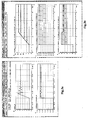
- Figures 3a and 3b shows in a series of graphs signals related to simulations on the block of figure 2 performed for the first power element TR1, in particular an IGBT transistor whose active area is equal to 10 mm 2 , driven by the control block 10 limiting the output current I COIL to 20A.
- Figure 3a relates to the case of the trigger voltage V TRIGGER at the high state of 2.5V and figure 3b quotes the simulation results as the amplitude of said voltage varies.
- the output current I(COIL_1) keeps lower than 4 A, i.e. quite lower than the predetermined limitation current, since the voltage V(GATE_1) calculated on the gate terminal G corresponds to about 2.3V.
- the IGBT transistor TR1 When the trigger signal V TRIGGER reaches a low state, the IGBT transistor TR1 is disabled and the power accumulated in the primary winding 3A of a coil transfers to the secondary winding generating a spark on the igniter plug 3B.
- the prior art suggests the use of a charge pump fed by a trigger signal V TRIGGER , capable of generating an output voltage being sufficiently high as to conveniently bias the gate terminal G of said IGBT transistor TR1, allowing thus the current ICOIL required by the application to be delivered therefrom.
- this solution has a serious drawback: the noise generated by the inner oscillator of the charge pump can cause electromagnetic noises making the device incompatible with the regulations.
- the technical problem underlying the present invention is to provide a control circuit of electronic devices, having such structural and functional features as to ensure also in the worst case, i.e. with a reduced amplitude of the trigger signal, a sufficiently high current as to avoid ignition problems, overcoming the limits and/or drawbacks still affecting the devices realised according to the prior art.
- the solution idea underlying the present invention is to insert an auxiliary current generator capable of delivering an auxiliary current to be added to the current outputted by the control circuit in order to bias, according to the provided specifications, the control terminal of the controlled device power element.
- Figure 5 shows a control circuit 6 receiving at its input a trigger signal V TRIGGER and a collector voltage value V L and outputting a current value I GATE driving a first power element, particularly an IGBT transistor TR1 of a driving circuit 9 of inductive loads.
- control circuit 6 comprises a control block 10 receiving, as in the prior art, at its input said trigger signal V TRIGGER and generating a first current I DRIV .
- the control circuit 6 also comprises, according to the invention, a current generator block A receiving at its input said collector voltage V L and producing a second current, in particular an auxiliary current I AUX .
- said input voltage V L of the control circuit 6, by means of the auxiliary current I AUX generator block A, is detected in a point L coinciding with a terminal, in particular the cathode terminal which is common to two intrinsic diodes D1 and D2 located in series between the collector and the emitter of said power element TR1 of said electronic driving device 9 of inductive loads.
- Said voltage V L is proportional to the collector voltage of said power element TR1 and it is drawn in an area located between the substrate n and p of the physical structure of the transistor itself.
- the contributions of said currents - first I DRIV and second I AUX - are added, by means of a logic gate OR, and they output said current I GATE to control said power element TR1 of said electronic driving device 9 of inductive loads.
- Said power element TR1 is associated, as already described in the prior art, to a second power element, in particular an IGBT sensing transistor TR SENSE .
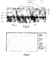
- Figure 4 shows the structure used to draw said voltage V L from said IGBT transistor TR1 of said electronic driving device 9 of inductive loads, used to feed said auxiliary current I AUX generator block A.
- This figure 4 schematically shows an integrated structure comprising the first power element TR1.
- a bonding pad is provided near the edge structure of said power element TR1 in order to draw the value of the collector voltage V L .
- the composed structure of the transistor TR1 comprises, on the collector layer 11, a first semiconductor layer 12 of a first conductivity type P, heavily doped (P+), topped by a second semiconductor layer 13 of a second conductivity type (N), heavily doped (N+).
- the additional pad 19 is located on the edge of the transistor TR1 structure; by means of said pad 19, the collector voltage V L of said transistor is drawn, and it is brought back to the input of said auxiliary current I AUX generator block A.
- Figure 4 also shows, overlapped, the circuit equivalent of said connection 10 represented by the series of two diodes with common cathode.
- This solution has the advantage of pinching at high voltage, as shown in the curve of figure 6.
- a second possible optional solution to realise the auxiliary current I AUX generator block A is the use of a third power element, in particular a JFET transistor TR2 which can be integrated inside the same IGBT transistor TR1 of said electronic driving device 9 of inductive loads; advantageusly, according to the invention, in this case, said control circuit 6 can be realised with a low voltage technology.
- figure 7 describes a circuit realised to evaluate the effectiveness of this second solution.
- the JFET transistor TR2 has the control terminal coinciding with the emitter E of said transistor TR1, a first conduction terminal connected to said cathode terminal L being common to said two intrinsic diodes D1 and D2 and a second conduction terminal coupled to the gate terminal G of the transistor TR1 of said driving circuit 8 of inductive loads.
- a diode D3 is inserted between said second conduction terminal of the JFET transistor TR2 and the gate terminal G of the transistor TR1, while a Zener diode Dz is connected between the second conduction terminal of the JFET transistor TR2 and the ground GND.
- An operational amplifier OP1 is also provided, serving as current limiter, with an inverting input (-) connected to a generator block 8 of reference voltage VREF, receiving at its input said trigger signal V TRIGGER , a non inverting input (+) connected to the emitter terminal E SENSE of said sensing transistor TR1 SENSE and an output connected to the gate terminal G of the transistor TR1.
- the voltage reference block 8 and the operational amplifier OP1 serving as current limiter allow the limitation function of the highest current outputted from said first transistor TR1 to be performed.
- control block 10 has the following features:
- Figures 8a and 8b quote the result of the simulation of the circuit of figure 7.
- the control terminal G capacity is charged in two following steps:
- the voltage on said control terminal G of said transistor TR1 is at the end limited by the operational amplifier OP1 serving as current limiter, operating in adjustment, in order to have the predetermined coil current I(COIL_1).
- the present invention provides a control circuit of devices driven by input signals having, at the high logic state, non optimal voltage values.
Abstract
Description
- The present invention relates to a control circuit for an electronic driving device of inductive loads.
- More specifically, the invention relates to a control circuit for an electronic driving device of inductive loads, of the type comprising at least a control block activated by a trigger signal and output-connected to a control terminal of a power element connected in turn to an inductive load.
- More particularly, the invention relates to a control circuit for an electronic driving device of inductive loads, in electronic ignition applications and smart power devices, and the following description is made with reference to this field of application for convenience of illustration only.
- As it is well known, in smart power devices, a linear control circuit is generally capable of driving a power element, also allowing the highest voltage and deliverable current to be protected and diagnostic functions to be performed.
- These devices are powered in two different modes:
- a first mode provides the possibility of feeding the control circuit by means of a battery;
- the other mode provides the use as supply voltage of a high-state trigger signal, coming from the control circuit itself.
- In particular, figure 1a shows a known solution, a
control block 1 driving a first power element, in particular an IGBT transistor TR1 of anelectronic device 2. Theblock 1 is powered by a supply voltage Vbat and activated by a trigger signal VTRIGGER. - The first power element TR1 is inserted between a first voltage reference, in particular a supply voltage Vbat and a second voltage reference, for example a ground GND and it has a first conduction terminal, in particular a collector terminal C, connected to the first voltage reference Vbat, a second conduction terminal, in particular an emitter terminal E, connected to the ground GND, as well as a control terminal, in particular a gate terminal G connected to the control block
- 1. The first power element TR1 is also connected to an inductive load,
for example a
primary winding 3A of a coil, connected in turn to the supply voltage reference Vbat and to an igniter plug of the coil itself. -
- A second power element, in particular an IGBT sensing transistor TR1SENSE, and a sensing resistance Rs are connected in series to each other and in parallel between the terminals C and E of the first power element.
- In conduction, the two power elements TR1 and TR1SENSE are crossed by different fractions of a same conduction current ICOIL.
- Figure 1b shows a second known solution wherein the components and signals being already present in figure 1a will keep the same label; figure 1b shows a
control block 10, changed with respect toblock 1. The supply voltage ofblock 10 coincides with the voltage at the high state of the trigger signal, being used in the meantime to activate the block. - The object of the present invention relates to the family of the products shown in figure 1b which, not using an external power supply, can be assembled in simpler and cheaper packages like three-pin-packages.
- For these devices a specification is defined, among the others, concerning the lowest and the highest output current ICOIL and the lowest and the highest voltage of the control signal VTRIGGER.
- In other words, it is necessary that the
electronic device 2 correctly operates even in the worst case occurring for low battery voltages Vbat and at extreme temperatures, when the trigger voltage VTRIGGER, at the high state, can be reduced; for example, being the signal ground separated from the power ground, the real voltage being applied between the gate G and emitter E terminals of said first power element TR1 is further reduced by the voltage fall ΔV introduced by connection cables and connectors. - Figure 2 shows the
same control block 10 of figure 1b, wherein the voltage fall introduced by cables and connectors is also underlined; the components and signals being already present in figure 1b will keep the same label also in figure 2. - For electronic ignition applications, in the automotive field, under "normal" operating conditions, it is traditionally required that a power element, in the case of figure 2 the first power element TR1, is capable of delivering an output current ICOIL no lower than 17A, with a trigger signal VTRIGGER at the input of the block whose intensity is equal to 5V.
- It can however happen that, under awful operating conditions, the voltage value of the trigger signal VTRIGGER is reduced up to 2.5V.
- In the non limiting case wherein the power element TR1 is an IGBT transistor, the highest voltage being applicable on the gate terminal G is given by the trigger voltage VTRIGGER minus the voltage fall ΔV introduced by the
control block 10. - Therefore, the highest output current ICOIL deliverable by the device is also set.
- In such a situation, it is very difficult to meet the required specification concerning the minimum output current ICOIL of 17A, with said trigger signal VTRIGGER at the input of the 5V-block, unless an IGBT transistor with oversized area is used.
- Figures 3a and 3b shows in a series of graphs signals related to simulations on the block of figure 2 performed for the first power element TR1, in particular an IGBT transistor whose active area is equal to 10 mm2, driven by the
control block 10 limiting the output current ICOIL to 20A. - Figure 3a relates to the case of the trigger voltage VTRIGGER at the high state of 2.5V and figure 3b quotes the simulation results as the amplitude of said voltage varies.
- When the trigger voltage VTRIGGER is 2.5V [V(TRIGG_1)], the output current I(COIL_1) keeps lower than 4 A, i.e. quite lower than the predetermined limitation current, since the voltage V(GATE_1) calculated on the gate terminal G corresponds to about 2.3V.
- When the trigger signal VTRIGGER reaches a low state, the IGBT transistor TR1 is disabled and the power accumulated in the
primary winding 3A of a coil transfers to the secondary winding generating a spark on theigniter plug 3B. - When the reckoned current in the collector terminal C of said IGBT transistor TR1 is too low, the accumulated power can be insufficient for generating the mixture combustion in the explosion chamber, with the subsequent misfiring phenomenon which is, as it is well known, very damaging for the motor.
- From the simulations of figure 3b it can thus be appreciated how the current ICOIL, to reach the limitation value of 20A, requires a trigger signal VTRIGGER whose amplitude is no lower than 4V.
- To overcome the above-mentioned problems, the prior art suggests the use of a charge pump fed by a trigger signal VTRIGGER, capable of generating an output voltage being sufficiently high as to conveniently bias the gate terminal G of said IGBT transistor TR1, allowing thus the current ICOIL required by the application to be delivered therefrom.
- Although advantageous under several aspects, this solution has a serious drawback: the noise generated by the inner oscillator of the charge pump can cause electromagnetic noises making the device incompatible with the regulations.
- Moreover, these noises, reflecting also on the voltage of said collector terminal C, are transferred to the coil secondary winding, by means of the turn ratio, and they can generate undesired overvoltages.
- To remove this kind of problem, it would be thus necessary to further increase the circuit complexity of the
control block 10, by inserting filters. - The technical problem underlying the present invention is to provide a control circuit of electronic devices, having such structural and functional features as to ensure also in the worst case, i.e. with a reduced amplitude of the trigger signal, a sufficiently high current as to avoid ignition problems, overcoming the limits and/or drawbacks still affecting the devices realised according to the prior art.
- The solution idea underlying the present invention is to insert an auxiliary current generator capable of delivering an auxiliary current to be added to the current outputted by the control circuit in order to bias, according to the provided specifications, the control terminal of the controlled device power element.
- On the basis of this solution idea the technical problem is solved by a circuit as previously indicated and defined in the characterising part of
claim 1. - The features and advantages of the device according to the invention will be apparent from the following description of an embodiment thereof given by way of non-limiting example with reference to the attached drawings.
- In the drawings:
- Figure 1a schematically shows a first control block, fed by a battery, driving a power element of an electronic device driving an inductive load, according to the prior art;
- Figure 1b schematically shows a second control block, fed by a trigger signal, driving said power element of said electronic device driving an inductive load, according to the prior art;
- Figure 2 schematically shows said second control block, fed by said trigger signal, driving said power element of said electronic device and wherein a voltage fall introduced by cables and connectors is also underlined, according to the prior art;
- Figures 3a and 3b show, in equally-time-based diagrams, the evolution of voltage and current waveforms obtained by simulating the operation of said electronic device of figure 2, according to the prior art;
- Figure 4 schematically shows a portion of a semiconductor integrated circuit comprising a power element equipped with a bonding pad for the extraction of a collector voltage value;
- Figure 5 schematically shows a control circuit realised according to the invention for a power element of an electronic driving device of an inductive load, according to the invention;
- Figure 6 shows a typical curve of a JFET structure being integrated inside said control circuit, according to the invention;
- Figure 7 schematically shows a testing circuit for the optional evaluation of a particular configuration of the control circuit of figure 5, according to the invention.
- With reference to the figures, in figure 5 the components and signals being present also in figure 2 of the prior art will keep the numbers thereof.
- Figure 5 shows a
control circuit 6 receiving at its input a trigger signal VTRIGGER and a collector voltage value VL and outputting a current value IGATE driving a first power element, particularly an IGBT transistor TR1 of adriving circuit 9 of inductive loads. - In particular, the
control circuit 6 comprises acontrol block 10 receiving, as in the prior art, at its input said trigger signal VTRIGGER and generating a first current IDRIV. - The
control circuit 6 also comprises, according to the invention, a current generator block A receiving at its input said collector voltage VL and producing a second current, in particular an auxiliary current IAUX. - Advantageously, according to the invention, said input voltage VL of the
control circuit 6, by means of the auxiliary current IAUX generator block A, is detected in a point L coinciding with a terminal, in particular the cathode terminal which is common to two intrinsic diodes D1 and D2 located in series between the collector and the emitter of said power element TR1 of saidelectronic driving device 9 of inductive loads. - Said voltage VL is proportional to the collector voltage of said power element TR1 and it is drawn in an area located between the substrate n and p of the physical structure of the transistor itself.
- Advantageously, according to the invention, the contributions of said currents - first IDRIV and second IAUX - are added, by means of a logic gate OR, and they output said current IGATE to control said power element TR1 of said
electronic driving device 9 of inductive loads. - Said power element TR1 is associated, as already described in the prior art, to a second power element, in particular an IGBT sensing transistor TRSENSE.
- Figure 4 shows the structure used to draw said voltage VL from said IGBT transistor TR1 of said
electronic driving device 9 of inductive loads, used to feed said auxiliary current IAUX generator block A. - This figure 4 schematically shows an integrated structure comprising the first power element TR1.
- Advantageously, according to the invention, a bonding pad is provided near the edge structure of said power element TR1 in order to draw the value of the collector voltage VL.
- The composed structure of the transistor TR1 comprises, on the
collector layer 11, afirst semiconductor layer 12 of a first conductivity type P, heavily doped (P+), topped by asecond semiconductor layer 13 of a second conductivity type (N), heavily doped (N+). - On said
second semiconductor layer 13 anepitaxial layer 14 of said second conductivity (N) type, weakly doped (N-), is provided and whereinwells 15 of conductivity P are formed. Pairs ofactive areas 16 of conductivity N withelectrodes 18 are realised in thewells 15. - The
additional pad 19 is located on the edge of the transistor TR1 structure; by means of saidpad 19, the collector voltage VL of said transistor is drawn, and it is brought back to the input of said auxiliary current IAUX generator block A. - Figure 4 also shows, overlapped, the circuit equivalent of said
connection 10 represented by the series of two diodes with common cathode. - Advantageously, according to the invention, by using a high voltage technology, such as the ViPower technology, the auxiliary current IAUX generator block A can be realised with a J-FET transistor structure [(I=f(V)] integrated inside the
control circuit 6. This solution has the advantage of pinching at high voltage, as shown in the curve of figure 6. - A second possible optional solution to realise the auxiliary current IAUX generator block A is the use of a third power element, in particular a JFET transistor TR2 which can be integrated inside the same IGBT transistor TR1 of said
electronic driving device 9 of inductive loads; advantageusly, according to the invention, in this case, saidcontrol circuit 6 can be realised with a low voltage technology. - In particular, figure 7 describes a circuit realised to evaluate the effectiveness of this second solution.
- As it can appreciated in figure 7, the block A has been realised with said JFET transistor TR2 monolithically integrated inside the IGBT transistor TR1 of said driving
circuit 8 of inductive loads. - In the evaluation circuit of the effectiveness of this second solution, the JFET transistor TR2 has the control terminal coinciding with the emitter E of said transistor TR1, a first conduction terminal connected to said cathode terminal L being common to said two intrinsic diodes D1 and D2 and a second conduction terminal coupled to the gate terminal G of the transistor TR1 of said driving
circuit 8 of inductive loads. A diode D3 is inserted between said second conduction terminal of the JFET transistor TR2 and the gate terminal G of the transistor TR1, while a Zener diode Dz is connected between the second conduction terminal of the JFET transistor TR2 and the ground GND. - An operational amplifier OP1 is also provided, serving as current limiter, with an inverting input (-) connected to a
generator block 8 of reference voltage VREF, receiving at its input said trigger signal VTRIGGER, a non inverting input (+) connected to the emitter terminal ESENSE of said sensing transistor TR1SENSE and an output connected to the gate terminal G of the transistor TR1. - The
voltage reference block 8 and the operational amplifier OP1 serving as current limiter allow the limitation function of the highest current outputted from said first transistor TR1 to be performed. - To implement the evaluation circuit of the effectiveness of this second solution, it is necessary that said
control block 10 has the following features: - it delivers said current IDRIV when the input voltage VTRIGGER is higher than the output voltage thereof, coinciding with the voltage Vg of the control terminal G of said transistor TR1;
- it does not absorb current, similarly to a diode.
- Figures 8a and 8b quote the result of the simulation of the circuit of figure 7.
- In figure 8a it can be noticed how the voltage V(GATE_1), which can be applied on the control terminal G of said transistor TR1, can overcome the trigger voltage V(TRIGG_1) at the high state, which is the supply voltage of the control block, allowing said transistor TR1 to operate with a high output current.
- The control terminal G capacity is charged in two following steps:
- in the first step the current IDRIV charges the control terminal G of said transistor TR1, until the gate voltage is lower than the V_TRIGGER voltage at the high state.
- in a second step, when IDRIV is void, the control terminal G of said transistor TR1 is charged only by the current IAUX coming from said JFET transistor TR2.
- The voltage on said control terminal G of said transistor TR1 is at the end limited by the operational amplifier OP1 serving as current limiter, operating in adjustment, in order to have the predetermined coil current I(COIL_1).
- In figure 8b it can be noticed how the limitation current is always reached, as the amplitude of the trigger voltage VTRIGGER varies.
- It can be seen how, as the amplitude of the signal VTRIGGER varies, the corresponding voltage V(GATE) of the control terminal G of said transistor TR1 reaches a value which is sufficient to let the collector current reach the limitation value.
- This type of solution allows the device to reach the nominal current even in the worst case, in order to always charge the coil in an optimal way, and to have in the turn-off step the convenient amount of energy available.
- In conclusion, the present invention provides a control circuit of devices driven by input signals having, at the high logic state, non optimal voltage values.
Claims (14)
- A control circuit (6) for an electronic driving device (9) of inductive loads, comprising at least a control block (1, 10) activated by a trigger signal (VTRIGGER) and output-connected to a control terminal of a power element (TR1) of said electronic driving device (9), characterised in that it comprises an auxiliary current generator (A) capable of delivering a current (IAUX) to be added to the current (IDRIV) outputted by said control block (1, 10) to supply a driving current IGATE.
- A circuit according to claim 1, wherein the auxiliary current (IAUX) is generated by means of a voltage (VL) being proportional to the collector voltage of said power element (TR1) of said electronic driving device 9 of inductive loads.
- A circuit according to claim 1, wherein said currents (IDRIV) and (IAUX) are added by means of a logic gate (7) located downstream the control block (1, 10).
- A circuit according to claims 1 and 3, wherein said logic gate (7) is a logic gate of the OR type.
- A circuit according to claim 1, wherein said power element (TR1) is, in particular, an IGBT transistor.
- A circuit according to claim 1, wherein the auxiliary current (IAUX) is drawn from an epitaxial layer (14) of said power element (TR1) connected to a pad (19) on the edge structure of said power element (TR1).
- A circuit according to claim 1, wherein the components of said control circuit (6) are realised with a high voltage technology, such as the ViPower.
- A circuit according to claim 7, wherein said auxiliary current generator block (A) is implemented by means of a J-FET structure [(I=f(V)] integrated inside said control circuit (6).
- A circuit according to claim 7, wherein said JFET transistor pinches at high voltage.
- A circuit according to claim 1, wherein said auxiliary current generator block (A) is realised by means of a JFET structure which can be integrated inside said power element (TR1).
- A circuit according to claim 10, realised with a low voltage technology.
- A testing circuit of the circuit according to claim 10, characterised in that it comprises a further voltage reference block (8) and an operational amplifier (OP1) operating as current limiter.
- A circuit according to claim 12, wherein said control block (10) delivers said current (IDRIV) in correspondence with an input voltage (VTRIGGER) being higher than the voltage of the gate terminal (G) of said transistor (TR1).
- A circuit according to claim 12, wherein said control block (10) does not absorb current.
Priority Applications (3)
| Application Number | Priority Date | Filing Date | Title |
|---|---|---|---|
| EP03425763A EP1548275B1 (en) | 2003-11-28 | 2003-11-28 | Control circuit for an electronic driving device of inductive loads, in particular for a device with an input signal having, at the high logic state, non optimal voltage value |
| DE60332368T DE60332368D1 (en) | 2003-11-28 | 2003-11-28 | Control circuit for an electronic driver device for inductive loads, in particular for a device whose input signal in a high logic state has a non-optimal voltage value |
| US10/989,102 US7205822B2 (en) | 2003-11-28 | 2004-11-15 | Control circuit for an inductive load driver |
Applications Claiming Priority (1)
| Application Number | Priority Date | Filing Date | Title |
|---|---|---|---|
| EP03425763A EP1548275B1 (en) | 2003-11-28 | 2003-11-28 | Control circuit for an electronic driving device of inductive loads, in particular for a device with an input signal having, at the high logic state, non optimal voltage value |
Publications (2)
| Publication Number | Publication Date |
|---|---|
| EP1548275A1 true EP1548275A1 (en) | 2005-06-29 |
| EP1548275B1 EP1548275B1 (en) | 2010-04-28 |
Family
ID=34530870
Family Applications (1)
| Application Number | Title | Priority Date | Filing Date |
|---|---|---|---|
| EP03425763A Expired - Fee Related EP1548275B1 (en) | 2003-11-28 | 2003-11-28 | Control circuit for an electronic driving device of inductive loads, in particular for a device with an input signal having, at the high logic state, non optimal voltage value |
Country Status (3)
| Country | Link |
|---|---|
| US (1) | US7205822B2 (en) |
| EP (1) | EP1548275B1 (en) |
| DE (1) | DE60332368D1 (en) |
Families Citing this family (12)
| Publication number | Priority date | Publication date | Assignee | Title |
|---|---|---|---|---|
| US7463079B2 (en) * | 2006-05-05 | 2008-12-09 | Honeywell International Inc. | Short circuit protection by gate voltage sensing |
| US20110182094A1 (en) * | 2007-08-13 | 2011-07-28 | The Powerwise Group, Inc. | System and method to manage power usage |
| US8085009B2 (en) | 2007-08-13 | 2011-12-27 | The Powerwise Group, Inc. | IGBT/FET-based energy savings device for reducing a predetermined amount of voltage using pulse width modulation |
| US8619443B2 (en) | 2010-09-29 | 2013-12-31 | The Powerwise Group, Inc. | System and method to boost voltage |
| US8120307B2 (en) | 2007-08-24 | 2012-02-21 | The Powerwise Group, Inc. | System and method for providing constant loading in AC power applications |
| US8698447B2 (en) | 2007-09-14 | 2014-04-15 | The Powerwise Group, Inc. | Energy saving system and method for devices with rotating or reciprocating masses |
| US8810190B2 (en) * | 2007-09-14 | 2014-08-19 | The Powerwise Group, Inc. | Motor controller system and method for maximizing energy savings |
| JP5181834B2 (en) * | 2008-05-26 | 2013-04-10 | 富士電機株式会社 | Semiconductor integrated circuit device |
| US8004255B2 (en) * | 2008-08-07 | 2011-08-23 | The Powerwise Group, Inc. | Power supply for IGBT/FET drivers |
| US8698446B2 (en) | 2009-09-08 | 2014-04-15 | The Powerwise Group, Inc. | Method to save energy for devices with rotating or reciprocating masses |
| JP5824453B2 (en) | 2009-09-08 | 2015-11-25 | ザ パワーワイズ グループ,インコーポレイテッドThe Powerwise Group,Inc. | Energy saving system and method for apparatus having rotating mass or reciprocating mass |
| US8854087B2 (en) * | 2012-09-28 | 2014-10-07 | Infineon Technologies Austria Ag | Electronic circuit with a reverse conducting transistor device |
Citations (3)
| Publication number | Priority date | Publication date | Assignee | Title |
|---|---|---|---|---|
| US20020109417A1 (en) * | 2001-01-17 | 2002-08-15 | Stmicroelectronics S.R.L. | Driver circuit for soft turning on a power element connected to an inductive load |
| US20030116149A1 (en) * | 2000-10-11 | 2003-06-26 | Yasuhiko Kohno | Vehicle-mounted ignitor |
| EP1355063A1 (en) * | 2001-01-24 | 2003-10-22 | Hitachi, Ltd. | Ignition device of internal combustion engine |
Family Cites Families (9)
| Publication number | Priority date | Publication date | Assignee | Title |
|---|---|---|---|---|
| US109417A (en) * | 1870-11-22 | Improvement in revolving fire-arms | ||
| US116149A (en) * | 1871-06-20 | Improvement in water-wheels | ||
| EP0814564A1 (en) * | 1996-06-20 | 1997-12-29 | ANSALDO INDUSTRIA S.p.A. | Electronic switching circuit with reduction of switching transients |
| US5789951A (en) * | 1997-01-31 | 1998-08-04 | Motorola, Inc. | Monolithic clamping circuit and method of preventing transistor avalanche breakdown |
| JPH11112313A (en) * | 1997-10-02 | 1999-04-23 | Mitsubishi Electric Corp | Semiconductor circuit and power transistor protection circuit |
| JP3454186B2 (en) * | 1999-05-14 | 2003-10-06 | 株式会社日立製作所 | Power converter |
| US6734713B1 (en) * | 2001-03-30 | 2004-05-11 | Skyworks Solutions, Inc. | System for improving the parasitic resistance and capacitance effect of a transistor-based switch |
| JP4295928B2 (en) * | 2001-05-28 | 2009-07-15 | 三菱電機株式会社 | Semiconductor protection circuit |
| JP2004215458A (en) * | 2003-01-08 | 2004-07-29 | Mitsubishi Electric Corp | Drive circuit of semiconductor switching element |
-
2003
- 2003-11-28 DE DE60332368T patent/DE60332368D1/en not_active Expired - Lifetime
- 2003-11-28 EP EP03425763A patent/EP1548275B1/en not_active Expired - Fee Related
-
2004
- 2004-11-15 US US10/989,102 patent/US7205822B2/en active Active
Patent Citations (3)
| Publication number | Priority date | Publication date | Assignee | Title |
|---|---|---|---|---|
| US20030116149A1 (en) * | 2000-10-11 | 2003-06-26 | Yasuhiko Kohno | Vehicle-mounted ignitor |
| US20020109417A1 (en) * | 2001-01-17 | 2002-08-15 | Stmicroelectronics S.R.L. | Driver circuit for soft turning on a power element connected to an inductive load |
| EP1355063A1 (en) * | 2001-01-24 | 2003-10-22 | Hitachi, Ltd. | Ignition device of internal combustion engine |
Non-Patent Citations (1)
| Title |
|---|
| PALARA S ET AL: "Modern electronic ignition in VIPower technology", POWER SEMICONDUCTOR DEVICES AND ICS, 1993. ISPSD '93., PROCEEDINGS OF THE 5TH INTERNATIONAL SYMPOSIUM ON MONTEREY, CA, USA 18-20 MAY 1993, NEW YORK, NY, USA,IEEE, US, 18 May 1993 (1993-05-18), pages 218 - 222, XP010116891, ISBN: 0-7803-1313-5 * |
Also Published As
| Publication number | Publication date |
|---|---|
| US7205822B2 (en) | 2007-04-17 |
| EP1548275B1 (en) | 2010-04-28 |
| US20050162803A1 (en) | 2005-07-28 |
| DE60332368D1 (en) | 2010-06-10 |
Similar Documents
| Publication | Publication Date | Title |
|---|---|---|
| EP1548275B1 (en) | Control circuit for an electronic driving device of inductive loads, in particular for a device with an input signal having, at the high logic state, non optimal voltage value | |
| US8605408B2 (en) | Power semiconductor device for igniter | |
| US20040011342A1 (en) | Electronic device for internal combustion engine such as ignition device | |
| US6927617B2 (en) | Integrated circuit | |
| JP6291929B2 (en) | Semiconductor device | |
| EP0622717A1 (en) | Temperature stable circuit for recycling discharge current during the driving of an inductive load | |
| US6784721B2 (en) | Driver circuit for soft turning on a power element connected to an inductive load | |
| US7530350B2 (en) | Output circuit for an on-vehicle electronic device | |
| US7268445B2 (en) | Vehicular occupant protection device | |
| US7131436B2 (en) | Engine ignition system having noise protection circuit | |
| CN103004091A (en) | Circuit arrangement and method for limiting the current level and/or flank gradient of electrical signals | |
| US7207325B2 (en) | Engine ignition system having noise protection circuit | |
| EP0590666A2 (en) | Switching boosting circuit | |
| US7051724B2 (en) | Car-mounted igniter using IGBT | |
| US6932065B2 (en) | Internal combustion engine ignition apparatus | |
| US20200287538A1 (en) | Semiconductor integrated circuit | |
| US7007683B2 (en) | Internal combustion engine ignition apparatus | |
| JP7427871B2 (en) | semiconductor equipment | |
| EP1635463A2 (en) | Discrete circuit for driving field effect transistors | |
| US20220368316A1 (en) | Integrated circuit | |
| EP1465342A1 (en) | Multichannel electronic ignition device with high voltage controller | |
| CN111664043B (en) | Semiconductor integrated circuit having a plurality of transistors | |
| CN117425774A (en) | Igniter and engine ignition device | |
| CN117728815A (en) | Switching device, electronic apparatus, and vehicle | |
| CN103546107A (en) | Broadband linear current-carrying amplifier |
Legal Events
| Date | Code | Title | Description |
|---|---|---|---|
| PUAI | Public reference made under article 153(3) epc to a published international application that has entered the european phase |
Free format text: ORIGINAL CODE: 0009012 |
|
| AK | Designated contracting states |
Kind code of ref document: A1 Designated state(s): AT BE BG CH CY CZ DE DK EE ES FI FR GB GR HU IE IT LI LU MC NL PT RO SE SI SK TR |
|
| AX | Request for extension of the european patent |
Extension state: AL LT LV MK |
|
| 17P | Request for examination filed |
Effective date: 20051223 |
|
| AKX | Designation fees paid |
Designated state(s): DE FR GB IT |
|
| GRAP | Despatch of communication of intention to grant a patent |
Free format text: ORIGINAL CODE: EPIDOSNIGR1 |
|
| GRAS | Grant fee paid |
Free format text: ORIGINAL CODE: EPIDOSNIGR3 |
|
| GRAA | (expected) grant |
Free format text: ORIGINAL CODE: 0009210 |
|
| RAP1 | Party data changed (applicant data changed or rights of an application transferred) |
Owner name: STMICROELECTRONICS SRL |
|
| AK | Designated contracting states |
Kind code of ref document: B1 Designated state(s): DE FR GB IT |
|
| REG | Reference to a national code |
Ref country code: GB Ref legal event code: FG4D |
|
| REF | Corresponds to: |
Ref document number: 60332368 Country of ref document: DE Date of ref document: 20100610 Kind code of ref document: P |
|
| PLBE | No opposition filed within time limit |
Free format text: ORIGINAL CODE: 0009261 |
|
| STAA | Information on the status of an ep patent application or granted ep patent |
Free format text: STATUS: NO OPPOSITION FILED WITHIN TIME LIMIT |
|
| PGFP | Annual fee paid to national office [announced via postgrant information from national office to epo] |
Ref country code: IT Payment date: 20101104 Year of fee payment: 8 |
|
| 26N | No opposition filed |
Effective date: 20110131 |
|
| GBPC | Gb: european patent ceased through non-payment of renewal fee |
Effective date: 20101128 |
|
| REG | Reference to a national code |
Ref country code: DE Ref legal event code: R119 Ref document number: 60332368 Country of ref document: DE Effective date: 20110601 Ref country code: DE Ref legal event code: R119 Ref document number: 60332368 Country of ref document: DE Effective date: 20110531 |
|
| PG25 | Lapsed in a contracting state [announced via postgrant information from national office to epo] |
Ref country code: GB Free format text: LAPSE BECAUSE OF NON-PAYMENT OF DUE FEES Effective date: 20101128 |
|
| PGFP | Annual fee paid to national office [announced via postgrant information from national office to epo] |
Ref country code: FR Payment date: 20111205 Year of fee payment: 9 |
|
| PG25 | Lapsed in a contracting state [announced via postgrant information from national office to epo] |
Ref country code: DE Free format text: LAPSE BECAUSE OF NON-PAYMENT OF DUE FEES Effective date: 20110531 |
|
| REG | Reference to a national code |
Ref country code: FR Ref legal event code: ST Effective date: 20130731 |
|
| PG25 | Lapsed in a contracting state [announced via postgrant information from national office to epo] |
Ref country code: IT Free format text: LAPSE BECAUSE OF NON-PAYMENT OF DUE FEES Effective date: 20121128 |
|
| PG25 | Lapsed in a contracting state [announced via postgrant information from national office to epo] |
Ref country code: FR Free format text: LAPSE BECAUSE OF NON-PAYMENT OF DUE FEES Effective date: 20121130 |