EP1547215B1 - Vertical cavity surface emitting laser comprising a modulator monolithically integrated on top - Google Patents
Vertical cavity surface emitting laser comprising a modulator monolithically integrated on top Download PDFInfo
- Publication number
- EP1547215B1 EP1547215B1 EP03790977A EP03790977A EP1547215B1 EP 1547215 B1 EP1547215 B1 EP 1547215B1 EP 03790977 A EP03790977 A EP 03790977A EP 03790977 A EP03790977 A EP 03790977A EP 1547215 B1 EP1547215 B1 EP 1547215B1
- Authority
- EP
- European Patent Office
- Prior art keywords
- modulator
- optical
- mirror
- laser
- intensity
- Prior art date
- Legal status (The legal status is an assumption and is not a legal conclusion. Google has not performed a legal analysis and makes no representation as to the accuracy of the status listed.)
- Expired - Lifetime
Links
- 230000003287 optical effect Effects 0.000 claims abstract description 96
- 239000006096 absorbing agent Substances 0.000 claims abstract description 57
- 239000004065 semiconductor Substances 0.000 claims description 34
- 230000005540 biological transmission Effects 0.000 claims description 20
- 229910001218 Gallium arsenide Inorganic materials 0.000 claims description 14
- 239000000463 material Substances 0.000 claims description 14
- 238000002347 injection Methods 0.000 claims description 12
- 239000007924 injection Substances 0.000 claims description 12
- 238000000034 method Methods 0.000 claims description 11
- 238000002310 reflectometry Methods 0.000 claims description 9
- 238000004519 manufacturing process Methods 0.000 claims description 7
- 239000000758 substrate Substances 0.000 claims description 7
- 239000000203 mixture Substances 0.000 claims description 2
- 230000007547 defect Effects 0.000 claims 1
- 230000001419 dependent effect Effects 0.000 claims 1
- 230000005693 optoelectronics Effects 0.000 abstract description 5
- 238000010521 absorption reaction Methods 0.000 description 17
- 239000000835 fiber Substances 0.000 description 6
- 230000008878 coupling Effects 0.000 description 5
- 238000010168 coupling process Methods 0.000 description 5
- 238000005859 coupling reaction Methods 0.000 description 5
- 238000005516 engineering process Methods 0.000 description 4
- 238000013461 design Methods 0.000 description 3
- 230000005684 electric field Effects 0.000 description 3
- 230000010354 integration Effects 0.000 description 3
- 230000005701 quantum confined stark effect Effects 0.000 description 3
- 239000000243 solution Substances 0.000 description 3
- IJGRMHOSHXDMSA-UHFFFAOYSA-N Atomic nitrogen Chemical compound N#N IJGRMHOSHXDMSA-UHFFFAOYSA-N 0.000 description 2
- VYPSYNLAJGMNEJ-UHFFFAOYSA-N Silicium dioxide Chemical compound O=[Si]=O VYPSYNLAJGMNEJ-UHFFFAOYSA-N 0.000 description 2
- 238000004061 bleaching Methods 0.000 description 2
- 238000004891 communication Methods 0.000 description 2
- 150000001875 compounds Chemical class 0.000 description 2
- 230000003247 decreasing effect Effects 0.000 description 2
- 230000000694 effects Effects 0.000 description 2
- 230000001965 increasing effect Effects 0.000 description 2
- 230000003993 interaction Effects 0.000 description 2
- 150000004767 nitrides Chemical class 0.000 description 2
- 230000003647 oxidation Effects 0.000 description 2
- 238000007254 oxidation reaction Methods 0.000 description 2
- 238000012545 processing Methods 0.000 description 2
- 230000005855 radiation Effects 0.000 description 2
- 230000004044 response Effects 0.000 description 2
- 229920006395 saturated elastomer Polymers 0.000 description 2
- 238000009738 saturating Methods 0.000 description 2
- 230000003595 spectral effect Effects 0.000 description 2
- 230000005699 Stark effect Effects 0.000 description 1
- 239000011149 active material Substances 0.000 description 1
- 229910045601 alloy Inorganic materials 0.000 description 1
- 239000000956 alloy Substances 0.000 description 1
- 230000003321 amplification Effects 0.000 description 1
- WATWJIUSRGPENY-UHFFFAOYSA-N antimony atom Chemical compound [Sb] WATWJIUSRGPENY-UHFFFAOYSA-N 0.000 description 1
- 238000003491 array Methods 0.000 description 1
- 230000000903 blocking effect Effects 0.000 description 1
- 239000000969 carrier Substances 0.000 description 1
- 238000005229 chemical vapour deposition Methods 0.000 description 1
- 238000011161 development Methods 0.000 description 1
- 239000006185 dispersion Substances 0.000 description 1
- 230000002708 enhancing effect Effects 0.000 description 1
- 238000005468 ion implantation Methods 0.000 description 1
- 230000031700 light absorption Effects 0.000 description 1
- 238000001451 molecular beam epitaxy Methods 0.000 description 1
- 229910052757 nitrogen Inorganic materials 0.000 description 1
- 238000003199 nucleic acid amplification method Methods 0.000 description 1
- 238000005457 optimization Methods 0.000 description 1
- 238000004806 packaging method and process Methods 0.000 description 1
- 230000000704 physical effect Effects 0.000 description 1
- 230000010287 polarization Effects 0.000 description 1
- 230000008569 process Effects 0.000 description 1
- 238000005086 pumping Methods 0.000 description 1
- 239000002096 quantum dot Substances 0.000 description 1
- 238000011084 recovery Methods 0.000 description 1
- 230000001105 regulatory effect Effects 0.000 description 1
- 230000035945 sensitivity Effects 0.000 description 1
- 239000000377 silicon dioxide Substances 0.000 description 1
- 125000006850 spacer group Chemical group 0.000 description 1
- 238000001228 spectrum Methods 0.000 description 1
- 230000006641 stabilisation Effects 0.000 description 1
- 238000011105 stabilization Methods 0.000 description 1
- 238000012360 testing method Methods 0.000 description 1
Images


Classifications
-
- H—ELECTRICITY
- H01—ELECTRIC ELEMENTS
- H01S—DEVICES USING THE PROCESS OF LIGHT AMPLIFICATION BY STIMULATED EMISSION OF RADIATION [LASER] TO AMPLIFY OR GENERATE LIGHT; DEVICES USING STIMULATED EMISSION OF ELECTROMAGNETIC RADIATION IN WAVE RANGES OTHER THAN OPTICAL
- H01S5/00—Semiconductor lasers
- H01S5/10—Construction or shape of the optical resonator, e.g. extended or external cavity, coupled cavities, bent-guide, varying width, thickness or composition of the active region
- H01S5/18—Surface-emitting [SE] lasers, e.g. having both horizontal and vertical cavities
- H01S5/183—Surface-emitting [SE] lasers, e.g. having both horizontal and vertical cavities having only vertical cavities, e.g. vertical cavity surface-emitting lasers [VCSEL]
-
- G—PHYSICS
- G02—OPTICS
- G02F—OPTICAL DEVICES OR ARRANGEMENTS FOR THE CONTROL OF LIGHT BY MODIFICATION OF THE OPTICAL PROPERTIES OF THE MEDIA OF THE ELEMENTS INVOLVED THEREIN; NON-LINEAR OPTICS; FREQUENCY-CHANGING OF LIGHT; OPTICAL LOGIC ELEMENTS; OPTICAL ANALOGUE/DIGITAL CONVERTERS
- G02F1/00—Devices or arrangements for the control of the intensity, colour, phase, polarisation or direction of light arriving from an independent light source, e.g. switching, gating or modulating; Non-linear optics
- G02F1/35—Non-linear optics
- G02F1/3523—Non-linear absorption changing by light, e.g. bleaching
-
- H—ELECTRICITY
- H01—ELECTRIC ELEMENTS
- H01S—DEVICES USING THE PROCESS OF LIGHT AMPLIFICATION BY STIMULATED EMISSION OF RADIATION [LASER] TO AMPLIFY OR GENERATE LIGHT; DEVICES USING STIMULATED EMISSION OF ELECTROMAGNETIC RADIATION IN WAVE RANGES OTHER THAN OPTICAL
- H01S5/00—Semiconductor lasers
- H01S5/005—Optical components external to the laser cavity, specially adapted therefor, e.g. for homogenisation or merging of the beams or for manipulating laser pulses, e.g. pulse shaping
- H01S5/0085—Optical components external to the laser cavity, specially adapted therefor, e.g. for homogenisation or merging of the beams or for manipulating laser pulses, e.g. pulse shaping for modulating the output, i.e. the laser beam is modulated outside the laser cavity
-
- H—ELECTRICITY
- H01—ELECTRIC ELEMENTS
- H01S—DEVICES USING THE PROCESS OF LIGHT AMPLIFICATION BY STIMULATED EMISSION OF RADIATION [LASER] TO AMPLIFY OR GENERATE LIGHT; DEVICES USING STIMULATED EMISSION OF ELECTROMAGNETIC RADIATION IN WAVE RANGES OTHER THAN OPTICAL
- H01S5/00—Semiconductor lasers
- H01S5/02—Structural details or components not essential to laser action
- H01S5/026—Monolithically integrated components, e.g. waveguides, monitoring photo-detectors, drivers
- H01S5/0265—Intensity modulators
-
- H—ELECTRICITY
- H01—ELECTRIC ELEMENTS
- H01S—DEVICES USING THE PROCESS OF LIGHT AMPLIFICATION BY STIMULATED EMISSION OF RADIATION [LASER] TO AMPLIFY OR GENERATE LIGHT; DEVICES USING STIMULATED EMISSION OF ELECTROMAGNETIC RADIATION IN WAVE RANGES OTHER THAN OPTICAL
- H01S5/00—Semiconductor lasers
- H01S5/06—Arrangements for controlling the laser output parameters, e.g. by operating on the active medium
- H01S5/0607—Arrangements for controlling the laser output parameters, e.g. by operating on the active medium by varying physical parameters other than the potential of the electrodes, e.g. by an electric or magnetic field, mechanical deformation, pressure, light, temperature
- H01S5/0608—Arrangements for controlling the laser output parameters, e.g. by operating on the active medium by varying physical parameters other than the potential of the electrodes, e.g. by an electric or magnetic field, mechanical deformation, pressure, light, temperature controlled by light, e.g. optical switch
- H01S5/0609—Arrangements for controlling the laser output parameters, e.g. by operating on the active medium by varying physical parameters other than the potential of the electrodes, e.g. by an electric or magnetic field, mechanical deformation, pressure, light, temperature controlled by light, e.g. optical switch acting on an absorbing region, e.g. wavelength convertors
Definitions
- the present invention relates to modulation of optical light using semiconductor devices with surface-normal geometry, and more specifically, to enhancement of on/off ratio, or modulation contrast of surface-normal modulators.
- the present invention relates to a semiconductor modulator comprising a vertical-cavity surface-emitting laser to produce a pump optical beam emitting substantially perpendicular to a surface of the laser, and a modulator element for modulating an optical signal to produce a modulated optical signal.
- the present invention also relates to a method for producing a semiconductor modulator comprising a vertical-cavity surface-emitting laser to produce a pump optical beam emitting substantially perpendicular to a surface of the laser, and a modulator element for modulating an optical signal to produce a modulated optical signal.
- Optical modulators are key elements in optical technology used in such systems as optical interconnect systems. There is considerable interest in surface-normal modulators for high-speed, wide-band optical signal processing and interconnection technology.
- One attractive solution is based on an epitaxially grown semiconductor modulator structure, consisting of multiple quantum wells with an optical mirror or mirrors to form a modulator.
- a major problem with surface-normal modulators is low modulation contrast and efficiency, because the interaction length with an optical beam is limited to a few micrometers.
- asymmetrical Fabry-Pérot (ASFP) structures have been used in surface-normal modulators.
- the ASFP modulator is composed of a pair of asymmetric mirrors separated by an active layer.
- the use of resonant structures strongly influences the device characteristics such as achievable modulation in a cavity, spectral bandwidth, sensitivity to changing ambient temperature and optical saturation. For instance, the bandwidth of such Fabry-Pérot structures is reduced as the mirror reflectivity increases.
- a variety of configurations of surface-normal modulators are being proposed to switch and modulate optical signals.
- Majority of the proposed surface-normal modulators are electrically-addressed devices whose operation is based on the Quantum-Confined Stark Effect (QCSE). They require the application of controlled amounts of electric field. This field is easily introduced by placing quantum wells in the intrinsic region of p-i-n diode.
- QCSE Quantum-Confined Stark Effect
- Several groups have realized hybrid optoelectronic ASFP devices by using the QCSE in multiple-quantum wells (MQWs). The device operation is based on the shift of excitonic absorption resonances in MQWs due to an applied electrical field. The changes in the device reflection (or transmission) then modulate the signal light.
- ultrashort pump pulses from the light source irradiate the saturable absorber optical gate, and open it by the bleaching of the absorption.
- These devices use the strong non-linear absorption changes (i.e. absorption bleaching or saturation) in MQW structure, when excited optically with pump light.
- Signal light irradiates the same area of the device and, therefore, is encoded by the pump pulses.
- the method consists of modulating the saturable loss of the MQWs by optically pumping it above the bandgap by an external laser. This technique is attractive because it allows all-optical switching at ultrafast speed, however, it requires ultrashort pulse laser producing pump light for modulation the reflection/transmission of the optical gate.
- optical modulators/switches Some of the desirable characteristics of efficient optical modulators/switches are low chirp, low operation power, large contrast ratio, and high speed. In addition, modulators should ideally have desirable optical bandwidth.
- VCSEL diodes are semiconductor devices with light emission substantially perpendicular to the chip surface. They are highly attractive for applications in optoelectronics, since they offer several advantages compared to conventional edge-emitting (in-plane) laser diodes, such as low electric power consumption, capability of on-wafer testing, simplified fibre coupling and packaging, single-longitudinal-mode spectra, and suitability for 2D-array integration.
- edge-emitting (in-plane) laser diodes such as low electric power consumption, capability of on-wafer testing, simplified fibre coupling and packaging, single-longitudinal-mode spectra, and suitability for 2D-array integration.
- the patent US-5,574,738 discloses a GHz-range frequency-modulated laser based on manufacturable vertical cavity surface emitting lasers (VCSELs) and arrays.
- the laser exploits a saturable absorber contained within the VCSELs distributed Bragg reflector which may itself be adjusted during fabrication or in operation. Under controllable operating conditions, the saturable absorber will force the VCSEL to self-pulsate (in the GHz-regime) at rates related to the local intensity, absorption, lifetime, and carrier density of the saturable absorber.
- These conditions can be controlled in real time in one of three ways; first, by adjusting the injection current into the VCSEL itself; second, for a fixed VCSEL bias and the use of a third terminal, by modifying the carrier density within the saturable absorber via additional current injection; or third, the saturable absorber can be reverse-biased by simultaneously altering its absorption and carrier lifetime and thus carrier density. Additionally, the frequency response can be controlled in the fabrication process by affecting the location of the saturable absorber, the mirror design and cavity Q, and the laser size (and hence threshold current).
- the patent publication EP 0 618 651 discloses a surface emitting laser provided with a resonator having a structure in which a quantum well structure is formed in the non-doped Distributed Bragg Reflector mirror at the opposite side to a semiconductor substrate out of a pair of Distributed Bragg Reflector mirrors sandwiching the resonator.
- a quantum well structure In the quantum well structure a light absorption wavelength region is changed due to the Wannier-Stark effect or quantum-confinement Stark effect. Therefore, by applying a modulation signal for changing the electric field in the DBR mirror, the reflection loss of the DBR mirror is changed and the optical output is modulated.
- Eligible material systems of compound semiconductors are (Galn)(NAs) and GalnNAsSb(GaNAsSb) on GaAs substrate and on InP there are (InGaAl)As, (InGa)(AsP) and (AlGa)(AsSb) potential for both 1.31 ⁇ m and 1.55 ⁇ m emitters.
- GaAs-based dilute nitride and antimonide alloys are seen to challenge now dominating InP-based semiconductors in the long-wavelength (1.3-1.5 ⁇ m) device markets.
- GaAs would offer many advantages over InP. It would be cost-effective and robust and have higher thermal conductivity than InP, and would allow for the manufacture of monolithic vertical-cavity surface-emitting lasers (VCSELs) in a single epitaxial growth run. Since the conventional InP-based material system has inherent disadvantages like poor thermal property and lack of proper mirror materials, long-wavelength laser diode constructed on GaAs substrate is highly desirable.
- GalnNAs A new material of GalnNAs, which could be realized by addition of small amount of nitrogen into GalnAs composition, is one of the best candidates for active layer of GaAs-based long-wavelength laser diodes. Due to large energy discontinuity in conduction band, the temperature characteristics of GalnNAs/Ga(AI)As quantum well is expected to be excellent. Moreover, well established GaAs/AIGaAs distributed Bragg reflectors provide enough reflectivity and conductivity for vertical-cavity surface-emitting lasers (VCSELs). Lateral confinement of carrier and optical mode by oxide layer is also applicable to improve the device performances.
- VCSELs vertical-cavity surface-emitting lasers
- the development and optimization of GaAs-based VCSELs in the near infrared region includes techniques for current confinement such as blocking layers and selective oxidation, and also VCSELs with quantum dots as active material.
- Yet another object of this invention is to enable a number of applications, for example, the application of this technology in mode-locked lasers for repetition rate stabilization, in optical signal processing, in interconnection systems, etc.
- the device according to an advantageous embodiment of the invention comprises optically-controlled vertical-cavity modulator integrated monolithically with pump vertical-cavity surface-emitting laser.
- Molecular beam epitaxy (MBE) or metalorganic chemical vapor deposition (MOCVD) grown quantum well optoelectronic modulators in the GaInNAs / GaAs and GaInNAsSb(GaNAsSb) materials system can be used to meet the criteria for long-wavelength optical modulators.
- the device comprises a reflection-type modulator with surface-normal architecture in which the signal light propagates substantially perpendicular to the surface and exploiting pump optical beam from integrated vertical-cavity surface-emitting laser (VCSEL) for modulation/switching the signal light.
- VCSEL vertical-cavity surface-emitting laser
- the device concept exploits the integration of the surface-emitting vertical-cavity laser diode and surface-normal optical gate on the same substrate.
- the semiconductor modulator according to the present invention is primarily characterized in that the modulator element is formed integrally on top of the emitting surface of the vertical-cavity surface-emitting laser, and that the modulator element comprises a first mirror, a second mirror, and an absorber region between the first and the second mirror, wherein at least the optical transmission of the absorber region is arranged to be varied by varying the intensity of the pump optical beam, that the intensity of the pump optical beam is arranged to be varied by varying the injection current to the vertical-cavity surface-emitting laser, and said optical signal, to be intensity modulated by the modulator element, is arranged to be externally applied substantially perpendicularly to the top surface of the modulator element.
- the method according to the present invention is primarily characterized in that the modulator element is formed on top of the emitting surface of the vertical-cavity surface-emitting laser, in which modulator element a first mirror, a second mirror, and an absorber region between the first and the second mirror are formed, wherein the method further comprises varying the injection current to the vertical-cavity surface-emitting laser to vary the intensity of the pump optical beam which varies at least the optical transmission of the absorber region, and said optical signal, to be intensity modulated by the modulator element, is externally applied substantially perpendicularly to the top surface of the modulator element.
- the present invention shows remarkable advantages over solutions of prior art.
- the pump VCSEL is directly modulated by modulating the injection current.
- Saturable absorber region is positioned on the top of the VCSEL structure and it is not affected by the injection current. Therefore, modulated laser light crosses the absorber region and modulates its transmission by saturating optically the absorption.
- the conceptual configuration of a semiconductor modulator 1 according to an advantageous embodiment of the present invention is shown in Fig. 3 .
- the basic parts of the semiconductor modulator 1 include a vertical-cavity surface-emitting laser 2, and a modulator element 3 comprising an absorber region 4 with top and bottom mirrors 5, 6, preferably distributed Bragg reflectors shown in Fig. 1 .
- the absorber region 4 and the mirrors 5, 6 are preferably grown on a GaAs substrate 23.
- the pump laser 2 includes semiconductor gain medium 7 comprising quantum wells and distributed Bragg reflectors (DBRs) 27 as cavity mirrors.
- DBRs distributed Bragg reflectors
- the absorber region 4 which operates as an optical modulator, is optically connected with the laser cavity; it situates in the optical path of the output beam 10 of the laser.
- the absorption rate of the absorber region 4 can be varied by varying the intensity of the light that illuminates to the absorber region 4.
- the characteristic curve of the absorber region 4 is non-linear.
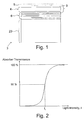
- Fig. 2 depicts an example of a characteristic curve of an absorber region 4 of a modulator 1 according to an advantageous embodiment of the present invention.
- the x-axis depicts the light intensity directed to the absorber region, and the ⁇ -axis depicts the transmission rate of the absorber region as a function of the light intensity. It can be seen that at low light intensities the transmission of the absorber is low, i.e. absorption is high. The transmission increases gradually with the increase in the light intensity.
- the transmission rate begins to increase more rapidly with the increase in the light intensity.
- the absorber 4 is saturated, wherein the transmission rate is at its maximum and further increase in light intensity does not substantially affect the transmission rate. Therefore, by modulating the pump laser 2 by a modulating signal 8 generated by a modulating signal source 24 ( Fig. 4 ) the light intensity of the pump laser 2 is changed according to changes in the modulating signal 8.
- the modulation effectiveness or contrast ratio
- the non-linearity of the quantum-well absorptive material is a function of the intensity of the incident radiation, pump wavelength, the absorption cross-section and material volume.
- the saturable absorber 4 can be included as an intrinsic region, into asymmetric Fabry-Pérot (ASFP) structure to further enhance the non-linear response of the modulator 1.
- ASFP Fabry-Pérot
- the ASFP saturable absorber 4 operates as a resonant or antiresonant absorber at a particular wavelength.
- the saturation intensity of a saturable absorber 4 is regulated by positioning absorber element (e.g. quantum wells) within the absorber cavity and by optimising the absorber volume (e.g. number of quantum wells).
- FIG. 1 An exemplary realization of the saturable absorber (modulation element) 3 is shown in cross-sectional view in Fig. 1 .
- the reflectivity of the bottom mirror 6 of the absorber has ideally 100 percent reflectivity for the signal light and transparent for the VCSEL pump light. However, in practice the reflectivity is slightly less than 100 percent.
- the modulator element 3 comprises a non-linear optical element 4 pumped optically by the radiation produced by the pump laser 2.
- the modulator element 3 is monolithically integrated with the pump laser 2 using vertical cavity configuration, which makes the coupling of the laser light into the modulator region 4 be efficient.
- the integration improves the important figures of merit of the intensity modulators, e.g., the "on/off” ratio and the transmission in the "on” state.
- the modulator comprises two optical beams: A first pump optical beam 10 carries the modulating signal in optical form for modulation/switching the signal light. A second optical beam 11 carries optical signal to be modulated; the signal light propagates substantially perpendicular to the surface of the device 1.
- the semiconductor modulator 1 induces VCSEL section 2 with a multiple quantum well design of the active region and a non-linear optical element 3 connected to the first pump optical beam 10 with surface-normal architecture in which the signal light 11, 16 propagates substantially perpendicular to the surface.
- the non-linear optical medium 4 of modulation element 3 is multiple quantum-well structure.
- the nonlinear element 3 of the modulator 1 is a surface reflection saturable absorber.
- the modulator region 4 includes a stack of semiconductor layers acting as Bragg reflector for signal beam 11.
- the signal wave to be modulated is injected through the input device aperture 12, passed the saturable absorber region 4 and reflected back by the Bragg reflector 6.
- the VCSEL 2 is a forward-biased diode. It comprises a gain medium 7, wherein an optical axis is defined between DBR mirrors 27.
- An exemplary realization of the electrically pumped VCSEL is shown in cross-sectional view in Fig. 3 .
- the VCSEL structure 2 of the present invention is not limited by the design presented in the description but other electrically pumped VCSELs having different electrical contact structure and modal guiding can also be implemented in the modulator.
- VCSEL technology has been researched for years as an alternative and less-costly light source for use in short-distance applications. Their smaller size, lower power, lower cost, and good reliability enabled their popularity to soar over the years.
- Commercial VCSELs run at 850 nm, although the market also began in the 980-nm range. Examples of the electrically pumped VCSEL can be found in opened literatures (for example E.
- Fig. 4 presents an example of an optical transmission system in which the semiconductor modulator 1 can be used for light modulation.
- the pump laser 2 receives an electrical pump signal and generates optical pump beam 10.
- the electrodes 14, 15 of the laser section is supplied with a modulating signal 8, which allows the laser section 2 to produce modulated laser emission.
- the modulated laser light passes through the absorber region 4 and modulates its transmission by saturating the absorption.
- the reflection of the modulator element 3 is increased or decreased by increasing or decreasing the intensity of the pump laser light 10.
- the modulator element 3 is exposed with an optical signal 11 to be modulated.
- This optical signal is generated by an optical signal source 18 from which the optical signal is coupled to an optical circulator 19 via an input fibre 20.
- the optical circulator directs the optical signal to the modulator 1 via a coupling fibre 21 for modulation.
- the modulated optical signal is reflected from the modulator element 3.
- the reflected signal acquires amplitude/intensity modulation since it is assumed that the absorption of the modulator element 3 is strongly saturated by the modulated laser light.
- the modulated light beam is directed back to the coupling fibre 21 in which the optical signal propagates back to the optical circulator 19.
- the modulated optical signal is directed to the output port fibre 22 for transmission.
- the quantum well structures of the laser 2 and modulator element 3 have the different parameters (e.g., bandgap). Generally, if the laser 2 wavelength is shorter than the bandgap wavelength of the modulator element 3, i.e. ⁇ pump ⁇ modulator , the laser light provides strong saturation of the absorption in the modulator element 3.
- the invention features a method for modulating an optical input 11, e.g., a laser beam, to provide a modulated optical output 16.
- the modulating VCSEL 2 generates a modulating beam 10 configured to strike the surface-normal saturable absorber 4.
- a surface-normal semiconductor saturable absorber 4 is irradiated with the optical input 11.
- a saturation intensity I s of the saturable absorber 4 and optical intensity of the integrated laser 2 can be selected such that the saturable absorber 4 is above the saturation intensity I s for the "ON" state, and it is below the saturation intensity I s for "OFF" state.
- the modulator When the modulating optical beam carriers a constant pump signal, either "ON” or “OFF”, the modulator operates as an optical switch.
- the modulating beam carries a modulating optical beam
- the output beam 16 reflected from the modulator section substantially perpendicularly to the DBR mirror 5, is modulated according to the modulating pump beam 10.
- the optimum overlap of the modulating beam 10 and output modulated beam 16 is determined by the monolithic structure of the device 1 which incorporates pump laser 2 and the absorption section 4 of the surface normal modulator 3 on the same substrate 17. Therefore, the modulating laser beam overlaps in the absorber region, where the modulation of the signal beam takes place, thus providing high modulation efficiency.
- the recovery time of the saturable absorber section 4 may be altered by using ion implantation.
- the modulator section 3 is constituted by the saturable absorption section 4, and the bottom mirror (distributed Bragg reflector) 6 having a high reflectivity for a wavelength of the signal modulated light formed on the top of said vertical-cavity surface-emitting pump laser 2.
- An electrically-pumped VCSEL is provided for converting an electrical signal into optical pump signal for modulation of the transmission of the modulator section in accordance with the amplitude of the converted electrical signal.
- a non-linear reflection-type saturable absorber is used for modulation/switching the optical signal in accordance with the amplitude of the electrical signal.
- the modulator section may comprise a top mirror 5 to exploit cavity effect for enhancing the modulation efficiency.
- the distributed Bragg reflector 6 of the modulator section 3 may be doped to conduct the injection current used for modulation of VCSEL 2.
Landscapes
- Physics & Mathematics (AREA)
- Condensed Matter Physics & Semiconductors (AREA)
- General Physics & Mathematics (AREA)
- Electromagnetism (AREA)
- Optics & Photonics (AREA)
- Semiconductor Lasers (AREA)
- Optical Modulation, Optical Deflection, Nonlinear Optics, Optical Demodulation, Optical Logic Elements (AREA)
Abstract
Description
- The present invention relates to modulation of optical light using semiconductor devices with surface-normal geometry, and more specifically, to enhancement of on/off ratio, or modulation contrast of surface-normal modulators. The present invention relates to a semiconductor modulator comprising a vertical-cavity surface-emitting laser to produce a pump optical beam emitting substantially perpendicular to a surface of the laser, and a modulator element for modulating an optical signal to produce a modulated optical signal. The present invention also relates to a method for producing a semiconductor modulator comprising a vertical-cavity surface-emitting laser to produce a pump optical beam emitting substantially perpendicular to a surface of the laser, and a modulator element for modulating an optical signal to produce a modulated optical signal.
- Optical modulators are key elements in optical technology used in such systems as optical interconnect systems. There is considerable interest in surface-normal modulators for high-speed, wide-band optical signal processing and interconnection technology. One attractive solution is based on an epitaxially grown semiconductor modulator structure, consisting of multiple quantum wells with an optical mirror or mirrors to form a modulator.
- In large-scale monolithic applications, where many components must be fabricated on a single wafer, it is essential to minimize the size of each component. Semiconductor surface normal modulators appear to be a promising solution because of their low power consumption and small size. Therefore, in comparison with waveguide type modulators, surface-normal modulators are most useful in applications where a fairly high density of outputs is desired. Another advantages of surface normal modulators are simplicity of the coupling of the light and fibre pigtailing and polarization insensitivity.
- A major problem with surface-normal modulators is low modulation contrast and efficiency, because the interaction length with an optical beam is limited to a few micrometers. To overcome shortcomings that arise due to the short interaction length, asymmetrical Fabry-Pérot (ASFP) structures have been used in surface-normal modulators. The ASFP modulator is composed of a pair of asymmetric mirrors separated by an active layer. The use of resonant structures strongly influences the device characteristics such as achievable modulation in a cavity, spectral bandwidth, sensitivity to changing ambient temperature and optical saturation. For instance, the bandwidth of such Fabry-Pérot structures is reduced as the mirror reflectivity increases.
- A variety of configurations of surface-normal modulators are being proposed to switch and modulate optical signals. Majority of the proposed surface-normal modulators are electrically-addressed devices whose operation is based on the Quantum-Confined Stark Effect (QCSE). They require the application of controlled amounts of electric field. This field is easily introduced by placing quantum wells in the intrinsic region of p-i-n diode. Several groups have realized hybrid optoelectronic ASFP devices by using the QCSE in multiple-quantum wells (MQWs). The device operation is based on the shift of excitonic absorption resonances in MQWs due to an applied electrical field. The changes in the device reflection (or transmission) then modulate the signal light. In all-optical modulator ultrashort pump pulses from the light source (possibly followed by an optical amplifier) irradiate the saturable absorber optical gate, and open it by the bleaching of the absorption. These devices use the strong non-linear absorption changes (i.e. absorption bleaching or saturation) in MQW structure, when excited optically with pump light. Signal light irradiates the same area of the device and, therefore, is encoded by the pump pulses. As a result, the data carried on the pump pulses are transferred to the signal light. Therefore, the method consists of modulating the saturable loss of the MQWs by optically pumping it above the bandgap by an external laser. This technique is attractive because it allows all-optical switching at ultrafast speed, however, it requires ultrashort pulse laser producing pump light for modulation the reflection/transmission of the optical gate.
- Some of the desirable characteristics of efficient optical modulators/switches are low chirp, low operation power, large contrast ratio, and high speed. In addition, modulators should ideally have desirable optical bandwidth.
- Vertical Cavity Surface Emitting Laser (VCSEL) diodes are semiconductor devices with light emission substantially perpendicular to the chip surface. They are highly attractive for applications in optoelectronics, since they offer several advantages compared to conventional edge-emitting (in-plane) laser diodes, such as low electric power consumption, capability of on-wafer testing, simplified fibre coupling and packaging, single-longitudinal-mode spectra, and suitability for 2D-array integration.
- The patent
US-5,574,738 discloses a GHz-range frequency-modulated laser based on manufacturable vertical cavity surface emitting lasers (VCSELs) and arrays. The laser exploits a saturable absorber contained within the VCSELs distributed Bragg reflector which may itself be adjusted during fabrication or in operation. Under controllable operating conditions, the saturable absorber will force the VCSEL to self-pulsate (in the GHz-regime) at rates related to the local intensity, absorption, lifetime, and carrier density of the saturable absorber. These conditions can be controlled in real time in one of three ways; first, by adjusting the injection current into the VCSEL itself; second, for a fixed VCSEL bias and the use of a third terminal, by modifying the carrier density within the saturable absorber via additional current injection; or third, the saturable absorber can be reverse-biased by simultaneously altering its absorption and carrier lifetime and thus carrier density. Additionally, the frequency response can be controlled in the fabrication process by affecting the location of the saturable absorber, the mirror design and cavity Q, and the laser size (and hence threshold current). - The patent publication
EP 0 618 651 discloses a surface emitting laser provided with a resonator having a structure in which a quantum well structure is formed in the non-doped Distributed Bragg Reflector mirror at the opposite side to a semiconductor substrate out of a pair of Distributed Bragg Reflector mirrors sandwiching the resonator. In the quantum well structure a light absorption wavelength region is changed due to the Wannier-Stark effect or quantum-confinement Stark effect. Therefore, by applying a modulation signal for changing the electric field in the DBR mirror, the reflection loss of the DBR mirror is changed and the optical output is modulated. - Particular interest with respect to fibre-optical communication systems exists for those VCSELs that are able to emit at wavelengths around 1.31 µm or 1.55 µm because of minimum dispersion or absorption in silica fibres, respectively. Eligible material systems of compound semiconductors are (Galn)(NAs) and GalnNAsSb(GaNAsSb) on GaAs substrate and on InP there are (InGaAl)As, (InGa)(AsP) and (AlGa)(AsSb) potential for both 1.31 µm and 1.55µm emitters.
- The realization of VCSELs with reasonable characteristics, however, suffers from several technological challenges related to the required materials, especially for InP-based devices in the 1.55 µm wavelength range:
- Low refractive index-contrast of Distributed Bragg Reflector (DBR) mirrors;
- Poor thermal conductivity of ternary- (quaternary-) compound semiconductor DBRs;
- Problematic light amplification performance at elevated temperatures;
- Selective Oxidation (of InAIAs) expected to cause material damage.
- GaAs-based dilute nitride and antimonide alloys are seen to challenge now dominating InP-based semiconductors in the long-wavelength (1.3-1.5 µm) device markets. GaAs would offer many advantages over InP. It would be cost-effective and robust and have higher thermal conductivity than InP, and would allow for the manufacture of monolithic vertical-cavity surface-emitting lasers (VCSELs) in a single epitaxial growth run. Since the conventional InP-based material system has inherent disadvantages like poor thermal property and lack of proper mirror materials, long-wavelength laser diode constructed on GaAs substrate is highly desirable. A new material of GalnNAs, which could be realized by addition of small amount of nitrogen into GalnAs composition, is one of the best candidates for active layer of GaAs-based long-wavelength laser diodes. Due to large energy discontinuity in conduction band, the temperature characteristics of GalnNAs/Ga(AI)As quantum well is expected to be excellent. Moreover, well established GaAs/AIGaAs distributed Bragg reflectors provide enough reflectivity and conductivity for vertical-cavity surface-emitting lasers (VCSELs). Lateral confinement of carrier and optical mode by oxide layer is also applicable to improve the device performances.
- The mixed group-III dilute nitrides, or substitutionally disordered Ga1-xInxNyAs1-y possess intriguing physical properties and great potential for applications in optoelectronics. Long-wavelength GalnNAs / GaAs lasers have already been demonstrated. The development and optimization of GaAs-based VCSELs in the near infrared region (1.3 µm -1.55 µm) includes techniques for current confinement such as blocking layers and selective oxidation, and also VCSELs with quantum dots as active material.
- It is an object of the present invention to use a laser light of the semiconductor injection laser integrated with multiple-quantum wells saturable absorber used in surface-normal configuration to modulate the reflection of the optical gate.
- It is another object of the invention to improve the modulation contrast of optically pumped surface-normal modulators.
- It is another object of the invention to increase the modulation efficiency of the optically pumped surface-normal modulators.
- Yet another object of this invention is to enable a number of applications, for example, the application of this technology in mode-locked lasers for repetition rate stabilization, in optical signal processing, in interconnection systems, etc.
- The device according to an advantageous embodiment of the invention comprises optically-controlled vertical-cavity modulator integrated monolithically with pump vertical-cavity surface-emitting laser. Molecular beam epitaxy (MBE) or metalorganic chemical vapor deposition (MOCVD) grown quantum well optoelectronic modulators in the GaInNAs / GaAs and GaInNAsSb(GaNAsSb) materials system can be used to meet the criteria for long-wavelength optical modulators.
- The device according to an advantageous embodiment of the present invention comprises a reflection-type modulator with surface-normal architecture in which the signal light propagates substantially perpendicular to the surface and exploiting pump optical beam from integrated vertical-cavity surface-emitting laser (VCSEL) for modulation/switching the signal light.
- The device concept exploits the integration of the surface-emitting vertical-cavity laser diode and surface-normal optical gate on the same substrate.
- More precisely, the semiconductor modulator according to the present invention is primarily characterized in that the modulator element is formed integrally on top of the emitting surface of the vertical-cavity surface-emitting laser, and that the modulator element comprises a first mirror, a second mirror, and an absorber region between the first and the second mirror, wherein at least the optical transmission of the absorber region is arranged to be varied by varying the intensity of the pump optical beam, that the intensity of the pump optical beam is arranged to be varied by varying the injection current to the vertical-cavity surface-emitting laser, and said optical signal, to be intensity modulated by the modulator element, is arranged to be externally applied substantially perpendicularly to the top surface of the modulator element. The method according to the present invention is primarily characterized in that the modulator element is formed on top of the emitting surface of the vertical-cavity surface-emitting laser, in which modulator element a first mirror, a second mirror, and an absorber region between the first and the second mirror are formed, wherein the method further comprises varying the injection current to the vertical-cavity surface-emitting laser to vary the intensity of the pump optical beam which varies at least the optical transmission of the absorber region, and said optical signal, to be intensity modulated by the modulator element, is externally applied substantially perpendicularly to the top surface of the modulator element.
- The present invention shows remarkable advantages over solutions of prior art. The pump VCSEL is directly modulated by modulating the injection current. Saturable absorber region is positioned on the top of the VCSEL structure and it is not affected by the injection current. Therefore, modulated laser light crosses the absorber region and modulates its transmission by saturating optically the absorption.
- There is no need for external light source to pump the absorption section of the modulator.
- In the following, the invention will be described with reference to the appended drawings, in which
- Fig. 1
- discloses in cross-sectional view an absorber region with distributed Bragg reflector of a semiconductor according to an advantageous embodiment of the present invention,
- Fig. 2
- depicts a characteristic of an absorber region of a semiconductor modulator according to an advantageous embodiment of the present invention,
- Fig. 3
- discloses in cross-sectional view a semiconductor modulator according to an advantageous embodiment of the present invention, and
- Fig. 4
- discloses an example of a transmission system in which the semiconductor modulator of the present invention can advantageously be implemented.
- The conceptual configuration of a
semiconductor modulator 1 according to an advantageous embodiment of the present invention is shown inFig. 3 . The basic parts of thesemiconductor modulator 1 include a vertical-cavity surface-emittinglaser 2, and amodulator element 3 comprising anabsorber region 4 with top and bottom mirrors 5, 6, preferably distributed Bragg reflectors shown inFig. 1 . Theabsorber region 4 and themirrors GaAs substrate 23. - The
pump laser 2 includes semiconductor gain medium 7 comprising quantum wells and distributed Bragg reflectors (DBRs) 27 as cavity mirrors. Thepump laser 2 allows for high-speed amplitude modulation of the laser beam by modulating the injection current of thelaser 2. - The
absorber region 4, which operates as an optical modulator, is optically connected with the laser cavity; it situates in the optical path of theoutput beam 10 of the laser. - The absorption rate of the
absorber region 4 can be varied by varying the intensity of the light that illuminates to theabsorber region 4. The characteristic curve of theabsorber region 4 is non-linear.Fig. 2 depicts an example of a characteristic curve of anabsorber region 4 of amodulator 1 according to an advantageous embodiment of the present invention. The x-axis depicts the light intensity directed to the absorber region, and the γ-axis depicts the transmission rate of the absorber region as a function of the light intensity. It can be seen that at low light intensities the transmission of the absorber is low, i.e. absorption is high. The transmission increases gradually with the increase in the light intensity. With light intensities near saturation intensity of the absorber (Is), the transmission rate begins to increase more rapidly with the increase in the light intensity. Eventually, at high light intensities, theabsorber 4 is saturated, wherein the transmission rate is at its maximum and further increase in light intensity does not substantially affect the transmission rate. Therefore, by modulating thepump laser 2 by a modulating signal 8 generated by a modulating signal source 24 (Fig. 4 ) the light intensity of thepump laser 2 is changed according to changes in the modulating signal 8. When the variations in the light intensity of thepump laser 2 are selected to vary around the abrupt part of the characteristic curve, the modulation effectiveness (or contrast ratio) is very high. - The non-linearity of the quantum-well absorptive material is a function of the intensity of the incident radiation, pump wavelength, the absorption cross-section and material volume.
- The
saturable absorber 4 can be included as an intrinsic region, into asymmetric Fabry-Pérot (ASFP) structure to further enhance the non-linear response of themodulator 1. TheASFP saturable absorber 4 operates as a resonant or antiresonant absorber at a particular wavelength. By taking appropriate values for the reflectivity of thetop reflector 5 of the ASFP, it is feasible to optimise the non-linearity and losses. The saturation intensity of asaturable absorber 4 is regulated by positioning absorber element (e.g. quantum wells) within the absorber cavity and by optimising the absorber volume (e.g. number of quantum wells). - An exemplary realization of the saturable absorber (modulation element) 3 is shown in cross-sectional view in
Fig. 1 . Theabsorber section 4, wherein said Fabry-Pérot étalon has a free spectral range and finesse that can be optimised by adjusting thickness of the spacer layer 9 (Fig. 1 ) and reflectivity of thetop mirror 5, e.g. distributed Bragg reflector. - The reflectivity of the
bottom mirror 6 of the absorber has ideally 100 percent reflectivity for the signal light and transparent for the VCSEL pump light. However, in practice the reflectivity is slightly less than 100 percent. - Preferably, the
modulator element 3 comprises a non-linearoptical element 4 pumped optically by the radiation produced by thepump laser 2. - Preferably, the
modulator element 3 is monolithically integrated with thepump laser 2 using vertical cavity configuration, which makes the coupling of the laser light into themodulator region 4 be efficient. The integration improves the important figures of merit of the intensity modulators, e.g., the "on/off" ratio and the transmission in the "on" state. - The modulator comprises two optical beams: A first pump
optical beam 10 carries the modulating signal in optical form for modulation/switching the signal light. A secondoptical beam 11 carries optical signal to be modulated; the signal light propagates substantially perpendicular to the surface of thedevice 1. - Preferably, the
semiconductor modulator 1 inducesVCSEL section 2 with a multiple quantum well design of the active region and a non-linearoptical element 3 connected to the first pumpoptical beam 10 with surface-normal architecture in which thesignal light - Preferably, the non-linear
optical medium 4 ofmodulation element 3 is multiple quantum-well structure. - Preferably, the
nonlinear element 3 of themodulator 1 is a surface reflection saturable absorber. - The
modulator region 4 includes a stack of semiconductor layers acting as Bragg reflector forsignal beam 11. - The signal wave to be modulated is injected through the
input device aperture 12, passed thesaturable absorber region 4 and reflected back by theBragg reflector 6. - The
VCSEL 2 is a forward-biased diode. It comprises a gain medium 7, wherein an optical axis is defined between DBR mirrors 27. An exemplary realization of the electrically pumped VCSEL is shown in cross-sectional view inFig. 3 . - It should be understood that the
VCSEL structure 2 of the present invention is not limited by the design presented in the description but other electrically pumped VCSELs having different electrical contact structure and modal guiding can also be implemented in the modulator. VCSEL technology has been researched for years as an alternative and less-costly light source for use in short-distance applications. Their smaller size, lower power, lower cost, and good reliability enabled their popularity to soar over the years. Commercial VCSELs run at 850 nm, although the market also began in the 980-nm range. Examples of the electrically pumped VCSEL can be found in opened literatures (for example E. Hall et al., "Electrically-pumped, single-epitaxial VCSELs at 1.55 µm with Sb-based mirrors", Electron. Lett., vol. 35, pp. 1337-1338, 1999, or Tchang-Hun et al., "Vertical resonator surface emission laser used in optical data communications systems comprises mirror structures, a light producing region, a semiconductor section", PATENT Numbers:DE10136334 ,Gb2370689 JP2002094180 -
Fig. 4 presents an example of an optical transmission system in which thesemiconductor modulator 1 can be used for light modulation. Thepump laser 2 receives an electrical pump signal and generatesoptical pump beam 10. Theelectrodes laser section 2 to produce modulated laser emission. The modulated laser light passes through theabsorber region 4 and modulates its transmission by saturating the absorption. The reflection of themodulator element 3 is increased or decreased by increasing or decreasing the intensity of thepump laser light 10. Themodulator element 3 is exposed with anoptical signal 11 to be modulated. This optical signal is generated by anoptical signal source 18 from which the optical signal is coupled to anoptical circulator 19 via aninput fibre 20. The optical circulator directs the optical signal to themodulator 1 via acoupling fibre 21 for modulation. The modulated optical signal is reflected from themodulator element 3. The reflected signal acquires amplitude/intensity modulation since it is assumed that the absorption of themodulator element 3 is strongly saturated by the modulated laser light. The modulated light beam is directed back to thecoupling fibre 21 in which the optical signal propagates back to theoptical circulator 19. By theoptical circulator 19 the modulated optical signal is directed to theoutput port fibre 22 for transmission. - The quantum well structures of the
laser 2 andmodulator element 3 have the different parameters (e.g., bandgap). Generally, if thelaser 2 wavelength is shorter than the bandgap wavelength of themodulator element 3, i.e. λpump<λmodulator, the laser light provides strong saturation of the absorption in themodulator element 3. - For example, for modulator operating near λmodulator=1.55 µm, the pump wavelength can conveniently be chosen in a range λpump=0.9-1.3 µm.
- In another aspect, the invention features a method for modulating an
optical input 11, e.g., a laser beam, to provide a modulatedoptical output 16. First, the modulatingVCSEL 2 generates amodulating beam 10 configured to strike the surface-normal saturable absorber 4. Second, a surface-normalsemiconductor saturable absorber 4 is irradiated with theoptical input 11. In the optically-pumped modulator, a saturation intensity Is of thesaturable absorber 4 and optical intensity of theintegrated laser 2, can be selected such that thesaturable absorber 4 is above the saturation intensity Is for the "ON" state, and it is below the saturation intensity Is for "OFF" state. When the modulating optical beam carriers a constant pump signal, either "ON" or "OFF", the modulator operates as an optical switch. When the modulating beam carries a modulating optical beam, theoutput beam 16, reflected from the modulator section substantially perpendicularly to theDBR mirror 5, is modulated according to the modulatingpump beam 10. The optimum overlap of themodulating beam 10 and output modulatedbeam 16 is determined by the monolithic structure of thedevice 1 which incorporatespump laser 2 and theabsorption section 4 of the surfacenormal modulator 3 on thesame substrate 17. Therefore, the modulating laser beam overlaps in the absorber region, where the modulation of the signal beam takes place, thus providing high modulation efficiency. - In another aspect, the recovery time of the
saturable absorber section 4 may be altered by using ion implantation. - The
modulator section 3 is constituted by thesaturable absorption section 4, and the bottom mirror (distributed Bragg reflector) 6 having a high reflectivity for a wavelength of the signal modulated light formed on the top of said vertical-cavity surface-emittingpump laser 2. - An electrically-pumped VCSEL is provided for converting an electrical signal into optical pump signal for modulation of the transmission of the modulator section in accordance with the amplitude of the converted electrical signal. In place of the optically-pumped modulator section, a non-linear reflection-type saturable absorber is used for modulation/switching the optical signal in accordance with the amplitude of the electrical signal.
- The modulator section may comprise a
top mirror 5 to exploit cavity effect for enhancing the modulation efficiency. - In an advantageous embodiment of the present invention the distributed
Bragg reflector 6 of themodulator section 3 may be doped to conduct the injection current used for modulation ofVCSEL 2. - It is obvious that the present invention is not limited solely to the above-presented embodiments, but it can be modified within the scope of the appended claims.
-
-
- G. D. Boyd et al., "5.5 GHz multiple quantum well reflection modulator", Electronics Letters, vol. 25, No. 9, pp. 558-560, 27 Apr. 1989.
- M. Whitehead et al., "High-contrast reflection modulation at normal incidence in asymmetric multiple quantum well Fabry-Perot structure", Electronics Letters, vol. 25, No. 9, pp. 566-568, 27 Apr. 1989.
- M. Chmielowski et al., "Quantum well vertical light modulator", IEEE Photonics Technology Letters, vol. 1, No. 4, pp. 77-79, 4 Apr. 1989.
- L. R. Brovelli et al., "Antiresonant Fabry-Perot quantum-well modulator to actively modelock and synchronise solid-state lasers", Electronics Letters, vol. 31, No. 5, pp. 381-382, 2 Mar. 1995.
- Hirano et al., "10 ps pulse all-optical discriminator using a high-speed saturable absorber optical gate", Electronics Letters, vol. 31, No. 9, pp. 736-737, 27 Apr. 1995.
- E. Lugagne Delpon et al., "Ultrafast excitonic saturable absorption in ion-implanted InGaAs/InAlAs multiple quantum wells", Applied Physics Letters, vol. 72, No. 7, pp. 759-761, 16 Feb. 1998.
- N. H. Bonadeo et al., "Passive harmonic mode-locked soliton fiber laser stabilized by an optically pumped saturable Bragg reflector", Optics Letters, vol. 25, No. 19, pp. 1421-1423, 1 Oct. 2000.
- M. Whitehead, and G, Parry, "High-contrast reflection modulation at normal incidence in asymmetric multiple quantum well Fabry-Perot structure", Electron. Lett., vol. 25, No. 9, pp. 566-568, 1989.
- A. Hirano, et al., "10Gbit/s RZ all-optical discrimination using refined saturable absorber optical gate", Electron. Lett., vol. 34, pp. 198-199, 1998.
- H. S. Loka, et al., "Ultrafast all-optical switching in an asymmetric Fabry-Pérot device using low-temperature-grown GaAs", IEEE Photon. Technol. Lett., vol. 10, pp. 1733-1735, 1998.
- J. Mangeney et al. "All-optical discrimination at 1.5 µm using ultrafast saturable absorber vertical cavity device", Electron. Lett., vol. 36, pp. 1486-1488, 2000.
- J. F. Heffernan et al., "All optical, high contrast absorptive modulation in an asymmetric Fabry-Perot étalon", Appl. Phys. Lett., vol. 58, pp. 2877-2879, 1991.
- N. Xiang, et al., " Broadband semiconductor saturable absorber mirror at 1.55 µm using Burstein-Moss shifted Ga0.47ln0.53As / InP distributed Bragg reflector", Electron. Lett., vol. 37, pp. 374-375, 2001.
- A. Isomäki, et al., "Amplified spontaneous noise suppression using non-linear vertical-cavity semiconductor gate", in Topical Meeting on Nonlinear Optics: Materials, Fundamentals and Applications, Hawaii, (Optical Society of America, Washington, D.C., 2002), paper MC2-1, pp. 31-33.
- E. Gouardes, et al., "GalnAs-GalnNAs-GalnAs intermediate layer structure for long wavelength lasers", IEEE Photon. Technol. Lett., vol. 14, pp. 896-898, 2002.
- N. Tansu, et al., "Temperature sensitivity of 1300-nm InGaAsN quantum-well lasers", IEEE Photon. Technol. Lett., vol. 14, pp. 1052-1054, 2002.
- R. J. Kaplar et al., "Deep-level defects in InGaAsN grown by molecular-beam epitaxy", Appl. Phys. Lett., vol. 80, pp. 4777-4779, 2002.
- E. Yoshida, et al., "A 40-GHz 0.9-ps regeneratively mode-locked fiber laser with a tuning range of 1530-1560 nm", IEEE Photon. Technol. Lett, vol. 11, pp. 1587-1589, 1999.
- O. G. Okhotnikov, et al., "Colliding-pulse harmonically mode-locked fiber laser", Appl. Phys. B, vol. 72, pp. 381-384, 2001.
- N. Xiang, et al., "Broadband semiconductor saturable absorber mirrors in the 1.55-µm wavelength range for pulse generation in fiber lasers", IEEE J. Quantum Electron., vol. 38, pp. 369-374, 2002.
- M. Guina, et al., "Harmonically mode-locked laser stabilized by semiconductor saturable absorber modulated with the residual pump", Appl. Phys. B., 74, July, 2002.
Claims (13)
- A semiconductor modulator (1) comprising a vertical-cavity surface-emitting laser (2) to produce a pump optical beam (10) emitting substantially perpendicular to a surface of the laser (2), and a modulator element (3) to be driven by said pump optical beam for modulating an optical signal (11) to produce an intensity modulated optical signal (16), wherein the modulator element (3) is formed integrally on top of the emitting surface of the vertical-cavity surface-emitting laser (2), and the modulator element (3) comprises a first (5) mirror, a second mirror (6), and an absorber region (4) between the first (5) and the second mirror (6), wherein at least the optical transmission of the absorber region (4) is arranged to be varied by varying the intensity of the pump optical beam (10), the intensity of the pump optical beam (10) is arranged to be varied by varying the injection current to the vertical-cavity surface-emitting laser (2), and said optical signal (11), to be intensity modulated by the modulator element, is arranged to be externally applied substantially perpendicularly to the top surface of the modulator element (3).
- A semiconductor modulator (1) according to claim 1, characterized in that the optical transmission of the modulator element (3) is nonlinearly dependent on the intensity of the pump optical beam (10).
- A semiconductor modulator (1) according to claim 1 or 2, characterized in that the second mirror (6) is a Distributed Bragg Reflector mirror having a high reflectivity at the wavelength of the modulated optical signal (16).
- A semiconductor modulator (1) according to any of claims 1 to 3, characterized in that the second mirror (6) of the modulator section (3) is doped to conduct the injection current used for modulation of pump laser (2).
- A semiconductor modulator (1) according to any of claims 1 to 4, characterized in that the modulator element (3) comprises GalnNAs /GaAs materials.
- A semiconductor modulator (1) according to any of claims 1 to 4, characterized in that the modulator element (3) comprises GalnNAsSb(GaNAsSb)/GaAs materials.
- A semiconductor modulator (1) according to any of claims 1 to 6, characterized in that it is arranged to be operating at wavelengths λ>1.3 µm.
- A semiconductor modulator (1) according to any of claims 1 to 7, characterized in that the first (5) mirror, the second mirror (6), and the absorber region (4) form a Fabry-Pérot étalon having a predetermined optical resonance frequency, and that the predetermined optical frequency is arranged to be occurred either at resonance or antiresonance of said Fabry-Pérot étalon.
- A semiconductor modulator (1) according to any of claims 1 to 8, characterized in that the vertical-cavity surface-emitting laser (2) and the modulator element (3) are monolithically integrated onto a same substrate.
- A method for producing a semiconductor modulator (1) comprising a vertical-cavity surface-emitting laser (2) to produce a pump optical beam (10) emitting substantially perpendicular to a surface of the laser (2), and a modulator element (3) to be driven by said pump optical beam for modulating an optical signal (11) to produce an intensity modulated optical signal (16), the wherein the modulator element (3) is formed integrally on top of the emitting surface of the vertical-cavity surface-emitting laser (2), in which modulator element (3) a first (5) mirror, a second mirror (6), and an absorber region (4) between the first (5) and the second mirror (6) are formed, wherein the method further comprises providing means for varying the injection current to the vertical-cavity surface-emitting laser (2) to vary the intensity of the pump optical beam (10) which varies at least the optical transmission of the absorber region (4), and providing means for externally applying said optical signal (11), to be intensity modulated by the modulator element, substantially perpendicularly to the top surface of the modulator element (3).
- A method according to claim 10, characterized in that in the production of the modulator element (3) GainNAs / GaAs materials are used.
- A method according to claim 10, characterized in that in the production of the modulator element (3) GalnNAsSb(GaNAsSb)/GaAs materials are used.
- A method according to claim 11 or 12, characterized in that the speed of the absorber region (4) is controlled by controlling density of defects by selecting material composition and growth condition.
Applications Claiming Priority (3)
| Application Number | Priority Date | Filing Date | Title |
|---|---|---|---|
| FI20021543A FI114351B (en) | 2002-08-28 | 2002-08-28 | Halvledaremodulator |
| FI20021543 | 2002-08-28 | ||
| PCT/FI2003/000623 WO2004021536A1 (en) | 2002-08-28 | 2003-08-27 | Vertical cavity surface emitting laser comprising a modulator monolithically integrated on top |
Publications (2)
| Publication Number | Publication Date |
|---|---|
| EP1547215A1 EP1547215A1 (en) | 2005-06-29 |
| EP1547215B1 true EP1547215B1 (en) | 2012-07-11 |
Family
ID=8564492
Family Applications (1)
| Application Number | Title | Priority Date | Filing Date |
|---|---|---|---|
| EP03790977A Expired - Lifetime EP1547215B1 (en) | 2002-08-28 | 2003-08-27 | Vertical cavity surface emitting laser comprising a modulator monolithically integrated on top |
Country Status (4)
| Country | Link |
|---|---|
| EP (1) | EP1547215B1 (en) |
| AU (1) | AU2003255548A1 (en) |
| FI (1) | FI114351B (en) |
| WO (1) | WO2004021536A1 (en) |
Cited By (1)
| Publication number | Priority date | Publication date | Assignee | Title |
|---|---|---|---|---|
| CN102654715A (en) * | 2011-12-27 | 2012-09-05 | 河海大学 | All-optical modulation device and method based on micro-nano GaAs optical waveguide |
Families Citing this family (1)
| Publication number | Priority date | Publication date | Assignee | Title |
|---|---|---|---|---|
| TWI405379B (en) * | 2010-09-14 | 2013-08-11 | True Light Corp | Vertical cavity surface emitting laser device and manufacturing method thereof |
Family Cites Families (3)
| Publication number | Priority date | Publication date | Assignee | Title |
|---|---|---|---|---|
| JPH06291406A (en) | 1993-03-31 | 1994-10-18 | Fujitsu Ltd | Surface emitting semiconductor laser |
| US5574738A (en) | 1995-06-07 | 1996-11-12 | Honeywell Inc. | Multi-gigahertz frequency-modulated vertical-cavity surface emitting laser |
| DE10004398A1 (en) * | 2000-02-02 | 2001-08-16 | Infineon Technologies Ag | VCSEL with monolithically integrated photodetector |
-
2002
- 2002-08-28 FI FI20021543A patent/FI114351B/en not_active IP Right Cessation
-
2003
- 2003-08-27 EP EP03790977A patent/EP1547215B1/en not_active Expired - Lifetime
- 2003-08-27 AU AU2003255548A patent/AU2003255548A1/en not_active Abandoned
- 2003-08-27 WO PCT/FI2003/000623 patent/WO2004021536A1/en not_active Ceased
Cited By (1)
| Publication number | Priority date | Publication date | Assignee | Title |
|---|---|---|---|---|
| CN102654715A (en) * | 2011-12-27 | 2012-09-05 | 河海大学 | All-optical modulation device and method based on micro-nano GaAs optical waveguide |
Also Published As
| Publication number | Publication date |
|---|---|
| AU2003255548A1 (en) | 2004-03-19 |
| FI20021543A0 (en) | 2002-08-28 |
| EP1547215A1 (en) | 2005-06-29 |
| WO2004021536A1 (en) | 2004-03-11 |
| FI114351B (en) | 2004-09-30 |
| FI20021543A7 (en) | 2004-02-29 |
Similar Documents
| Publication | Publication Date | Title |
|---|---|---|
| US5513204A (en) | Long wavelength, vertical cavity surface emitting laser with vertically integrated optical pump | |
| EP1499921B1 (en) | Optical modulator | |
| US7369583B2 (en) | Electrooptically wavelength-tunable resonant cavity optoelectronic device for high-speed data transfer | |
| US8290016B2 (en) | Optoelectric device for high-speed data transfer with electrooptically tunable stopband edge of a bragg-reflector | |
| US8218972B2 (en) | Wavelength division multiplexing system | |
| US6697413B2 (en) | Tunable vertical-cavity surface-emitting laser with tuning junction | |
| US5414726A (en) | Process and apparatus for the modulation and amplification of light beams | |
| US7580595B1 (en) | Data transmission optoelectric device | |
| US9054492B2 (en) | Light-emitting device having photon-lifetime modulation | |
| Chang et al. | Design and performance of high-speed VCSELs | |
| Van Eisden et al. | Optically decoupled loss modulation in a duo-cavity VCSEL | |
| JP2007219561A (en) | Semiconductor light emitting device | |
| WO2004021536A1 (en) | Vertical cavity surface emitting laser comprising a modulator monolithically integrated on top | |
| Clark et al. | Long-wavelength monolithic GaInNAs vertical-cavity optical amplifiers | |
| JP4820556B2 (en) | Vertical cavity surface emitting semiconductor laser device, optical transmission module, optical transmission device, and optical switching method | |
| Bjorlin et al. | Vertical-cavity amplifying modulator at 1.3 μm | |
| Hudgings et al. | Dynamic behavior and applications of a three-contact vertical-cavity surface-emitting laser | |
| Uenohara et al. | Long-wavelength multiple-quantum-well voltage-controlled bistable laser diodes | |
| Björlin et al. | 1.3 µm vertical-cavity amplifying switch | |
| Porzi et al. | Simultaneous dual-wavelength conversion with multiresonant saturable absorption vertical-cavity semiconductor gate | |
| Song et al. | 1.55 µm bottom-emitting InAlGaAs VCSELs with Al2O3/a-Si thin-film pairs as top mirror | |
| De Valicourt et al. | Dilute nitride vertical-cavity gate for all-optical logic at 1.3 µm | |
| Giannoulis et al. | Bringing high-performance GaInNAsSb/GaAs SOAs to true data applications | |
| Guina et al. | Saturable absorber intensity modulator | |
| Serkland et al. | VCSEL modulation using an integrated electro-absorption modulator |
Legal Events
| Date | Code | Title | Description |
|---|---|---|---|
| PUAI | Public reference made under article 153(3) epc to a published international application that has entered the european phase |
Free format text: ORIGINAL CODE: 0009012 |
|
| 17P | Request for examination filed |
Effective date: 20050321 |
|
| AK | Designated contracting states |
Kind code of ref document: A1 Designated state(s): AT BE BG CH CY CZ DE DK EE ES FI FR GB GR HU IE IT LI LU MC NL PT RO SE SI SK TR |
|
| AX | Request for extension of the european patent |
Extension state: AL LT LV MK |
|
| DAX | Request for extension of the european patent (deleted) | ||
| 17Q | First examination report despatched |
Effective date: 20101022 |
|
| GRAP | Despatch of communication of intention to grant a patent |
Free format text: ORIGINAL CODE: EPIDOSNIGR1 |
|
| GRAS | Grant fee paid |
Free format text: ORIGINAL CODE: EPIDOSNIGR3 |
|
| GRAA | (expected) grant |
Free format text: ORIGINAL CODE: 0009210 |
|
| AK | Designated contracting states |
Kind code of ref document: B1 Designated state(s): AT BE BG CH CY CZ DE DK EE ES FI FR GB GR HU IE IT LI LU MC NL PT RO SE SI SK TR |
|
| REG | Reference to a national code |
Ref country code: GB Ref legal event code: FG4D |
|
| REG | Reference to a national code |
Ref country code: CH Ref legal event code: EP |
|
| REG | Reference to a national code |
Ref country code: AT Ref legal event code: REF Ref document number: 566538 Country of ref document: AT Kind code of ref document: T Effective date: 20120715 |
|
| REG | Reference to a national code |
Ref country code: IE Ref legal event code: FG4D |
|
| REG | Reference to a national code |
Ref country code: DE Ref legal event code: R096 Ref document number: 60341535 Country of ref document: DE Effective date: 20120906 |
|
| PGFP | Annual fee paid to national office [announced via postgrant information from national office to epo] |
Ref country code: GB Payment date: 20120816 Year of fee payment: 10 |
|
| REG | Reference to a national code |
Ref country code: NL Ref legal event code: VDEP Effective date: 20120711 |
|
| REG | Reference to a national code |
Ref country code: AT Ref legal event code: MK05 Ref document number: 566538 Country of ref document: AT Kind code of ref document: T Effective date: 20120711 |
|
| PGFP | Annual fee paid to national office [announced via postgrant information from national office to epo] |
Ref country code: FR Payment date: 20120822 Year of fee payment: 10 Ref country code: DE Payment date: 20120816 Year of fee payment: 10 |
|
| PG25 | Lapsed in a contracting state [announced via postgrant information from national office to epo] |
Ref country code: CY Free format text: LAPSE BECAUSE OF FAILURE TO SUBMIT A TRANSLATION OF THE DESCRIPTION OR TO PAY THE FEE WITHIN THE PRESCRIBED TIME-LIMIT Effective date: 20120711 Ref country code: AT Free format text: LAPSE BECAUSE OF FAILURE TO SUBMIT A TRANSLATION OF THE DESCRIPTION OR TO PAY THE FEE WITHIN THE PRESCRIBED TIME-LIMIT Effective date: 20120711 Ref country code: BE Free format text: LAPSE BECAUSE OF FAILURE TO SUBMIT A TRANSLATION OF THE DESCRIPTION OR TO PAY THE FEE WITHIN THE PRESCRIBED TIME-LIMIT Effective date: 20120711 Ref country code: FI Free format text: LAPSE BECAUSE OF FAILURE TO SUBMIT A TRANSLATION OF THE DESCRIPTION OR TO PAY THE FEE WITHIN THE PRESCRIBED TIME-LIMIT Effective date: 20120711 |
|
| PG25 | Lapsed in a contracting state [announced via postgrant information from national office to epo] |
Ref country code: SI Free format text: LAPSE BECAUSE OF FAILURE TO SUBMIT A TRANSLATION OF THE DESCRIPTION OR TO PAY THE FEE WITHIN THE PRESCRIBED TIME-LIMIT Effective date: 20120711 Ref country code: PT Free format text: LAPSE BECAUSE OF FAILURE TO SUBMIT A TRANSLATION OF THE DESCRIPTION OR TO PAY THE FEE WITHIN THE PRESCRIBED TIME-LIMIT Effective date: 20121112 Ref country code: SE Free format text: LAPSE BECAUSE OF FAILURE TO SUBMIT A TRANSLATION OF THE DESCRIPTION OR TO PAY THE FEE WITHIN THE PRESCRIBED TIME-LIMIT Effective date: 20120711 Ref country code: GR Free format text: LAPSE BECAUSE OF FAILURE TO SUBMIT A TRANSLATION OF THE DESCRIPTION OR TO PAY THE FEE WITHIN THE PRESCRIBED TIME-LIMIT Effective date: 20121012 |
|
| REG | Reference to a national code |
Ref country code: CH Ref legal event code: PL |
|
| PG25 | Lapsed in a contracting state [announced via postgrant information from national office to epo] |
Ref country code: MC Free format text: LAPSE BECAUSE OF NON-PAYMENT OF DUE FEES Effective date: 20120831 Ref country code: NL Free format text: LAPSE BECAUSE OF FAILURE TO SUBMIT A TRANSLATION OF THE DESCRIPTION OR TO PAY THE FEE WITHIN THE PRESCRIBED TIME-LIMIT Effective date: 20120711 |
|
| PG25 | Lapsed in a contracting state [announced via postgrant information from national office to epo] |
Ref country code: RO Free format text: LAPSE BECAUSE OF FAILURE TO SUBMIT A TRANSLATION OF THE DESCRIPTION OR TO PAY THE FEE WITHIN THE PRESCRIBED TIME-LIMIT Effective date: 20120711 Ref country code: ES Free format text: LAPSE BECAUSE OF FAILURE TO SUBMIT A TRANSLATION OF THE DESCRIPTION OR TO PAY THE FEE WITHIN THE PRESCRIBED TIME-LIMIT Effective date: 20121022 Ref country code: CH Free format text: LAPSE BECAUSE OF NON-PAYMENT OF DUE FEES Effective date: 20120831 Ref country code: DK Free format text: LAPSE BECAUSE OF FAILURE TO SUBMIT A TRANSLATION OF THE DESCRIPTION OR TO PAY THE FEE WITHIN THE PRESCRIBED TIME-LIMIT Effective date: 20120711 Ref country code: CZ Free format text: LAPSE BECAUSE OF FAILURE TO SUBMIT A TRANSLATION OF THE DESCRIPTION OR TO PAY THE FEE WITHIN THE PRESCRIBED TIME-LIMIT Effective date: 20120711 Ref country code: LI Free format text: LAPSE BECAUSE OF NON-PAYMENT OF DUE FEES Effective date: 20120831 Ref country code: EE Free format text: LAPSE BECAUSE OF FAILURE TO SUBMIT A TRANSLATION OF THE DESCRIPTION OR TO PAY THE FEE WITHIN THE PRESCRIBED TIME-LIMIT Effective date: 20120711 |
|
| PLBE | No opposition filed within time limit |
Free format text: ORIGINAL CODE: 0009261 |
|
| STAA | Information on the status of an ep patent application or granted ep patent |
Free format text: STATUS: NO OPPOSITION FILED WITHIN TIME LIMIT |
|
| REG | Reference to a national code |
Ref country code: IE Ref legal event code: MM4A |
|
| PG25 | Lapsed in a contracting state [announced via postgrant information from national office to epo] |
Ref country code: SK Free format text: LAPSE BECAUSE OF FAILURE TO SUBMIT A TRANSLATION OF THE DESCRIPTION OR TO PAY THE FEE WITHIN THE PRESCRIBED TIME-LIMIT Effective date: 20120711 Ref country code: IT Free format text: LAPSE BECAUSE OF FAILURE TO SUBMIT A TRANSLATION OF THE DESCRIPTION OR TO PAY THE FEE WITHIN THE PRESCRIBED TIME-LIMIT Effective date: 20120711 |
|
| 26N | No opposition filed |
Effective date: 20130412 |
|
| PG25 | Lapsed in a contracting state [announced via postgrant information from national office to epo] |
Ref country code: BG Free format text: LAPSE BECAUSE OF FAILURE TO SUBMIT A TRANSLATION OF THE DESCRIPTION OR TO PAY THE FEE WITHIN THE PRESCRIBED TIME-LIMIT Effective date: 20121011 Ref country code: IE Free format text: LAPSE BECAUSE OF NON-PAYMENT OF DUE FEES Effective date: 20120827 |
|
| REG | Reference to a national code |
Ref country code: DE Ref legal event code: R097 Ref document number: 60341535 Country of ref document: DE Effective date: 20130412 |
|
| GBPC | Gb: european patent ceased through non-payment of renewal fee |
Effective date: 20130827 |
|
| PG25 | Lapsed in a contracting state [announced via postgrant information from national office to epo] |
Ref country code: TR Free format text: LAPSE BECAUSE OF FAILURE TO SUBMIT A TRANSLATION OF THE DESCRIPTION OR TO PAY THE FEE WITHIN THE PRESCRIBED TIME-LIMIT Effective date: 20120711 Ref country code: DE Free format text: LAPSE BECAUSE OF NON-PAYMENT OF DUE FEES Effective date: 20140301 |
|
| REG | Reference to a national code |
Ref country code: FR Ref legal event code: ST Effective date: 20140430 |
|
| PG25 | Lapsed in a contracting state [announced via postgrant information from national office to epo] |
Ref country code: LU Free format text: LAPSE BECAUSE OF NON-PAYMENT OF DUE FEES Effective date: 20120827 |
|
| REG | Reference to a national code |
Ref country code: DE Ref legal event code: R119 Ref document number: 60341535 Country of ref document: DE Effective date: 20140301 |
|
| PG25 | Lapsed in a contracting state [announced via postgrant information from national office to epo] |
Ref country code: GB Free format text: LAPSE BECAUSE OF NON-PAYMENT OF DUE FEES Effective date: 20130827 Ref country code: HU Free format text: LAPSE BECAUSE OF FAILURE TO SUBMIT A TRANSLATION OF THE DESCRIPTION OR TO PAY THE FEE WITHIN THE PRESCRIBED TIME-LIMIT Effective date: 20030827 |
|
| PG25 | Lapsed in a contracting state [announced via postgrant information from national office to epo] |
Ref country code: FR Free format text: LAPSE BECAUSE OF NON-PAYMENT OF DUE FEES Effective date: 20130902 |