EP1547167B1 - Superconducting quantum interference device - Google Patents
Superconducting quantum interference device Download PDFInfo
- Publication number
- EP1547167B1 EP1547167B1 EP03783833A EP03783833A EP1547167B1 EP 1547167 B1 EP1547167 B1 EP 1547167B1 EP 03783833 A EP03783833 A EP 03783833A EP 03783833 A EP03783833 A EP 03783833A EP 1547167 B1 EP1547167 B1 EP 1547167B1
- Authority
- EP
- European Patent Office
- Prior art keywords
- pick
- loop
- superconducting
- loops
- magnetic field
- Prior art date
- Legal status (The legal status is an assumption and is not a legal conclusion. Google has not performed a legal analysis and makes no representation as to the accuracy of the status listed.)
- Expired - Lifetime
Links
- 238000001514 detection method Methods 0.000 claims abstract description 19
- 238000000034 method Methods 0.000 claims abstract description 5
- 230000004907 flux Effects 0.000 claims description 45
- 239000000758 substrate Substances 0.000 claims description 39
- 229910000856 hastalloy Inorganic materials 0.000 claims description 17
- MCMNRKCIXSYSNV-UHFFFAOYSA-N Zirconium dioxide Chemical compound O=[Zr]=O MCMNRKCIXSYSNV-UHFFFAOYSA-N 0.000 claims description 8
- 239000004020 conductor Substances 0.000 claims description 8
- 241000238366 Cephalopoda Species 0.000 claims 1
- 239000010410 layer Substances 0.000 description 24
- 239000000463 material Substances 0.000 description 19
- 230000035945 sensitivity Effects 0.000 description 11
- 238000013461 design Methods 0.000 description 10
- IJGRMHOSHXDMSA-UHFFFAOYSA-N Atomic nitrogen Chemical compound N#N IJGRMHOSHXDMSA-UHFFFAOYSA-N 0.000 description 6
- 230000008878 coupling Effects 0.000 description 6
- 238000010168 coupling process Methods 0.000 description 6
- 238000005859 coupling reaction Methods 0.000 description 6
- 239000007788 liquid Substances 0.000 description 5
- 238000004519 manufacturing process Methods 0.000 description 4
- 238000011161 development Methods 0.000 description 3
- 230000018109 developmental process Effects 0.000 description 3
- 239000001307 helium Substances 0.000 description 3
- 229910052734 helium Inorganic materials 0.000 description 3
- SWQJXJOGLNCZEY-UHFFFAOYSA-N helium atom Chemical compound [He] SWQJXJOGLNCZEY-UHFFFAOYSA-N 0.000 description 3
- 238000007735 ion beam assisted deposition Methods 0.000 description 3
- 229910052757 nitrogen Inorganic materials 0.000 description 3
- BQCADISMDOOEFD-UHFFFAOYSA-N Silver Chemical compound [Ag] BQCADISMDOOEFD-UHFFFAOYSA-N 0.000 description 2
- 238000013459 approach Methods 0.000 description 2
- 230000005540 biological transmission Effects 0.000 description 2
- 230000015572 biosynthetic process Effects 0.000 description 2
- 238000005516 engineering process Methods 0.000 description 2
- 238000005259 measurement Methods 0.000 description 2
- 229910052709 silver Inorganic materials 0.000 description 2
- 239000004332 silver Substances 0.000 description 2
- 229910017415 LaAl2 Inorganic materials 0.000 description 1
- 229910002370 SrTiO3 Inorganic materials 0.000 description 1
- 230000001668 ameliorated effect Effects 0.000 description 1
- 238000005452 bending Methods 0.000 description 1
- 210000004556 brain Anatomy 0.000 description 1
- 239000000919 ceramic Substances 0.000 description 1
- 238000010276 construction Methods 0.000 description 1
- 239000002826 coolant Substances 0.000 description 1
- 239000013078 crystal Substances 0.000 description 1
- 230000007423 decrease Effects 0.000 description 1
- 230000007812 deficiency Effects 0.000 description 1
- 230000001419 dependent effect Effects 0.000 description 1
- 238000000151 deposition Methods 0.000 description 1
- 230000008021 deposition Effects 0.000 description 1
- 230000000694 effects Effects 0.000 description 1
- 238000005530 etching Methods 0.000 description 1
- 230000007717 exclusion Effects 0.000 description 1
- 230000001747 exhibiting effect Effects 0.000 description 1
- 238000002474 experimental method Methods 0.000 description 1
- 230000001939 inductive effect Effects 0.000 description 1
- 229910052500 inorganic mineral Inorganic materials 0.000 description 1
- 229910052751 metal Inorganic materials 0.000 description 1
- 239000002184 metal Substances 0.000 description 1
- 229910001092 metal group alloy Inorganic materials 0.000 description 1
- 239000011707 mineral Substances 0.000 description 1
- 238000012986 modification Methods 0.000 description 1
- 230000004048 modification Effects 0.000 description 1
- 238000005457 optimization Methods 0.000 description 1
- 210000000056 organ Anatomy 0.000 description 1
- 238000002161 passivation Methods 0.000 description 1
- 238000000059 patterning Methods 0.000 description 1
- 239000000843 powder Substances 0.000 description 1
- 239000011241 protective layer Substances 0.000 description 1
- 230000004044 response Effects 0.000 description 1
- 238000004088 simulation Methods 0.000 description 1
- 125000006850 spacer group Chemical group 0.000 description 1
- 239000002887 superconductor Substances 0.000 description 1
- 229910021521 yttrium barium copper oxide Inorganic materials 0.000 description 1
Images



Classifications
-
- G—PHYSICS
- G01—MEASURING; TESTING
- G01R—MEASURING ELECTRIC VARIABLES; MEASURING MAGNETIC VARIABLES
- G01R33/00—Arrangements or instruments for measuring magnetic variables
- G01R33/02—Measuring direction or magnitude of magnetic fields or magnetic flux
- G01R33/035—Measuring direction or magnitude of magnetic fields or magnetic flux using superconductive devices
- G01R33/0354—SQUIDS
- G01R33/0356—SQUIDS with flux feedback
-
- Y—GENERAL TAGGING OF NEW TECHNOLOGICAL DEVELOPMENTS; GENERAL TAGGING OF CROSS-SECTIONAL TECHNOLOGIES SPANNING OVER SEVERAL SECTIONS OF THE IPC; TECHNICAL SUBJECTS COVERED BY FORMER USPC CROSS-REFERENCE ART COLLECTIONS [XRACs] AND DIGESTS
- Y10—TECHNICAL SUBJECTS COVERED BY FORMER USPC
- Y10S—TECHNICAL SUBJECTS COVERED BY FORMER USPC CROSS-REFERENCE ART COLLECTIONS [XRACs] AND DIGESTS
- Y10S505/00—Superconductor technology: apparatus, material, process
- Y10S505/825—Apparatus per se, device per se, or process of making or operating same
- Y10S505/842—Measuring and testing
- Y10S505/843—Electrical
- Y10S505/845—Magnetometer
- Y10S505/846—Magnetometer using superconductive quantum interference device, i.e. squid
Definitions
- the present invention relates to superconducting devices having elements positioned in three dimensions, and in particular to high temperature superconducting devices having elements positioned in three dimensions.
- the invention particularly relates to high temperature superconducting axial gradiometers, which employ a gradiometric pick-up loop formed by etching a transformer loop structure on a flexible superconducting tape.
- the pick-up loop is preferably inductively coupled to a superconducting quantum interference device (SQUID) magnetometer.
- SQUID superconducting quantum interference device
- SQUIDs Superconducting Quantum Interference Devices
- Such SQUID sensors are becoming increasingly popular due to the capabilities of high sensitivity sensing in areas such as geophysical mineral prospecting and biological magnetic field detection, such as magnetic field emanations from the human brain or other human organs.
- HTS-SQUIDs can operate at or above 77K (-196°C) and hence can be cooled by relatively inexpensive liquid nitrogen, rather than requiring liquid helium as a coolant for operation at 4K (-269°C). Liquid nitrogen is also more convenient to use than liquid helium, allowing the system as a whole to be made in a compact form.
- HTS high-temperature superconducting
- HTS materials remain more difficult to use than the alternative low-temperature superconducting materials, and many design practices in low temperature helium cooled superconductors (LTS) cannot be implemented in HTS materials.
- LTS low temperature helium cooled superconductors
- the lack of HTS superconducting wires and the difficulty of forming superconducting connections in HTS materials means that the standard LTS design practice of forming gradiometer coils from superconducting wires, is not applicable in HTS materials.
- DC direct current
- the SQUID operates as a two-port device (SQUID amplifier) because the flux in the SQUID is derived from the current directly injected Into a pair of Input terminals.
- the current in the SQUID is proportional to the difference in the shielding currents induced in the pick-up loops in response to an external magnetic field gradient.
- the two pick-up loops are electrically in parallel, so one disadvantage of this topology is that even in a homogeneous field a large overall shielding current is induced in the outer perimeter of the pick-up loop structure with the potential to degrade noise performance through the associated production of large numbers of Abrikosov vortices In the superconducting film.
- HTS transverse gradiometers employs a planar pick-up loop structure that Is flip-chipped with a SQUID magnetometer to which it is inductively coupled.
- the flux transformer consists of a pair of pick-up loops, one of which is coupled to the SQUID magnetometer.
- the total effective magnetic area of the SQUID/loop combination can be made exactly opposite to that of the other loop of the flux transformer. Under these conditions the sensitivity to a homogeneous magnetic field vanishes but remains non-zero with respect to a magnetic field gradient.
- a second-order transverse gradiometer has also been Implemented using this approach.
- WO-A-00/57200 discloses a flexible tape transformer which measures magnetic susceptibility by positioning a powerful magnetic field source between the loops of patterned circuits.
- the different loops in each patterned circuit have significantly different inductances.
- the terms 'superconducting material', 'superconducting device' and the like are used to refer to a material or device which, in a certain state and at a certain temperature, is capable of exhibiting superconductivity. The use of such terms does not imply that the material or device exhibits superconductivity in all states or at all temperatures.
- the present invention provides an axial superconducting gradiometer as defined in claim 1.
- the present invention provides a method of forming an axial superconducting gradiometer in accordance with claim 8.
- the inherent characteristics of the two superconducting pick-up loops are likely to be significantly closer to being matched than would be the case for the characteristics of pick-up loops or devices formed on separate substrates.
- the error margin of such devices can be expected to be significantly smaller, and indeed, magnetic fields of up to 10 8 lower than the earth's magnetic field may be detected by some embodiments of the present invention.
- providing two superconducting pick-up loops on the common flexible substrate enables construction of magnetic field detection devices such as axial gradiometers which comprise only a single SQUID.
- Such circuits offer significant advantages over circuits requiring the extra complexity of providing a plurality of SQUIDs, in terms of both physical device manufacture and the device electrical characteristics.
- Superconducting tape has been developed primarily for power transmission applications. In early developments such tape was formed using powder In silver tube filled with one of the various ceramic HTS materials but more recently developments in tape technology have led to the ability to form YBCO films on both metal and insulating substrates with an intervening buffer layer.
- the common flexible substrate may comprise Hastelloy tape, preferably of 50 to 200 ⁇ m thickness.
- Hastelloy tape is also advantageous in that a pick-up loop of significantly larger area may be formed at significantly less cost, when compared to non-flexible crystalline substrates such as MgO, SrTiO 3 . LaAl 2 O 3 or the like.
- the common flexible substrate may comprise a partially or fully stabilised zirconia substrate, for example In very thin flexible sheet form, such as is provided under the name Ceraflex by MarkeTech International of 4750 Magnolia St, Port Townsend, WA, 98368, USA. Ceraflex has been found to possess improved noise properties over Hastelloy tape, enabling an SNR of a superconducting device formed over the Ceraflex substrate to be improved by perhaps 30% relative to Hastelloy tape.
- a biaxially aligned buffer layer such as yttria-stabilised zirconia (YSZ) is preferably formed over the common flexible substrate In order to improve biaxial alignment of a superconducting material from which the at least one superconducting pick up loop is formed.
- the buffer layer may be deposited by ion beam assisted deposition (IBAD), or by double ion beam assisted deposition (DIBAD), as set out in the present applicant's co-pending international Patent Application No. PCT/AU02/00696 published as WO-A-20021097462 .
- a magnetic field passing through the at least one pick up loop which induces a current In the at least one pick up loop may be detected by use of a SQUID.
- the SQUID may be formed on the common flexible substrate.
- the SQUID may be magnetically coupled to the at least one pick up loop by way of a flux transformer formed on the common flexible substrate, and by positioning the SQUID to allow coupling between the flux transformer and the SQUID.
- the SQUID may be mounted against the flux transformer in a "flip-chip" arrangement.
- the present inventors have recognised that it is possible to use flexible substrates, such as Hastelloy tapes or Ceraflex, to support a biaxially aligned buffer layer and thus to support a flexible superconducting circuit, formed over the buffer layer.
- such substrates may be used to support flexible superconducting circuits such as large area pick-up loops for magnetometers.
- the present invention extends the applications of superconducting tape utilising such flexible substrates to include use as a flexible superconducting medium for the fabrication of flexible superconducting circuits including gradiometer pick-up loops and flexible ground-planes for superconducting strip-lines. Further such applications include the formation of flexible superconducting wave-guides. In many such applications envisaged by the present Invention, even relatively short lengths of tape, of the order of a few hundred millimeters, would be sufficient.
- a smallest radius of curvature of the common flexible substrate should be controlled. This is due to the possibility of an overly tight curvature of the device causing damage to the polycrystalline flexible substrate, the biaxially aligned buffer layer, the crystalline superconducting layer or any other layer such as an overlying silver passivating layer.
- the minimum permissible radius of curvature of the device may vary.
- the tape may also be twisted In order to provide circuit elements in a third plane, for example, to provide elements in three orthogonal planes.
- a minimum radius of curvature or twist is preferably controlled In order to avoid damage to the device.
- the axial gradiometer includes a flux transformer.
- This may be formed by patterning an appropriate circuit using conventional resist techniques over the superconducting layer of the tape, which for Instance may be a YBCO layer formed over a biaxially aligned buffer layer of the flexible substrate.
- the flux transformer comprises two outer pick-up loops which are connected in series with a centrally located secondary loop via a pair of flexible strip-line conductors. A SQUID magnetometer is then "flip-chipped" over the secondary loop and separated from the secondary loop by means of Insulating spacers.
- two additional lengths of flexible superconducting tape are preferably used to cover the strip-line connectors between each outer pick up loop and the secondary loop.
- the additional lengths of flexible superconducting tape form a ground-plane.
- These additional lengths of flexible superconducting tape are preferably configured so as to serve three purposes. Firstly, such additional lengths of superconducting tape may serve to reduce unwanted shielding currents which might otherwise be Induced in the loop structure from the strip-line connectors, and secondly may serve to reduce the Inductance of the strip-line connectors.
- the effect of the strip-line inductance on the performance of the gradiometer is considered in more detail below.
- the additional superconducting tape ground-planes may, if necessary, be used to facilitate balancing or matching of the equivalent areas of the primary pick-up loops, for instance by sliding the additional superconducting covering ground tapes so as to expose an appropriate area of strip-line to the external field in a manner which balances the equivalent areas of the two outer pick up loops.
- the flexible substrate comprises a flexible tape made of a rolled metal alloy such as Hastelloy.
- a Ceraflex tape may alternatively be used.
- Ceraflex tapes have not been used for HTS applications, however it has been realised by the present inventors that Ceraflex tape provides improved noise performance over traditional tapes such as Hastelloy tape, improving the SNR of a superconducting device formed on the tape by perhaps 30% relative to Hastelloy tape.
- a buffer layer may be positioned between the substrate and the pick-up loops, for example to promote biaxial crystal alignment in superconducting material from which the pick-up loops are formed, and/or to isolate the superconducting material from the substrate.
- the buffer layer may comprise a biaxially aligned yttria-stabilised zirconia (YSZ) layer.
- the superconducting material may be YBa 2 Cu 3 O 7 (abbreviated as YBCO) or Bi 1.6 Pb 0.4 Sr 2 Ca 2 CU 3 O 10 (abbreviated as BSCCO).
- a protective layer such as an Ag layer can be provided over the superconducting material from which the pick-up loops are formed.
- a flux transformer is provided between the first and second pick-up loops in order to couple detected flux into a SQUID proximal to the flux transformer.
- a SQUID may be formed by conventional means on a separate substrate and “sandwich-mounted" against the flux transformer, in a "flip-chip” arrangement as described previously.
- a SQUID may be formed on the flexible substrate itself, by formation of a Josephson Junction, for example over a step edge etched into the substrate.
- HTS flexible tapes have mainly been considered for power transmission purposes.
- a relatively thin superconducting layer of perhaps 50-500 nm may be used in the present invention, as opposed to thicker power-carrying superconducting layers.
- FIG. 1 illustrates a high temperature superconducting (HTS) axial gradiometer 10 in accordance with an embodiment of both the first and fifth aspects of the present invention.
- the axial gradiometer comprises a flexible Hastelloy tape 11, providing a substrate for superconducting elements of the gradiometer.
- a buffer layer of YSZ has been grown over a surface of the Hastelloy tape to enhance biaxial alignment of YBCO formed over the YSZ.
- a first pick-up loop 12 formed of YBCO is provided proximal to one end of the tape 11, and a second pick-up loop 13 also formed of YBCO is provided proximal to an opposite end of the tape 11.
- the pick-up loops are connected to each other via strip-line connectors 14 and flux transformer 15 in a manner which substantially cancels out common-mode magnetic fields such as the earth's magnetic field, such that only a magnetic field which has a gradient between the first and second pick-up loops will cause current to flow in the superconducting YBCO elements 11, 12, 13, 14, 15.
- all superconducting elements of the gradiometer 10 can be fabricated on a single surface of the tape 11, and can be formed while positioned in a single plane using planar deposition technologies, see Fig 1b. Further, due to the flexibility of the Hastelloy tape, once fabricated the first and second pick-up loops 12, 13 can be axially aligned and positioned in substantially parallel planes a distance d apart.
- a SQUID may then be "sandwich mounted" to the Hastelloy tape 11 so as to be in close proximity to the flux transformer 15 and to maximise magnetic coupling between the SQUID and the flux transformer 15.
- the current circulating in the flux transformer 15 will induce another magnetic field, which will be coupled to the SQUID for detection,
- the present invention enables a HTS gradiometer to be constructed which does not suffer from the deficiencies associated with measurements relying on the measurements obtained by two different SQUIDs having differing inherent characteristics. Further, by using a flexible Hastelloy tape or the like, the present invention enables a single SQUID HTS gradiometer to be constructed, as flexible HTS circuits may be formed on such a substrate.
- FIG. 2 illustrates a magnetic field detection element 20, in accordance with an embodiment of the first aspect of the present invention.
- the magnetic field detection element 20 comprises a first pick up loop 21, a flux transformer 22, and a second pick up loop 23 not visible but of equal dimensions as pick up loop 21.
- the pick-up loops 21 and 23 and the flux transformer 22 are formed on a flexible substrate comprising a Ceraflex tape 25, A buffer layer of YSZ (not shown) is formed over the tape 25, and the pick-up loops 21, 23 and the flux transformer 22 are formed of YBCO deposited over the buffer layer. Tracks 24 connect pick-up loops 21, 23 with flux transformer 22.
- the flexible substrate 25 is arranged such that the pick-up loop 21 is positioned in a first plane which is substantially perpendicular to a second plane in which the second pick-up loop 23 is positioned. As indicated at 26, 27, the normals to the planes in which the pick-up loops 21, 23 are positioned meet at substantially 90 degrees.
- the magnetic detection element 20 is more likely to detect the magnetic dipole than prior art arrangements in which a pick-up loop is provided in one plane only. For example, if the magnetic dipole is aligned along axis 27, the field of the dipole will couple strongly through pick-up loop 23, but will not couple strongly into pick-up loop 21. If the magnetic dipole is aligned along axis 26, the field of the dipole will couple strongly into pick-up loop 21, but will not couple strongly into pick-up loop 23. If the dipole is aligned at 45 degrees to each axis 26, 27, the field of the dipole will couple with equal strength into each pick-up loop.
- FIG. 3 illustrates a magnetic field detection element 30 in accordance with another embodiment of the first aspect of the present invention.
- the element 30 comprises a first pick-up loop 31, a flux transformer 32 and a second pick-up loop 33.
- Pick-up loop 31 subtends an angle ⁇ of greater than 90 degrees. Consequently, a magnetic dipole aligned along an axis anywhere within angle ⁇ , will couple relatively strongly through pick-up loop 31.
- a magnetic dipole with an axis which is aligned anywhere within the angle (not shown) subtended by pick-up loop 33 will couple relatively strongly through pick-up loop 33.
- a stronger coupling will induce greater current in the pick-up loops 31, 33, and thus provide a stronger signal for detection by a SQUID sandwich mounted over flux transformer 32.
- FIG. 4(a) shows a first pick-up loop 42, a second pick-up loop 44 and a flux transformer 46.
- Each of the pick-up loops 42, 44 are directly linked to a secondary loop of the flux transformer 46 via respective strip conductors/connectors 48 and 50.
- Each of the pick-up loops 42, 44 and the secondary loop of the flux transformer 46 may each be formed of YBCO material. They are each fabricated on a flexible Hastelloy tape 52, shown in Figures 4(b) and 4(c) as shading.
- Figure 4(b shows the gradiometer 40 assembled prior to bending the strip conductor sections 48 and 50.
- Figure 4(c) shows a plan and side view of the complete axial gradiometer.
- a superconducting ground plane 56 covers each of the strip conductors 48 and 50.
- the ground planes 56 and strip conductors 48, 50 are shown curved with a radius r.
- the first pick-up loop 42 has internal dimensions d p1 , d p2 and external dimensions D p1 , D p2 .
- the second pick-up loop 44 has similar dimensions to that of the first pick-up loop 42 and the secondary loop of the flux transformer 46 has an internal length d s and external length D s .
- a SQUID may be sandwich mounted to the Hastelloy tape 52 of which a pick-up loop 54 is shown which is in close proximity to the secondary loop of the flux transformer 46 to establish a magnetic coupling therebetween.
- the magnetometer pick-up loop 54 has inductance L M and area A M
- the secondary loop of the flux transformer has inductance L s and effective area A s .
- Each of the pick-up loops 42 and 44 respectively have inductance L 1' L 2 and equivalent areas A 1 and A 2 respectively.
- FIG. 4 (c) Shown in Figure 4 (c) is the gradiometer having each of the pick-up loops 42 and 44 in parallel planes separated by distance d with the stripline connectors 48, 50 bent with a radial curvature r.
- Magnetic field B z is shown normal to the SQUID and flux transformer 46 whilst the magnetic field impinging on the first pick-up loop 42 is B x1 -B x +(d/2)g xx and the field impinging on the second pick-up loop 44 is B x2 -B x -(d/2)g xx .
- the strip-line sections are folded to form a "U" shape with the primary pick-up loops aligned on a common axis that is then perpendicular to the axis of the SQUID. Since the SQUID is oriented perpendicularly to the gradient pick-up loops, and assuming the orientation, this device is sensitive to both the first-order axial gradient, ⁇ B x / ⁇ x , and to the transverse component of the magnetic field B z . For applications in which the sensitivity to B z must be reduced, this can be achieved by appropriate design of the secondary loop and SQUID to ensure shielding of the magnetometer by currents induced in the secondary pick-up loop.
- the pick-up loop structure so formed is a series type. This decreases the magnitude of the shielding current which results from the components of any external homogeneous magnetic fields in the plane normal to the SQUID axis. Currents in the pick-up loops are induced only by a field gradient in the x - direction, mismatches between the magnetic equivalent areas of the primary loops, direct exposure of the strip-lines to the external field or by incorrect mutual inductance between the secondary loop and the SQUID.
- the axial gradiometer may also be mounted such that it is possible to rotate the gradiometer device either the SQUID and pick up loop together or the pick up loop with the SQUID stationary to achieve further improvements to the device usefulness. These improvements are:
- Rotation of axial gradiometers of both HTS axial gradiometers described here and LTS axial gradiometers provides the above enhancements.
- the magnetometer Since the magnetometer is coupled to the transformer secondary by a short-circuit superconducting loop, the flux in this loop is conserved with respect to changes in the external field.
- Equation (2) above is the widely accepted form for the equivalent area of a square washer [Ketchen1] in which the average values of the inner and outer dimensions of the rectangular loop are used.
- I m dg xx ⁇ p ⁇ ⁇ d p ⁇ D p ⁇ L s L m ⁇ [ 2 ⁇ L c + L s ⁇ 1 - ⁇ 2 + 2 ⁇ ⁇ 0 ⁇ d p ⁇ e - ⁇ ⁇ D p - d p / 2 ⁇ d p + 1.2 ] - 1
- Shown in Figures 5, 6, 7 are plots plotted as a function of d p and ⁇ for three different values of L c , namely 20 nH , 5 nH and 0.5 nH respectively.
- a device similar to that shown in Figure 3 may comprise a single pick-up loop only, subtending an arc in order to increase a range of magnetic dipole orientations which can be detected by the pick-up loop.
- such devices may comprise a SQUID fabricated on the tape itself In place of the flux transformer, such that the current of the pick-up loops flows directly into the SQUID for detection,
- the present invention may be applied in conjunction with the invention set out in the co-pending PCT application published as WO-A-2004/015435 .
- the present embodiments are, therefore, to be considered in all respects as illustrative and not restrictive.
Landscapes
- Physics & Mathematics (AREA)
- Condensed Matter Physics & Semiconductors (AREA)
- General Physics & Mathematics (AREA)
- Measuring Magnetic Variables (AREA)
- Superconductor Devices And Manufacturing Methods Thereof (AREA)
Abstract
Description
- The present invention relates to superconducting devices having elements positioned in three dimensions, and in particular to high temperature superconducting devices having elements positioned in three dimensions. The invention particularly relates to high temperature superconducting axial gradiometers, which employ a gradiometric pick-up loop formed by etching a transformer loop structure on a flexible superconducting tape. The pick-up loop is preferably inductively coupled to a superconducting quantum interference device (SQUID) magnetometer. In applications where the sensitivity to the magnetic field in the direction transverse to the gradiometer axis is problematic, the homogeneous background magnetic field can be reduced by matching the mutual inductance between the secondary loop of the flux transformer and.the magnetometer to establish a condition of shielding.
- Superconducting Quantum Interference Devices (SQUIDs) are often used as highly sensitive magnetic field sensors. Such SQUID sensors are becoming increasingly popular due to the capabilities of high sensitivity sensing in areas such as geophysical mineral prospecting and biological magnetic field detection, such as magnetic field emanations from the human brain or other human organs.
- With the advent of high critical temperature superconducting (HTS) materials such as YBa2Cu3Ox (YBCO), HTS-SQUIDs can operate at or above 77K (-196°C) and hence can be cooled by relatively inexpensive liquid nitrogen, rather than requiring liquid helium as a coolant for operation at 4K (-269°C). Liquid nitrogen is also more convenient to use than liquid helium, allowing the system as a whole to be made in a compact form.
- The use of high-temperature superconducting (HTS) materials for the fabrication of SQUID based magnetometers and gradiometers is now fairly well established (For example, W. Eidelloth, B. Oh, R. P. Robertazzi, W. J. Gallagher, R. H. Koch, Appl. Phys. Lett., 59, 3473 (1991); S. Knappe, D. Drung, T. Schurig, H. Koch, M. Klinger, J. Hinker, Cryogenics 32, 881, (1992); M. N, Keene, S. W. Goodyear, N. G. Chew, R. G. Humphreys, J. S. Satchell, J. A. Edwards, K. Lander, Appl. Phys. Lett. 64, 366 (1994); G. M. Daalmans, Appl. Supercond. 3, 399, (1995); M. I. Faley, U. Poppe, K. Urban, H.-J. Krause, H. Soltner, R. Hohmann, D. Lomparski, R. Kutzner, R. Wordenweber, H. Bousack, A. I. Braginski, V. Y. Slobodchikov, A. V. Gapelyuk, V. V. Khanin, Y.V. Maslennikov, IEEE Trans. Appl. Supercond., 7, 3702 (1997)). Despite the significant advantages which accrue from being able to operate at liquid nitrogen temperatures, HTS materials remain more difficult to use than the alternative low-temperature superconducting materials, and many design practices in low temperature helium cooled superconductors (LTS) cannot be implemented in HTS materials. In particular, the lack of HTS superconducting wires and the difficulty of forming superconducting connections in HTS materials means that the standard LTS design practice of forming gradiometer coils from superconducting wires, is not applicable in HTS materials.
- Designs for HTS gradiometers sensitive to the on-diagonal components, ∂Bi /∂xi (axial gradiometers), have been described (for example: R. H. Koch, J. R. Rozen, J. Z. Sun, W. J. Gallagher, Appl. Phys. Lett., 63, 403,(1993); H. J. M. ter Brake, N. Janssen, J. Flokstra, D. Veldehuis, H. Rogalla, IEEE Trans. Appl. Supercond., 7, 2545, (1997); J. Borgmann, P. David, G. Ockenfuss, R. Otto, J. Schubert, W. Zander, A.J. Braginski, Rev. Sci. Instrum. 68,2730,(1997) but these have been implemented only by means of electronic or software subtraction of the outputs of a pair of SQUID magnetometers which are generally positioned at fixed distances from each other on a common normal axis. These designs suffer from the disadvantage that both magnetometers must operate linearly in the full ambient field (often the earth's magnetic field). It is difficult to achieve good common-mode rejection (rejection of homogeneous fields) which is generally limited to an order of about 10-3 in most implementations. Furthermore, the achievable noise performance can be dependent upon the magnitude of the background homogeneous field; being determined by microphonics which arise from vibrations causing randomly varying misalignment of the axes of symmetry of the two SQUIDs.
- Some of these problems are ameliorated by the use of intrinsic gradiometer structures. Although several designs for intrinsic magnetic gradiometers utilising HTS films have been described in the literature these designs are sensitive only to the off-diagonal components of the first-order gradient tensor, ∂Bi /∂xj , i ≠ j (transverse gradiometers). These designs generally fall into one of two types. The first employs a "figure eight" topology in which the gradiometic pick-up loop structure consists of a pair of superconducting loops with a common conductor that is interrupted by a direct current (DC) SQUID. The SQUID operates as a two-port device (SQUID amplifier) because the flux in the SQUID is derived from the current directly injected Into a pair of Input terminals. Depending upon the matching of the inductances and equivalent magnetic areas of the gradiometer input loops the current in the SQUID is proportional to the difference in the shielding currents induced in the pick-up loops in response to an external magnetic field gradient. The two pick-up loops are electrically in parallel, so one disadvantage of this topology is that even in a homogeneous field a large overall shielding current is induced in the outer perimeter of the pick-up loop structure with the potential to degrade noise performance through the associated production of large numbers of Abrikosov vortices In the superconducting film.
- Another approach to the development of HTS transverse gradiometers employs a planar pick-up loop structure that Is flip-chipped with a SQUID magnetometer to which it is inductively coupled. In the first-order designs the flux transformer consists of a pair of pick-up loops, one of which is coupled to the SQUID magnetometer. By matching the mutual inductance between the SQUID and the loop, the total effective magnetic area of the SQUID/loop combination can be made exactly opposite to that of the other loop of the flux transformer. Under these conditions the sensitivity to a homogeneous magnetic field vanishes but remains non-zero with respect to a magnetic field gradient. A second-order transverse gradiometer has also been Implemented using this approach.
-
WO-A-00/57200 - Any discussion of documents, acts, materials, devices, articles or the like which has been included in the present specification is solely for the purpose of providing a context for the present invention. It is not to be taken as an admission that any or all of these matters form part of the prior art base or were common general knowledge in the field relevant to the present invention as it existed before the priority date of each claim of this application.
- Throughout this specification the word "comprise", or variations such as "comprises" or "comprising", will be understood to imply the Inclusion of a stated element, Integer or step, or group of elements, integers or steps, but not the exclusion of any other element, integer or step, or group of elements, integers or steps.
- Throughout this specification, the terms 'superconducting material', 'superconducting device' and the like are used to refer to a material or device which, in a certain state and at a certain temperature, is capable of exhibiting superconductivity. The use of such terms does not imply that the material or device exhibits superconductivity in all states or at all temperatures.
- According to a first aspect, the present invention provides an axial superconducting gradiometer as defined in
claim 1. - According to a second aspect, the present invention provides a method of forming an axial superconducting gradiometer in accordance with claim 8.
- The inherent characteristics of the two superconducting pick-up loops, such as critical current and effective area, are likely to be significantly closer to being matched than would be the case for the characteristics of pick-up loops or devices formed on separate substrates. Thus, the error margin of such devices can be expected to be significantly smaller, and indeed, magnetic fields of up to 108 lower than the earth's magnetic field may be detected by some embodiments of the present invention. Additionally, providing two superconducting pick-up loops on the common flexible substrate enables construction of magnetic field detection devices such as axial gradiometers which comprise only a single SQUID. Such circuits offer significant advantages over circuits requiring the extra complexity of providing a plurality of SQUIDs, in terms of both physical device manufacture and the device electrical characteristics.
- Superconducting tape has been developed primarily for power transmission applications. In early developments such tape was formed using powder In silver tube filled with one of the various ceramic HTS materials but more recently developments in tape technology have led to the ability to form YBCO films on both metal and insulating substrates with an intervening buffer layer.
- In preferred embodiments of the present invention, the common flexible substrate may comprise Hastelloy tape, preferably of 50 to 200 µm thickness. In addition to providing a common flexible substrate In accordance with the present Invention, Hastelloy tape is also advantageous in that a pick-up loop of significantly larger area may be formed at significantly less cost, when compared to non-flexible crystalline substrates such as MgO, SrTiO3. LaAl2O3 or the like. In alternate embodiments of the present invention, the common flexible substrate may comprise a partially or fully stabilised zirconia substrate, for example In very thin flexible sheet form, such as is provided under the name Ceraflex by MarkeTech International of 4750 Magnolia St, Port Townsend, WA, 98368, USA. Ceraflex has been found to possess improved noise properties over Hastelloy tape, enabling an SNR of a superconducting device formed over the Ceraflex substrate to be improved by perhaps 30% relative to Hastelloy tape.
- In embodiments of the present invention in which the common flexible substrate is a polycrystalline substrate such as Hastelloy or Ceraflex, a biaxially aligned buffer layer such as yttria-stabilised zirconia (YSZ) is preferably formed over the common flexible substrate In order to improve biaxial alignment of a superconducting material from which the at least one superconducting pick up loop is formed. The buffer layer may be deposited by ion beam assisted deposition (IBAD), or by double ion beam assisted deposition (DIBAD), as set out in the present applicant's co-pending international Patent Application No.
PCT/AU02/00696 WO-A-20021097462 - In embodiments of the present invention, a magnetic field passing through the at least one pick up loop which induces a current In the at least one pick up loop may be detected by use of a SQUID. The SQUID may be formed on the common flexible substrate. Alternatively the SQUID may be magnetically coupled to the at least one pick up loop by way of a flux transformer formed on the common flexible substrate, and by positioning the SQUID to allow coupling between the flux transformer and the SQUID. For example the SQUID may be mounted against the flux transformer in a "flip-chip" arrangement.
- The present inventors have recognised that it is possible to use flexible substrates, such as Hastelloy tapes or Ceraflex, to support a biaxially aligned buffer layer and thus to support a flexible superconducting circuit, formed over the buffer layer. For instance, such substrates may be used to support flexible superconducting circuits such as large area pick-up loops for magnetometers. Thus, the present invention extends the applications of superconducting tape utilising such flexible substrates to include use as a flexible superconducting medium for the fabrication of flexible superconducting circuits including gradiometer pick-up loops and flexible ground-planes for superconducting strip-lines. Further such applications include the formation of flexible superconducting wave-guides. In many such applications envisaged by the present Invention, even relatively short lengths of tape, of the order of a few hundred millimeters, would be sufficient.
- A smallest radius of curvature of the common flexible substrate should be controlled. This is due to the possibility of an overly tight curvature of the device causing damage to the polycrystalline flexible substrate, the biaxially aligned buffer layer, the crystalline superconducting layer or any other layer such as an overlying silver passivating layer. Depending on the materials from which the common flexible substrate, the buffer layer, the superconducting pick up loops, and any other layers such as a passivation layer are formed, the minimum permissible radius of curvature of the device may vary.
- The tape may also be twisted In order to provide circuit elements in a third plane, for example, to provide elements in three orthogonal planes. Once again, a minimum radius of curvature or twist is preferably controlled In order to avoid damage to the device.
- According to the invention, the axial gradiometer includes a flux transformer. This may be formed by patterning an appropriate circuit using conventional resist techniques over the superconducting layer of the tape, which for Instance may be a YBCO layer formed over a biaxially aligned buffer layer of the flexible substrate. In such embodiments, the flux transformer comprises two outer pick-up loops which are connected in series with a centrally located secondary loop via a pair of flexible strip-line conductors. A SQUID magnetometer is then "flip-chipped" over the secondary loop and separated from the secondary loop by means of Insulating spacers. In such embodiments, two additional lengths of flexible superconducting tape are preferably used to cover the strip-line connectors between each outer pick up loop and the secondary loop. With respect to the strip-line connectors, the additional lengths of flexible superconducting tape form a ground-plane. These additional lengths of flexible superconducting tape are preferably configured so as to serve three purposes. Firstly, such additional lengths of superconducting tape may serve to reduce unwanted shielding currents which might otherwise be Induced in the loop structure from the strip-line connectors, and secondly may serve to reduce the Inductance of the strip-line connectors. The effect of the strip-line inductance on the performance of the gradiometer is considered in more detail below. Finally, the additional superconducting tape ground-planes may, if necessary, be used to facilitate balancing or matching of the equivalent areas of the primary pick-up loops, for instance by sliding the additional superconducting covering ground tapes so as to expose an appropriate area of strip-line to the external field in a manner which balances the equivalent areas of the two outer pick up loops.
- In preferred embodiments of the present invention, the flexible substrate comprises a flexible tape made of a rolled metal alloy such as Hastelloy. Advantageously, a Ceraflex tape may alternatively be used. In the past, Ceraflex tapes have not been used for HTS applications, however it has been realised by the present inventors that Ceraflex tape provides improved noise performance over traditional tapes such as Hastelloy tape, improving the SNR of a superconducting device formed on the tape by perhaps 30% relative to Hastelloy tape.
- A buffer layer may be positioned between the substrate and the pick-up loops, for example to promote biaxial crystal alignment in superconducting material from which the pick-up loops are formed, and/or to isolate the superconducting material from the substrate. The buffer layer may comprise a biaxially aligned yttria-stabilised zirconia (YSZ) layer. The superconducting material may be YBa2Cu3O7 (abbreviated as YBCO) or Bi1.6Pb0.4Sr2Ca2CU3O10 (abbreviated as BSCCO). A protective layer such as an Ag layer can be provided over the superconducting material from which the pick-up loops are formed.
- In preferred embodiments of the fifth aspect of the invention, a flux transformer is provided between the first and second pick-up loops in order to couple detected flux into a SQUID proximal to the flux transformer. For example, a SQUID may be formed by conventional means on a separate substrate and "sandwich-mounted" against the flux transformer, in a "flip-chip" arrangement as described previously.
- Alternatively, a SQUID may be formed on the flexible substrate itself, by formation of a Josephson Junction, for example over a step edge etched into the substrate.
- To date, HTS flexible tapes have mainly been considered for power transmission purposes. Thus, it is envisaged that a relatively thin superconducting layer of perhaps 50-500 nm may be used in the present invention, as opposed to thicker power-carrying superconducting layers.
- By way of example only, preferred embodiments of the invention will be described with reference to the accompanying drawings, in which:
- Figure 1 illustrates a HTS gradiometer in accordance with a first embodiment of the present invention;
- Figure 2 Illustrates a magnetic field detection element in accordance with a second embodiment of the present invention;
- Figure 3 Illustrates a magnetic field detection element in accordance with a third embodiment of the present invention;
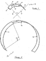
- Figures 4(a) to 4(c) illustrates a HTS.gradiometer In accordance with a fourth embodiment of the present invention;
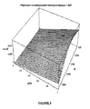
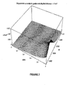
- Figure 5 illustrates the variation of the magnetometer current and gradient sensitivity with a stripline inductance of 20 nH;
- Figure 6 illustrates the variation of the magnetometer current and gradient sensitivity with a stripline inductance of 5 nH and
- Figure 7 Illustrates the variation of the magnetometer current and gradient sensitivity with a stripline inductance of 0.6 nH.
- Figure 1 illustrates a high temperature superconducting (HTS) axial gradiometer 10 in accordance with an embodiment of both the first and fifth aspects of the present invention. The axial gradiometer comprises a flexible Hastelloy tape 11, providing a substrate for superconducting elements of the gradiometer. A buffer layer of YSZ has been grown over a surface of the Hastelloy tape to enhance biaxial alignment of YBCO formed over the YSZ. A first pick-up
loop 12 formed of YBCO is provided proximal to one end of the tape 11, and a second pick-uploop 13 also formed of YBCO is provided proximal to an opposite end of the tape 11. The pick-up loops are connected to each other via strip-line connectors 14 andflux transformer 15 in a manner which substantially cancels out common-mode magnetic fields such as the earth's magnetic field, such that only a magnetic field which has a gradient between the first and second pick-up loops will cause current to flow in thesuperconducting YBCO elements - As can be seen, all superconducting elements of the gradiometer 10 can be fabricated on a single surface of the tape 11, and can be formed while positioned in a single plane using planar deposition technologies, see Fig 1b. Further, due to the flexibility of the Hastelloy tape, once fabricated the first and second pick-up
loops - A SQUID, not shown, may then be "sandwich mounted" to the Hastelloy tape 11 so as to be in close proximity to the
flux transformer 15 and to maximise magnetic coupling between the SQUID and theflux transformer 15. Thus, when current is induced in theflux transformer 15 by a magnetic field having a gradient between the first and second pick uploops flux transformer 15 will induce another magnetic field, which will be coupled to the SQUID for detection, - By using only a single SQUID, the present invention enables a HTS gradiometer to be constructed which does not suffer from the deficiencies associated with measurements relying on the measurements obtained by two different SQUIDs having differing inherent characteristics. Further, by using a flexible Hastelloy tape or the like, the present invention enables a single SQUID HTS gradiometer to be constructed, as flexible HTS circuits may be formed on such a substrate.
- Figure 2 illustrates a magnetic field detection element 20, in accordance with an embodiment of the first aspect of the present invention. The magnetic field detection element 20 comprises a first pick up
loop 21, aflux transformer 22, and a second pick uploop 23 not visible but of equal dimensions as pick uploop 21. The pick-uploops flux transformer 22 are formed on a flexible substrate comprising aCeraflex tape 25, A buffer layer of YSZ (not shown) is formed over thetape 25, and the pick-uploops flux transformer 22 are formed of YBCO deposited over the buffer layer.Tracks 24 connect pick-uploops flux transformer 22. - In accordance with the present invention, the
flexible substrate 25 is arranged such that the pick-uploop 21 is positioned in a first plane which is substantially perpendicular to a second plane in which the second pick-uploop 23 is positioned. As indicated at 26, 27, the normals to the planes in which the pick-uploops - Accordingly, when a magnetic dipole is positioned with random orientation where the
normals axis 27, the field of the dipole will couple strongly through pick-uploop 23, but will not couple strongly into pick-uploop 21. If the magnetic dipole is aligned alongaxis 26, the field of the dipole will couple strongly into pick-uploop 21, but will not couple strongly into pick-uploop 23. If the dipole is aligned at 45 degrees to eachaxis - When a field couples into one or both of pick-up
loops flux transformer 22, which is preferably designed so as to maximise magnetic coupling to a SQUID (not shown) which is to be sandwich mounted onto thetape 25. Detection of the magnetic field of the dipole can then be carried out with high sensitivity by the SQUID. - Figure 3 illustrates a magnetic
field detection element 30 in accordance with another embodiment of the first aspect of the present invention. Theelement 30 comprises a first pick-uploop 31, aflux transformer 32 and a second pick-uploop 33. Pick-uploop 31 subtends an angle θ of greater than 90 degrees. Consequently, a magnetic dipole aligned along an axis anywhere within angle θ, will couple relatively strongly through pick-uploop 31. Similarly, a magnetic dipole with an axis which is aligned anywhere within the angle (not shown) subtended by pick-uploop 33 will couple relatively strongly through pick-uploop 33. A stronger coupling will induce greater current in the pick-uploops flux transformer 32. - According to a further embodiment there is shown in Figures 4(a) to 4(c) an
HTS gradiometer 40. Figure 4(a) shows a first pick-uploop 42, a second pick-uploop 44 and aflux transformer 46. Each of the pick-uploops flux transformer 46 via respective strip conductors/connectors loops flux transformer 46 may each be formed of YBCO material. They are each fabricated on aflexible Hastelloy tape 52, shown in Figures 4(b) and 4(c) as shading. Figure 4(b shows thegradiometer 40 assembled prior to bending thestrip conductor sections superconducting ground plane 56 covers each of thestrip conductors strip conductors - The first pick-up
loop 42 has internal dimensions dp1, dp2 and external dimensions Dp1, Dp2. The second pick-uploop 44 has similar dimensions to that of the first pick-uploop 42 and the secondary loop of theflux transformer 46 has an internal length ds and external length Ds. A SQUID may be sandwich mounted to theHastelloy tape 52 of which a pick-uploop 54 is shown which is in close proximity to the secondary loop of theflux transformer 46 to establish a magnetic coupling therebetween. The magnetometer pick-uploop 54 has inductance LM and area AM, the secondary loop of the flux transformer has inductance Ls and effective area As. Each of the pick-uploops - Shown in Figure 4 (c) is the gradiometer having each of the pick-up
loops stripline connectors flux transformer 46 whilst the magnetic field impinging on the first pick-uploop 42 is Bx1-Bx+(d/2)gxx and the field impinging on the second pick-uploop 44 is Bx2-Bx-(d/2)gxx. Thus when current is induced in the secondary loop of theflux transformer 46 by magnetic field having a gradient between the first and second pick-uploops loop 54 of the SQUID thereby inducing a further current which is detected by the SQUID. - With regard to the design of the axial gradiometer, the strip-line sections are folded to form a "U" shape with the primary pick-up loops aligned on a common axis that is then perpendicular to the axis of the SQUID. Since the SQUID is oriented perpendicularly to the gradient pick-up loops, and assuming the orientation, this device is sensitive to both the first-order axial gradient, ∂Bx /∂ x , and to the transverse component of the magnetic field Bz. For applications in which the sensitivity to Bz must be reduced, this can be achieved by appropriate design of the secondary loop and SQUID to ensure shielding of the magnetometer by currents induced in the secondary pick-up loop. The pick-up loop structure so formed is a series type. This decreases the magnitude of the shielding current which results from the components of any external homogeneous magnetic fields in the plane normal to the SQUID axis. Currents in the pick-up loops are induced only by a field gradient in the x- direction, mismatches between the magnetic equivalent areas of the primary loops, direct exposure of the strip-lines to the external field or by incorrect mutual inductance between the secondary loop and the SQUID.
- The axial gradiometer may also be mounted such that it is possible to rotate the gradiometer device either the SQUID and pick up loop together or the pick up loop with the SQUID stationary to achieve further improvements to the device usefulness. These improvements are:
- true value of the gradient field and magnetic field,
- greatly enhanced common mode rejection of homogeneous fields
- real time information of the condition of the SQUID operation
- if three axial gradiometers are mounted near orthogonally or orthogonally, jointly they provide all five unique components of the first order gradient tensor and the three components of the total field
- these improvements can be achieved without the need to attain perfect balance usually achieved by the physical alignment of the pick up loops of the flexible tape.
- Rotation of axial gradiometers of both HTS axial gradiometers described here and LTS axial gradiometers provides the above enhancements.
- Assume a lumped inductance model with all mutual inductances regarded as negligible other than the mutual inductance, M, between the secondary loop of the flux transformer and the magnetometer. In what follows it is assumed that the magnetometer employed is a SQUID based directly-coupled magnetometer. In this type of magnetometer a superconducting pick-up loop is used to sense the external magnetic field, The inductance and equivalent area of the magnetometer pick-up loop will be denoted Lm and Am respectively. Currents induced in this loop are injected into a SQUID amplifier that has a geometry optimized for minimum flux noise, A magnetometer of this type is assumed for two reasons. Firstly these devices currently provide the best sensitivity possible from HTSC SQUID based magnetometers, and are therefore likely candidates for a practical device. Secondarily, as will be seen below, the alternative choice of a DC or RF SQUID with a flux-focussing washer, can be regarded as a special case of the present theory.
- Since the magnetometer is coupled to the transformer secondary by a short-circuit superconducting loop, the flux in this loop is conserved with respect to changes in the external field. The total flux in the magnetometer pick-up loop is the sum of the fluxes due to the external field, its own shielding current and the flux coupled via the mutual inductance M from the current I, in the secondary loop of the transformer. Assuming, without loss of generality, that the device is zero field cooled (Z.F.C), this sum vanishes, i.e,

- The flux transformer is also a shorted superconducting loop, so once again assuming it is Z.F.C

where L is the total inductance of the transformer, i.e.:
Lk, Ak denote the inductance and equivalent area of the primary loop k,
(k = 1,2), Lc in the inductance of each of the strip-lines and Ls is the inductance of the secondary loop. - Solving equations and simultaneously gives for the magnetometer current

where A 1 = A 2 ≙ A, and
- This can be re-written in terms of the coupling constant α by use of the standard relation


where
- If the external field is homogeneous gxx = 0 and equation becomes


- If is fulfilled, equations and for the magnetometer current, become simply

- To study the behaviour of equation (1), note that in general both A, the equivalent area of the primary loops of the transformer, and Lp depend upon the dimensions of the primary loop. As far as the applicant is aware exact forms for these relations do not exist for either square or rectangular superconducting structures and it is usual to resort to empirical formulae which are motivated either by experiment or numerical simulation. The following empirical relations will be used in which dp ≙ (d 1+d 2)/2 and

where 0.8 ≲ γ p ≲ 1 is approximately constant,

- Equation (2) above is the widely accepted form for the equivalent area of a square washer [Ketchen1] in which the average values of the inner and outer dimensions of the rectangular loop are used.
Use of these relations in equation (1) above gives
Shown in Figures 5, 6, 7 are plots plotted as a function of dp and α for three different values of Lc , namely 20nH, 5nH and 0.5nH respectively. Other parameters are set as follows: Dp = 0.01, γp = 0.9, Lm = 5nH, Ls = 10nH. - It will be appreciated by persons skilled In the art that numerous variations and/or modifications may be made to the invention as shown in the specific embodiments. For example, a device similar to that shown in Figure 3 may comprise a single pick-up loop only, subtending an arc in order to increase a range of magnetic dipole orientations which can be detected by the pick-up loop. Further, such devices may comprise a SQUID fabricated on the tape itself In place of the flux transformer, such that the current of the pick-up loops flows directly into the SQUID for detection, Furthermore, the present invention may be applied in conjunction with the invention set out in the co-pending PCT application published as
WO-A-2004/015435 . The present embodiments are, therefore, to be considered in all respects as illustrative and not restrictive.
Claims (8)
- An axial superconducting gradiometer (10, 20, 30, 40) comprising:a first pick-up loop (12, 21, 31, 42) defining and substantially residing in a first nominal plane; anda second pick-up loop (13, 23, 33, 44) defining and substantially residing in a second nominal plane;wherein the first pick-up loop (12, 21, 31, 42) and the second pick-up loop (13, 23, 33,44) are formed on a common flexible substrate (11, 25, 52), wherein the first nominal plane and the second nominal plane are substantially parallel, and wherein the first nominal plane and the second nominal plane are sufficiently spaced apart to allow the first pick-up loop (12, 21, 31, 42) and the second pick-up loop (13, 23, 33, 44) to act to distinguish local magnetic fields from background magnetic fields; and
a superconducting flux transformer (15, 22, 32, 46) patterned on the common flexible substrate (11, 25, 52) and inductively coupled to a detection means for detecting current induced in either the first (12, 21, 31, 42) or second (13, 23, 33, 44) pick-up loops as a result of a magnetic field passing through the first (12, 21, 31, 42) or second (13, 23, 33, 44) pick-up loops. - An axial superconducting gradiometer (10, 20, 30, 40) according to claim 1 further comprising a flexible strip-line conductor (14, 24, 48, 50) connecting each of the first (12, 21, 31, 42) and second (13, 23, 33, 44) pick-up loops to the flux transformer (15, 22, 32, 46).
- An axial superconducting gradiometer (40) according to claim 2, wherein an additional length of flexible superconducting tape (56) covers each of the strip-line conductors (48, 50) forming a ground plane.
- An axial superconducting magnetic field detection element (10, 20, 30, 40) according to any one of claims 1 to 3, wherein the common flexible substrate (11, 25, 52) is selected from Hastelloy tape and a partially or fully stabilised zirconia substrate, such as Ceraflex.
- An axial superconducting magnetic field detection element according to any one of claims 1 to 4 further comprising a SQUID for detecting current induced in the flux transformer (15, 22, 32, 46) as a result of a magnetic field passing though the first and second pick-up loops (12, 13; 21, 23; 31, 33; 42, 44).
- An axial superconducting magnetic field detection element according to any one of claims 1 to 5, wherein a minimum radius of curvature or twist of the common flexible substrate (11, 25, 52) is controlled in order to avoid damage to the gradiometer.
- An axial superconducting magnetic field detection element according to any one of claims 1 to 6, wherein the common flexible substrate (11, 25, 52) is twisted in order to provide circuit elements, such as a superconducting pick-up loop, in a third plane.
- A method of forming an axial superconducting gradiometer (10, 20, 30, 40), the method comprising:forming a first pick-up loop (12, 21, 31, 42) defining and substantially residing in a first nominal plane; andforming a second pick-up loop (13, 23, 33, 44) defining and substantially residing in a second nominal plane, wherein the first pick-up loop (12, 21, 31, 42) and the second pick-up loop (13, 23, 33, 44) are formed on a common flexible substrate (11, 25, 52), wherein the first nominal plane and the second nominal plane are sufficiently spaced apart to allow the first pick-up loop (12, 21, 31, 42) and the second pick-up loop (13, 23, 33, 44) to act to distinguish local magnetic fields from background magnetic fields; andforming a superconducting flux transformer (15, 22, 32, 46) patterned on the common flexible substrate and inductively coupled to a detection means for detecting current induced in either the first or second pick-up loops (12, 13; 21, 23; 31, 33; 42, 44) as a result of a magnetic field passing through the first or second pick-up loops (12, 13; 21, 23; 31, 33; 42, 44).
Applications Claiming Priority (3)
| Application Number | Priority Date | Filing Date | Title |
|---|---|---|---|
| AU2002950624 | 2002-08-07 | ||
| AU2002950624A AU2002950624A0 (en) | 2002-08-07 | 2002-08-07 | Superconducting quantum interference device |
| PCT/AU2003/000997 WO2004015788A1 (en) | 2002-08-07 | 2003-08-07 | Superconducting quantum interference device |
Publications (3)
| Publication Number | Publication Date |
|---|---|
| EP1547167A1 EP1547167A1 (en) | 2005-06-29 |
| EP1547167A4 EP1547167A4 (en) | 2005-12-21 |
| EP1547167B1 true EP1547167B1 (en) | 2007-06-13 |
Family
ID=27809718
Family Applications (2)
| Application Number | Title | Priority Date | Filing Date |
|---|---|---|---|
| EP03783833A Expired - Lifetime EP1547167B1 (en) | 2002-08-07 | 2003-08-07 | Superconducting quantum interference device |
| EP03783835A Expired - Lifetime EP1527349B1 (en) | 2002-08-07 | 2003-08-07 | Method and apparatus for magnetic field detection |
Family Applications After (1)
| Application Number | Title | Priority Date | Filing Date |
|---|---|---|---|
| EP03783835A Expired - Lifetime EP1527349B1 (en) | 2002-08-07 | 2003-08-07 | Method and apparatus for magnetic field detection |
Country Status (8)
| Country | Link |
|---|---|
| US (2) | US7508202B2 (en) |
| EP (2) | EP1547167B1 (en) |
| JP (2) | JP2005534929A (en) |
| AT (2) | ATE512368T1 (en) |
| AU (1) | AU2002950624A0 (en) |
| CA (3) | CA2829934C (en) |
| DE (1) | DE60314431T2 (en) |
| WO (2) | WO2004015435A1 (en) |
Cited By (1)
| Publication number | Priority date | Publication date | Assignee | Title |
|---|---|---|---|---|
| DE102013016739A1 (en) | 2012-10-08 | 2014-04-10 | Institut Für Photonische Technologien E.V. | Superconducting quantum interference device-based sensor assembly for absolute measurement of magnetic flux, has superconducting quantum interference devices, which are arranged, such that similar measuring of magnetic field is performed |
Families Citing this family (23)
| Publication number | Priority date | Publication date | Assignee | Title |
|---|---|---|---|---|
| US8125220B2 (en) | 2005-12-22 | 2012-02-28 | Koninklijke Philips Electronics N.V. | Magnetic induction tomography system and method |
| US7925117B2 (en) * | 2006-06-27 | 2011-04-12 | Honeywell International Inc. | Fusion of sensor data and synthetic data to form an integrated image |
| AU2007288138A1 (en) * | 2006-08-25 | 2008-02-28 | Commonwealth Scientific And Industrial Research Organisation | Method and apparatus for nano-scale SQUID |
| EP2231010B1 (en) * | 2007-12-14 | 2013-01-16 | Sophysa | Locator, device and method for electronically locating and reading the setting of an adjustable valve |
| US8179135B2 (en) * | 2008-01-28 | 2012-05-15 | California Institute Of Technology | Low field electron paramagnetic resonance imaging with SQUID detection |
| US8222899B2 (en) * | 2009-04-21 | 2012-07-17 | Herng-Er Horng | Squid detected nuclear magnetic resonance and imaging at ultra-weak fields |
| JP5492600B2 (en) * | 2010-02-26 | 2014-05-14 | 富士通株式会社 | Magnetic flux transformer and coaxial three-dimensional gradiometer |
| WO2012068493A1 (en) * | 2010-11-18 | 2012-05-24 | Johns Hopkins University | Magnetoencephalography system and method for 3d localization and tracking of electrical activity in brain |
| US8693204B2 (en) * | 2011-01-10 | 2014-04-08 | Apple Inc. | Electronic devices having multi-purpose cowling structures and a compass mounted on a flex circuit |
| US8887587B2 (en) * | 2012-07-11 | 2014-11-18 | Deutsches Zentrum Fuer Luft- Und Raumfahrt E.V. | Measurement device |
| US9784774B2 (en) | 2014-01-06 | 2017-10-10 | The Nielsen Company (Us), Llc | Methods and apparatus to determine an operational status of a device |
| US9746346B2 (en) | 2014-09-10 | 2017-08-29 | Infineon Technologies Ag | Linear position and rotary position magnetic sensors, systems, and methods |
| US9863788B2 (en) * | 2014-09-10 | 2018-01-09 | Infineon Technologies Ag | Linear position and rotary position magnetic sensors, systems, and methods |
| US9917216B2 (en) * | 2014-11-04 | 2018-03-13 | International Business Machines Corporation | Flexible kesterite photovoltaic device on ceramic substrate |
| NL2013804B1 (en) * | 2014-11-14 | 2016-10-07 | Fugro Subsea Services Ltd | A method of controlling a subsea platform, a system and a computer program product. |
| EP3332262B1 (en) * | 2015-07-24 | 2020-10-28 | Commonwealth Scientific and Industrial Research Organisation | Measuring instruments, systems and magnetic gradiometers |
| CA3007717C (en) | 2016-02-12 | 2020-08-04 | Halliburton Energy Services, Inc. | Active ranging-while-drilling with magnetic gradiometry |
| AU2018214017A1 (en) | 2018-08-07 | 2020-02-27 | The University Of Melbourne | Quantum Spin Magnetometer |
| US10749235B2 (en) | 2018-09-07 | 2020-08-18 | International Business Machines Corporation | Well thermalized microstrip formation for flexible cryogenic microwave lines in quantum applications |
| CN110095738B (en) * | 2019-04-15 | 2021-03-12 | 哈尔滨工业大学 | Parameter design method for magnetic gradiometer |
| WO2021053682A1 (en) | 2019-09-22 | 2021-03-25 | Technion Research & Development Foundation Limited | Superconductor composites and devices comprising same |
| AU2022289736A1 (en) | 2021-06-11 | 2024-02-01 | Caleb JORDAN | System and method of flux bias for superconducting quantum circuits |
| CN117388471B (en) * | 2023-09-21 | 2026-02-17 | 山东电力设备有限公司 | Method and apparatus for calculating the life loss rate of insulating paper |
Family Cites Families (20)
| Publication number | Priority date | Publication date | Assignee | Title |
|---|---|---|---|---|
| US4489274A (en) * | 1980-12-10 | 1984-12-18 | The United States Of America As Represented By The Secretary Of The Navy | Rotating SQUID magnetometers and gradiometers |
| US4492923A (en) * | 1982-06-21 | 1985-01-08 | The United States Of America As Represented By The Secretary Of The Navy | Apparatus for measuring the spatial scalar variation of a magnetic field with vector magnetic sensors on a moderately stable moving platform |
| EP0185186B1 (en) * | 1984-11-19 | 1989-02-01 | Siemens Aktiengesellschaft | Production method of a three-dimensional gradiometer for an apparatus for the single or multiple channel measurement of weak magnetic fields |
| DE58905135D1 (en) | 1988-09-22 | 1993-09-09 | Siemens Ag | SUPERCONDUCTIVE GRADIOMETER GRINDING SYSTEM OF A MULTI-CHANNEL MEASURING DEVICE. |
| US5668315A (en) * | 1988-12-20 | 1997-09-16 | The University Of Western Australia | Gravity gradiometer with flexural pivot bearing |
| US5442289A (en) | 1989-07-31 | 1995-08-15 | Biomagnetic Technologies, Inc. | Biomagnetometer having flexible sensor |
| JPH03199985A (en) * | 1989-12-27 | 1991-08-30 | Shimadzu Corp | Micromagnetic field measurement unit |
| DE4005079A1 (en) * | 1990-02-17 | 1991-08-22 | Dornier Gmbh | Magnetic field gradient tensor measurement - uses five or more planar gradiometers on three or more non-parallel surfaces |
| JPH04125981A (en) | 1990-09-18 | 1992-04-27 | Fujitsu Ltd | Squid fluxmeter |
| GB2258314B (en) * | 1991-08-02 | 1995-07-19 | Dornier Gmbh | Device for measuring local magnetic field distributions |
| JPH05180917A (en) * | 1991-12-27 | 1993-07-23 | Fujitsu Ltd | Superconducting pickup coil |
| JPH05297093A (en) * | 1992-04-20 | 1993-11-12 | Sumitomo Electric Ind Ltd | Magnetic sensor |
| JPH0812821B2 (en) | 1992-07-23 | 1996-02-07 | 株式会社超伝導センサ研究所 | Magnetic pickup coil |
| US5469058A (en) | 1992-12-30 | 1995-11-21 | Dunnam; Curt | Feedback enhanced sensor, alternating magnetic field detector |
| US5357802A (en) * | 1993-05-07 | 1994-10-25 | Textron, Incorporated | Rotating accelerometer gradiometer |
| JPH0829507A (en) * | 1994-07-18 | 1996-02-02 | Toshiba Corp | Magnetic flux measuring device |
| JPH08186300A (en) * | 1994-12-28 | 1996-07-16 | Hitachi Ltd | Oxide SQUID pickup coil |
| US5496056A (en) * | 1995-02-21 | 1996-03-05 | Morton International, Inc. | Automotive passenger air bag module cushion fold |
| AU3772200A (en) | 1999-03-24 | 2000-10-09 | Case Western Reserve University | Apparatus and method for determining magnetic susceptibility |
| DE19948618B4 (en) | 1999-10-08 | 2005-08-25 | Siemens Ag | Magnetic field-sensitive sensor device with an array arrangement of a plurality of sensor units |
-
2002
- 2002-08-07 AU AU2002950624A patent/AU2002950624A0/en not_active Abandoned
-
2003
- 2003-08-07 JP JP2004526501A patent/JP2005534929A/en active Pending
- 2003-08-07 US US10/523,958 patent/US7508202B2/en not_active Expired - Lifetime
- 2003-08-07 CA CA2829934A patent/CA2829934C/en not_active Expired - Lifetime
- 2003-08-07 CA CA2494125A patent/CA2494125C/en not_active Expired - Lifetime
- 2003-08-07 WO PCT/AU2003/000999 patent/WO2004015435A1/en not_active Ceased
- 2003-08-07 CA CA2494126A patent/CA2494126C/en not_active Expired - Lifetime
- 2003-08-07 AT AT03783835T patent/ATE512368T1/en not_active IP Right Cessation
- 2003-08-07 AT AT03783833T patent/ATE364847T1/en not_active IP Right Cessation
- 2003-08-07 EP EP03783833A patent/EP1547167B1/en not_active Expired - Lifetime
- 2003-08-07 EP EP03783835A patent/EP1527349B1/en not_active Expired - Lifetime
- 2003-08-07 WO PCT/AU2003/000997 patent/WO2004015788A1/en not_active Ceased
- 2003-08-07 DE DE60314431T patent/DE60314431T2/en not_active Expired - Lifetime
- 2003-08-07 US US10/523,960 patent/US7482804B2/en not_active Expired - Lifetime
- 2003-08-07 JP JP2004526499A patent/JP2005535134A/en active Pending
Non-Patent Citations (1)
| Title |
|---|
| None * |
Cited By (1)
| Publication number | Priority date | Publication date | Assignee | Title |
|---|---|---|---|---|
| DE102013016739A1 (en) | 2012-10-08 | 2014-04-10 | Institut Für Photonische Technologien E.V. | Superconducting quantum interference device-based sensor assembly for absolute measurement of magnetic flux, has superconducting quantum interference devices, which are arranged, such that similar measuring of magnetic field is performed |
Also Published As
| Publication number | Publication date |
|---|---|
| EP1547167A4 (en) | 2005-12-21 |
| CA2494125A1 (en) | 2004-02-19 |
| CA2494126C (en) | 2013-03-19 |
| JP2005535134A (en) | 2005-11-17 |
| JP2005534929A (en) | 2005-11-17 |
| US7482804B2 (en) | 2009-01-27 |
| US20060113992A1 (en) | 2006-06-01 |
| EP1527349A1 (en) | 2005-05-04 |
| WO2004015788A1 (en) | 2004-02-19 |
| US20060186881A1 (en) | 2006-08-24 |
| EP1527349B1 (en) | 2011-06-08 |
| EP1527349A4 (en) | 2010-02-24 |
| CA2829934A1 (en) | 2004-02-19 |
| CA2829934C (en) | 2016-06-28 |
| AU2002950624A0 (en) | 2002-09-12 |
| ATE364847T1 (en) | 2007-07-15 |
| US7508202B2 (en) | 2009-03-24 |
| CA2494125C (en) | 2013-12-31 |
| ATE512368T1 (en) | 2011-06-15 |
| DE60314431T2 (en) | 2008-06-19 |
| DE60314431D1 (en) | 2007-07-26 |
| WO2004015435A1 (en) | 2004-02-19 |
| EP1547167A1 (en) | 2005-06-29 |
| CA2494126A1 (en) | 2004-02-19 |
Similar Documents
| Publication | Publication Date | Title |
|---|---|---|
| US7482804B2 (en) | Superconducting quantum interference device | |
| US5767043A (en) | Multiple squid direct signal injection device formed on a single layer substrate | |
| US5656937A (en) | Low-noise symmetric dc SQUID system having two pairs of washer coils and a pair of Josephson junctions connected in series | |
| US5955400A (en) | SQUID integrated with pickup coils | |
| US5600243A (en) | Magnetically shielded magnetic sensor with squid and ground plane | |
| US7342396B2 (en) | Device for sensing a magnetic field | |
| US6154026A (en) | Asymmetric planar gradiometer for rejection of uniform ambient magnetic noise | |
| US11249148B2 (en) | Magnetic flux pickup and electronic device for sensing magnetic fields | |
| WO1992012437A1 (en) | Thin-film three-axis magnetometer and squid detectors for use therein | |
| EP3320357B1 (en) | Superconducting magnetic sensor | |
| EP0327123B1 (en) | Superconducting quantum interference device | |
| US6323645B1 (en) | Superconducting quantum interference device | |
| EP0493258A2 (en) | Superconducting quantum interference device formed of oxide superconductor thin film | |
| CN107229021A (en) | Three-dimension reconstruction component and preparation method | |
| AU2003250576B2 (en) | Superconducting quantum interference device | |
| Seidel et al. | Development and investigation of novel single-layer gradiometers using highly balanced gradiometric SQUIDs | |
| Tilbrook | The design of a new concept HTSC axial gradiometer | |
| Millar et al. | High-T c gradiometric superconducting quantum interference device and its incorporation into a single-layer gradiometer | |
| Tsukamoto et al. | Design and Fabrication of HTS-SQUID gradiometer with imbalance of 10–4 using a gradiometric SQUID structure | |
| Wellstood et al. | Thin-film flux transformers of YBa/sub 2/Cu/sub 3/O/sub 7-x | |
| JP2943293B2 (en) | DC-SQUID magnetometer | |
| Sweeny | An all-thin-film SQUID for ambient field operation | |
| Weber et al. | Integrated LTS gradiometer SQUID systems for measuring of magnetic field distributions in an unshielded environment | |
| JP3062959B2 (en) | High sensitivity magnetic field detector | |
| Keene et al. | High-temperature superconducting gradiometric SQUIDs and flux transformers |
Legal Events
| Date | Code | Title | Description |
|---|---|---|---|
| PUAI | Public reference made under article 153(3) epc to a published international application that has entered the european phase |
Free format text: ORIGINAL CODE: 0009012 |
|
| 17P | Request for examination filed |
Effective date: 20050204 |
|
| AK | Designated contracting states |
Kind code of ref document: A1 Designated state(s): AT BE BG CH CY CZ DE DK EE ES FI FR GB GR HU IE IT LI LU MC NL PT RO SE SI SK TR |
|
| AX | Request for extension of the european patent |
Extension state: AL LT LV MK |
|
| DAX | Request for extension of the european patent (deleted) | ||
| RIC1 | Information provided on ipc code assigned before grant |
Ipc: 7G 01R 33/035 A Ipc: 7G 01R 33/02 B Ipc: 7G 01R 33/022 B |
|
| A4 | Supplementary search report drawn up and despatched |
Effective date: 20051108 |
|
| GRAP | Despatch of communication of intention to grant a patent |
Free format text: ORIGINAL CODE: EPIDOSNIGR1 |
|
| GRAS | Grant fee paid |
Free format text: ORIGINAL CODE: EPIDOSNIGR3 |
|
| GRAA | (expected) grant |
Free format text: ORIGINAL CODE: 0009210 |
|
| AK | Designated contracting states |
Kind code of ref document: B1 Designated state(s): AT BE BG CH CY CZ DE DK EE ES FI FR GB GR HU IE IT LI LU MC NL PT RO SE SI SK TR |
|
| PG25 | Lapsed in a contracting state [announced via postgrant information from national office to epo] |
Ref country code: LI Free format text: LAPSE BECAUSE OF FAILURE TO SUBMIT A TRANSLATION OF THE DESCRIPTION OR TO PAY THE FEE WITHIN THE PRESCRIBED TIME-LIMIT Effective date: 20070613 Ref country code: CH Free format text: LAPSE BECAUSE OF FAILURE TO SUBMIT A TRANSLATION OF THE DESCRIPTION OR TO PAY THE FEE WITHIN THE PRESCRIBED TIME-LIMIT Effective date: 20070613 |
|
| REG | Reference to a national code |
Ref country code: GB Ref legal event code: FG4D |
|
| REG | Reference to a national code |
Ref country code: CH Ref legal event code: EP |
|
| REG | Reference to a national code |
Ref country code: IE Ref legal event code: FG4D |
|
| REF | Corresponds to: |
Ref document number: 60314431 Country of ref document: DE Date of ref document: 20070726 Kind code of ref document: P |
|
| PG25 | Lapsed in a contracting state [announced via postgrant information from national office to epo] |
Ref country code: SE Free format text: LAPSE BECAUSE OF FAILURE TO SUBMIT A TRANSLATION OF THE DESCRIPTION OR TO PAY THE FEE WITHIN THE PRESCRIBED TIME-LIMIT Effective date: 20070913 |
|
| ET | Fr: translation filed | ||
| PG25 | Lapsed in a contracting state [announced via postgrant information from national office to epo] |
Ref country code: AT Free format text: LAPSE BECAUSE OF FAILURE TO SUBMIT A TRANSLATION OF THE DESCRIPTION OR TO PAY THE FEE WITHIN THE PRESCRIBED TIME-LIMIT Effective date: 20070613 |
|
| NLV1 | Nl: lapsed or annulled due to failure to fulfill the requirements of art. 29p and 29m of the patents act | ||
| REG | Reference to a national code |
Ref country code: CH Ref legal event code: PL |
|
| PG25 | Lapsed in a contracting state [announced via postgrant information from national office to epo] |
Ref country code: BE Free format text: LAPSE BECAUSE OF FAILURE TO SUBMIT A TRANSLATION OF THE DESCRIPTION OR TO PAY THE FEE WITHIN THE PRESCRIBED TIME-LIMIT Effective date: 20070613 |
|
| PG25 | Lapsed in a contracting state [announced via postgrant information from national office to epo] |
Ref country code: SI Free format text: LAPSE BECAUSE OF FAILURE TO SUBMIT A TRANSLATION OF THE DESCRIPTION OR TO PAY THE FEE WITHIN THE PRESCRIBED TIME-LIMIT Effective date: 20070613 Ref country code: BG Free format text: LAPSE BECAUSE OF FAILURE TO SUBMIT A TRANSLATION OF THE DESCRIPTION OR TO PAY THE FEE WITHIN THE PRESCRIBED TIME-LIMIT Effective date: 20070913 Ref country code: CZ Free format text: LAPSE BECAUSE OF FAILURE TO SUBMIT A TRANSLATION OF THE DESCRIPTION OR TO PAY THE FEE WITHIN THE PRESCRIBED TIME-LIMIT Effective date: 20070613 Ref country code: PT Free format text: LAPSE BECAUSE OF FAILURE TO SUBMIT A TRANSLATION OF THE DESCRIPTION OR TO PAY THE FEE WITHIN THE PRESCRIBED TIME-LIMIT Effective date: 20071113 Ref country code: NL Free format text: LAPSE BECAUSE OF FAILURE TO SUBMIT A TRANSLATION OF THE DESCRIPTION OR TO PAY THE FEE WITHIN THE PRESCRIBED TIME-LIMIT Effective date: 20070613 Ref country code: ES Free format text: LAPSE BECAUSE OF FAILURE TO SUBMIT A TRANSLATION OF THE DESCRIPTION OR TO PAY THE FEE WITHIN THE PRESCRIBED TIME-LIMIT Effective date: 20070924 |
|
| PG25 | Lapsed in a contracting state [announced via postgrant information from national office to epo] |
Ref country code: SK Free format text: LAPSE BECAUSE OF FAILURE TO SUBMIT A TRANSLATION OF THE DESCRIPTION OR TO PAY THE FEE WITHIN THE PRESCRIBED TIME-LIMIT Effective date: 20070613 |
|
| PLBE | No opposition filed within time limit |
Free format text: ORIGINAL CODE: 0009261 |
|
| STAA | Information on the status of an ep patent application or granted ep patent |
Free format text: STATUS: NO OPPOSITION FILED WITHIN TIME LIMIT |
|
| PG25 | Lapsed in a contracting state [announced via postgrant information from national office to epo] |
Ref country code: IT Free format text: LAPSE BECAUSE OF FAILURE TO SUBMIT A TRANSLATION OF THE DESCRIPTION OR TO PAY THE FEE WITHIN THE PRESCRIBED TIME-LIMIT Effective date: 20070613 Ref country code: GR Free format text: LAPSE BECAUSE OF FAILURE TO SUBMIT A TRANSLATION OF THE DESCRIPTION OR TO PAY THE FEE WITHIN THE PRESCRIBED TIME-LIMIT Effective date: 20070914 Ref country code: DK Free format text: LAPSE BECAUSE OF FAILURE TO SUBMIT A TRANSLATION OF THE DESCRIPTION OR TO PAY THE FEE WITHIN THE PRESCRIBED TIME-LIMIT Effective date: 20070613 Ref country code: MC Free format text: LAPSE BECAUSE OF NON-PAYMENT OF DUE FEES Effective date: 20070831 |
|
| 26N | No opposition filed |
Effective date: 20080314 |
|
| PG25 | Lapsed in a contracting state [announced via postgrant information from national office to epo] |
Ref country code: RO Free format text: LAPSE BECAUSE OF FAILURE TO SUBMIT A TRANSLATION OF THE DESCRIPTION OR TO PAY THE FEE WITHIN THE PRESCRIBED TIME-LIMIT Effective date: 20070613 |
|
| PG25 | Lapsed in a contracting state [announced via postgrant information from national office to epo] |
Ref country code: IE Free format text: LAPSE BECAUSE OF NON-PAYMENT OF DUE FEES Effective date: 20070807 |
|
| PG25 | Lapsed in a contracting state [announced via postgrant information from national office to epo] |
Ref country code: EE Free format text: LAPSE BECAUSE OF FAILURE TO SUBMIT A TRANSLATION OF THE DESCRIPTION OR TO PAY THE FEE WITHIN THE PRESCRIBED TIME-LIMIT Effective date: 20070613 |
|
| PG25 | Lapsed in a contracting state [announced via postgrant information from national office to epo] |
Ref country code: FI Free format text: LAPSE BECAUSE OF FAILURE TO SUBMIT A TRANSLATION OF THE DESCRIPTION OR TO PAY THE FEE WITHIN THE PRESCRIBED TIME-LIMIT Effective date: 20070613 |
|
| PG25 | Lapsed in a contracting state [announced via postgrant information from national office to epo] |
Ref country code: CY Free format text: LAPSE BECAUSE OF FAILURE TO SUBMIT A TRANSLATION OF THE DESCRIPTION OR TO PAY THE FEE WITHIN THE PRESCRIBED TIME-LIMIT Effective date: 20070613 |
|
| PG25 | Lapsed in a contracting state [announced via postgrant information from national office to epo] |
Ref country code: LU Free format text: LAPSE BECAUSE OF NON-PAYMENT OF DUE FEES Effective date: 20070807 |
|
| PG25 | Lapsed in a contracting state [announced via postgrant information from national office to epo] |
Ref country code: HU Free format text: LAPSE BECAUSE OF FAILURE TO SUBMIT A TRANSLATION OF THE DESCRIPTION OR TO PAY THE FEE WITHIN THE PRESCRIBED TIME-LIMIT Effective date: 20071214 Ref country code: TR Free format text: LAPSE BECAUSE OF FAILURE TO SUBMIT A TRANSLATION OF THE DESCRIPTION OR TO PAY THE FEE WITHIN THE PRESCRIBED TIME-LIMIT Effective date: 20070613 |
|
| PGFP | Annual fee paid to national office [announced via postgrant information from national office to epo] |
Ref country code: DE Payment date: 20100812 Year of fee payment: 8 Ref country code: FR Payment date: 20100824 Year of fee payment: 8 |
|
| REG | Reference to a national code |
Ref country code: FR Ref legal event code: ST Effective date: 20120430 |
|
| REG | Reference to a national code |
Ref country code: DE Ref legal event code: R119 Ref document number: 60314431 Country of ref document: DE Effective date: 20120301 |
|
| PG25 | Lapsed in a contracting state [announced via postgrant information from national office to epo] |
Ref country code: FR Free format text: LAPSE BECAUSE OF NON-PAYMENT OF DUE FEES Effective date: 20110831 |
|
| PG25 | Lapsed in a contracting state [announced via postgrant information from national office to epo] |
Ref country code: DE Free format text: LAPSE BECAUSE OF NON-PAYMENT OF DUE FEES Effective date: 20120301 |
|
| PGFP | Annual fee paid to national office [announced via postgrant information from national office to epo] |
Ref country code: GB Payment date: 20220818 Year of fee payment: 20 |
|
| P01 | Opt-out of the competence of the unified patent court (upc) registered |
Effective date: 20230524 |
|
| REG | Reference to a national code |
Ref country code: GB Ref legal event code: PE20 Expiry date: 20230806 |
|
| PG25 | Lapsed in a contracting state [announced via postgrant information from national office to epo] |
Ref country code: GB Free format text: LAPSE BECAUSE OF EXPIRATION OF PROTECTION Effective date: 20230806 |