EP1543622B1 - Waveform lineariser - Google Patents
Waveform lineariser Download PDFInfo
- Publication number
- EP1543622B1 EP1543622B1 EP03766441.4A EP03766441A EP1543622B1 EP 1543622 B1 EP1543622 B1 EP 1543622B1 EP 03766441 A EP03766441 A EP 03766441A EP 1543622 B1 EP1543622 B1 EP 1543622B1
- Authority
- EP
- European Patent Office
- Prior art keywords
- frequency
- signal
- output
- voltage
- controlled oscillator
- Prior art date
- Legal status (The legal status is an assumption and is not a legal conclusion. Google has not performed a legal analysis and makes no representation as to the accuracy of the status listed.)
- Expired - Lifetime
Links
- 238000012937 correction Methods 0.000 claims description 10
- 238000000034 method Methods 0.000 claims description 7
- 230000015572 biosynthetic process Effects 0.000 claims description 3
- 238000003786 synthesis reaction Methods 0.000 claims description 3
- 238000013016 damping Methods 0.000 claims description 2
- 230000001186 cumulative effect Effects 0.000 claims 2
- 230000004044 response Effects 0.000 description 2
- 230000007704 transition Effects 0.000 description 2
- 230000008859 change Effects 0.000 description 1
- 239000013078 crystal Substances 0.000 description 1
- 230000003247 decreasing effect Effects 0.000 description 1
- 238000010586 diagram Methods 0.000 description 1
- 230000009977 dual effect Effects 0.000 description 1
- 230000000694 effects Effects 0.000 description 1
- 238000004519 manufacturing process Methods 0.000 description 1
- 238000012986 modification Methods 0.000 description 1
- 230000004048 modification Effects 0.000 description 1
- 230000010363 phase shift Effects 0.000 description 1
- 230000000750 progressive effect Effects 0.000 description 1
- 230000000630 rising effect Effects 0.000 description 1
- 239000004065 semiconductor Substances 0.000 description 1
Images


Classifications
-
- G—PHYSICS
- G01—MEASURING; TESTING
- G01S—RADIO DIRECTION-FINDING; RADIO NAVIGATION; DETERMINING DISTANCE OR VELOCITY BY USE OF RADIO WAVES; LOCATING OR PRESENCE-DETECTING BY USE OF THE REFLECTION OR RERADIATION OF RADIO WAVES; ANALOGOUS ARRANGEMENTS USING OTHER WAVES
- G01S7/00—Details of systems according to groups G01S13/00, G01S15/00, G01S17/00
- G01S7/02—Details of systems according to groups G01S13/00, G01S15/00, G01S17/00 of systems according to group G01S13/00
- G01S7/40—Means for monitoring or calibrating
- G01S7/4004—Means for monitoring or calibrating of parts of a radar system
- G01S7/4008—Means for monitoring or calibrating of parts of a radar system of transmitters
-
- H—ELECTRICITY
- H03—ELECTRONIC CIRCUITRY
- H03L—AUTOMATIC CONTROL, STARTING, SYNCHRONISATION OR STABILISATION OF GENERATORS OF ELECTRONIC OSCILLATIONS OR PULSES
- H03L7/00—Automatic control of frequency or phase; Synchronisation
- H03L7/06—Automatic control of frequency or phase; Synchronisation using a reference signal applied to a frequency- or phase-locked loop
- H03L7/08—Details of the phase-locked loop
-
- G—PHYSICS
- G01—MEASURING; TESTING
- G01S—RADIO DIRECTION-FINDING; RADIO NAVIGATION; DETERMINING DISTANCE OR VELOCITY BY USE OF RADIO WAVES; LOCATING OR PRESENCE-DETECTING BY USE OF THE REFLECTION OR RERADIATION OF RADIO WAVES; ANALOGOUS ARRANGEMENTS USING OTHER WAVES
- G01S13/00—Systems using the reflection or reradiation of radio waves, e.g. radar systems; Analogous systems using reflection or reradiation of waves whose nature or wavelength is irrelevant or unspecified
- G01S13/02—Systems using reflection of radio waves, e.g. primary radar systems; Analogous systems
- G01S13/06—Systems determining position data of a target
- G01S13/08—Systems for measuring distance only
- G01S13/32—Systems for measuring distance only using transmission of continuous waves, whether amplitude-, frequency-, or phase-modulated, or unmodulated
- G01S13/34—Systems for measuring distance only using transmission of continuous waves, whether amplitude-, frequency-, or phase-modulated, or unmodulated using transmission of continuous, frequency-modulated waves while heterodyning the received signal, or a signal derived therefrom, with a locally-generated signal related to the contemporaneously transmitted signal
-
- G—PHYSICS
- G01—MEASURING; TESTING
- G01S—RADIO DIRECTION-FINDING; RADIO NAVIGATION; DETERMINING DISTANCE OR VELOCITY BY USE OF RADIO WAVES; LOCATING OR PRESENCE-DETECTING BY USE OF THE REFLECTION OR RERADIATION OF RADIO WAVES; ANALOGOUS ARRANGEMENTS USING OTHER WAVES
- G01S7/00—Details of systems according to groups G01S13/00, G01S15/00, G01S17/00
- G01S7/02—Details of systems according to groups G01S13/00, G01S15/00, G01S17/00 of systems according to group G01S13/00
- G01S7/35—Details of non-pulse systems
Definitions
- This invention relates to digital linearisers for linearising swept frequency waveforms. It particularly, but not exclusively, relates to such waveforms for use in an FMCW radar.
- FIG. 1 A known technique for implementing such a synthesiser is to use a variable modulus counter in conjunction with a conventional variable divider.
- a variable modulus counter in conjunction with a conventional variable divider.
- FIG. 1 A stable reference frequency f 1 on line 11 from a reference frequency oscillator 1 is applied to a first input of a frequency/phase discriminator 2.
- the discriminator output on line 12 is passed through a loop filter 3 which both introduces the necessary phase shift required for loop stability and removes AC components from the discriminator output, thereby supplying a DC voltage on line 13 to a frequency control input of a voltage controlled oscillator (VCO) 4.
- VCO voltage controlled oscillator
- the VCO output frequency is fed via line 14 to a variable modulus divider 6.
- the divider output on line 16 is fed to a programmable divider 5 whose output signal at frequency f 2 is applied via line 15 to a second input of discriminator 2.
- variable modulus divider is switchable between two different division ratios such as 10 and 11 or 31 and 32, and in use is repetitively switched between its two states. Varying the ratio of time spent in each state allows smaller frequency steps to be obtained than if only the programmable divider were used.
- discriminator 2 Attempting to generate swept waveforms by applying modulation to the frequency control input of the VCO will result in the generation of a swept frequency f 2 which will of course be different from reference frequency f 1 .
- discriminator 2 will view the progressive change of frequency f 2 as a progressively-changing phase error. Discriminator 2 will attempt to correct this perceived phase error, thereby tending to cancel out the modulation. Increasing the loop filter time constant to overcome this will result in unacceptably long response times when changing frequency ranges.
- the present invention aims to overcome or at least substantially reduce some of the above-mentioned drawbacks.
- the present invention seeks to provide an improved apparatus and method of generating swept frequency waveforms.
- a first aspect of the invention provides a swept frequency source for an FMCW radar comprising a phase-locked loop frequency synthesiser, the phase-locked loop including: a voltage-controlled oscillator; means for generating a first swept frequency waveform; means for modulating the voltage-controlled oscillator with the first swept frequency waveform added to a loop correction signal; a reference frequency source for generating a reference frequency output, and; a frequency/phase discriminator means for generating an output voltage which by means of a loop filter forms the loop correction signal so controlling the voltage-controlled oscillator, the frequency/phase discriminator means having a first input, and a second input for receiving the output from the reference frequency source; characterised in that the swept frequency source further comprises an input for receiving a Lineariser IF signal whose frequency is in a predetermined IF relationship to the instantaneous output frequency of the voltage-controlled oscillator; the swept frequency source further comprising: prescaler means for dividing the lineariser intermediate frequency by a fixed number; and means to apply the prescale
- a second aspect of the invention provides a method of generating a swept frequency for an FMCW radar using a phase-locked loop frequency synthesiser comprising the steps of: (a) providing a phase-locked loop comprising a reference frequency source, a frequency/phase discriminator and a voltage-controlled oscillator, (b) modulating the voltage-controlled oscillator output frequency with a first swept frequency waveform; characterised in that the phase-locked loop further comprises an input for a prescaled lineariser IF signal whose frequency has a predetermined IF relationship to the output frequency of the voltage- controlled oscillator; and the method further comprises (c) using the prescaled lineariser IF signal and the reference frequency source output signal to produce a control signal whose instantaneous amplitude represents the phase difference between the prescaled lineariser IF signal and the reference frequency source output signal; (d) applying the control signal to a loop filter to provide an output signal; and (e) summing said output signal with the first swept frequency wave form to control the voltage- controlled oscillator
- a lineariser intermediate frequency (IF) signal which in the present embodiment can lie in the range 0 to 1GHz, on line 140 is applied to the input of a divide-by-32 block 102 and to the input of an IF-level flag circuit 114 whose output is fed via line 142 to an interface control logic block 122.
- the output of divide-by-32 block 102 is fed via line 146 to a first input of a phases-sensitive detector (PSD) 104.
- a bi-directional bus 202 couples the interface control logic 122 and a Direct Digital Synthesis (DDS) reference block 400 which will be described later with reference to Figure 4 .
- An output of DDS reference block 400 is fed via line 144 to a second input of PSD 104.
- DDS Direct Digital Synthesis
- First and second outputs from PSD 104 are fed via lines 148, 150 to respective inputs of a differential amplifier 106 whose output is fed via line 152 to a lock flag circuit 118 and a loop filter 108 which in the present embodiment has a cut-off frequency of 35kHz.
- the filtered output signal on line 160 is fed to a first input of a summation amplifier 110.
- Signals from interface control logic 122 are fed via line 156 to a ramp generator circuit 120 whose output is fed via line 158 to a second input of summation amplifier 110.
- the summed output is fed via line 162 to a low-pass varactor filter 112 having a cut-off frequency fc of 350 kHz.
- filter 112 is a passive Cauer filter.
- the output of the filter on line 164 is fed to the frequency control input of a voltage-controlled oscillator 200.
- control interface logic 208 provides an interface via bi-directional bus 202 between the interface control logic 122 (as shown in Figure 3 ) and modulation logic 206 and, via control bus 214, a 32 bit numerically controlled oscillator (NCO) 216.
- the modulation logic 206 contains down counters, multiplexers and timing circuits. Operation of NCO 216 is controlled by clocked support logic 230.
- An 8-bit bus 210 conveys modulation words as four sequential 8-bit words
- a bus A 212 convey signals to a 2x4 Byte register/multiplexer 218 which converts the 4x8 byte words to 32 bit (8 byte) words which are applied via a 32 bit bus 220 to a first input of a 32 bit adder 222.
- the output of adder 222 is a 32 bit word which is fed back via 32 bit bus 224 to a second input of adder 222.
- the adder 222 and feed back path 224 constitute a 32 bit phase accumulator.
- the 13 most significant bits of the adder output are fed via 13-bit bus 226 to a cosine look-up table (LUT) 228.
- LUT cosine look-up table
- the output of the look-up table (LUT) 228 is fed via bus 232 to a 12 bit Digital-to-Analogue converter (DAC) 234 which produces an analogue output signal on line 236.
- DAC Digital-to-Analogue converter
- This signal is filtered in low-pass filter 238.
- the filtered analogue signal is fed via line 240 to a circuit 242 which produces a digital output at emitter-coupled logic (ECL) levels on line 144.
- a crystal oscillator 250 generates clock signals on line 252 which are fed via respective buffer amplifiers 254, 258, 262 and lines 256, 260, 264 to the control interface logic 208, support logic 230 and 12 bit DAC 234 respectively.
- the modulation and interface logic 204 produces a 23 bit-modulation word which decrements at a 2 N fraction of the master clock frequency as determined by oscillator 250.
- Each 32 bit-word is output on 8-bit bus 210 as four sequential 8-bit words.
- a start count of ⁇ phase ( start ) is loaded at every ramp reset, resulting in a ramp FM modulation.
- any arbitrary waveform could be substituted for the linear ramp according to the requirement of the system.
- a linear ramp is used in the present embodiment because a linearly-ramping frequency characteristic is required.
- the numerically controlled oscillator 216 receives 32 bit-modulation words from the modulation logic 204 at one quarter of the master clock frequency as a consequency of the 32-bit word being conveyed in four x 8 bit sections.
- the modulation word is phase-accumulated by means of the feedback path 224 so that the 13 bit output word on bus 226 represents the real time phase of the oscillator signal to be generated.
- This 13 bit word is then passed to the sine/cosine look-up table to generate the 12-bit numeric oscillator signal which is a digital representation of the instantaneous amplitude of the desired oscillator output signal.
- the numeric oscillator signal is converted to an analogue signal in DAC 234 whose output is updated at the frequency of the master clock 250.
- DAC 234 which converts the NCO word on bus 232 to an analogue signal on line 236, has the following requirements:
- DAC 234 determines the Phase Modulation (PM) noise performance of the radar baseband Intermediate frequency (IF), the IF being determined from a homodyne mix of transmitted and target returned signals at the antenna.
- PM Phase Modulation
- IF Intermediate frequency
- Filter 2308 which removes all the digitally-generated alias components, is a high roll-off low-pass filter having sufficient stop-band attenuation at the alias frequency (half the master clock frequency) to reduce it to a negligible level.
- the sine to ECL converter 242 conveniently detects the zero crossing point of the filtered sinusoid on line 240 and translates this into rising and falling transitions of ECL-level logic signals.
- the fast response time of ECL logic is conveniently used to ensure that the converter produces minimal skew, as skew translates directly into PM noise on the baseband IF frequency.
- the phase frequency sensitive detector 104 of Figure 3 utilises a dual flip-flop NOR gate architecture known per se and is laser trimmed to ensure that the output signals on line 152 exhibit zero dead time.
- the two outputs 148 and 150 consist of pulse trains, the delay between the respective logic transitions thereof being proportional to the phase difference between the signal on line 144 and the prescaled lineariser IF signals on line 146.
- the output form differential amplifier 106 is a variable mark-space signal whose DC component is proportional to the phase difference between the output frequency determined by NCO 216 and the prescaled lineariser IF signals on line 146 up to a phase difference of 2 ⁇ .
- this type of PSD is capable of distinguishing differences in frequency and generates a dc voltage component which is a function of the frequency slip between the prescaled lineariser IF on line 146 and the anti-aliased NCO signal on line 144.
- the loop filter 108 of Figure 3 is a conventional loop filter for limiting correction bandwidth and setting the damping factor of the loop for optimal noise performance. In the present embodiment it is critically damped and has a cut-off frequency of 35kHz.
- the summation amplifier 110 sums together the filtered correction signal on line 160 with the offset and open loop ramp voltage on line 158.
- the varactor filter 112 limits semiconductor noise and prevents higher frequency modulation of the varactor which would otherwise generate noise floor lift on baseband IF.
- the roll-off is about 10 times the loop bandwidth.
- the filter has a low in-band phase lag to ensure phase lock-up.
Landscapes
- Engineering & Computer Science (AREA)
- Radar, Positioning & Navigation (AREA)
- Remote Sensing (AREA)
- Computer Networks & Wireless Communication (AREA)
- Physics & Mathematics (AREA)
- General Physics & Mathematics (AREA)
- Stabilization Of Oscillater, Synchronisation, Frequency Synthesizers (AREA)
Description
- This invention relates to digital linearisers for linearising swept frequency waveforms. It particularly, but not exclusively, relates to such waveforms for use in an FMCW radar.
- Digital frequency synthesisers utilising phase-locked loops are well-known in the art of frequency synthesis.
US patent 6,091,356 discloses a swept frequency source comprising a phase-locked loop frequency synthesiser. Such frequency synthesisers generate highly accurate signals at regularly-spaced discrete frequencies. While a stepwise approximation to a swept waveform can be attained by progressively incrementing or decrementing through the frequency steps, the fact that frequency changes can only occur as discrete steps means that there will in general be a discrepancy between the waveform achievable in practice and an ideal FMCW waveform. - One known technique for implementing such a synthesiser is to use a variable modulus counter in conjunction with a conventional variable divider. Such an arrangement is shown in
Figure 1 . A stable reference frequency f1 online 11 from areference frequency oscillator 1 is applied to a first input of a frequency/phase discriminator 2. The discriminator output online 12 is passed through aloop filter 3 which both introduces the necessary phase shift required for loop stability and removes AC components from the discriminator output, thereby supplying a DC voltage online 13 to a frequency control input of a voltage controlled oscillator (VCO) 4. The VCO output frequency is fed vialine 14 to avariable modulus divider 6. The divider output online 16 is fed to aprogrammable divider 5 whose output signal at frequency f2 is applied vialine 15 to a second input ofdiscriminator 2. - The variable modulus divider is switchable between two different division ratios such as 10 and 11 or 31 and 32, and in use is repetitively switched between its two states. Varying the ratio of time spent in each state allows smaller frequency steps to be obtained than if only the programmable divider were used.
- Such an arrangement might be thought to be suitable for the production of swept frequencies, as the inherent quantisation error due to the use of discrete frequencies can in principle be made arbitrarily small by appropriately controlling the effective division
ratio using dividers - However, progressively decreasing the frequency step size requires the provision of a loop filter having a progressively longer time constant, making it impossible to generate rapidly-changing swept waveforms.
- Attempting to generate swept waveforms by applying modulation to the frequency control input of the VCO will result in the generation of a swept frequency f2 which will of course be different from reference frequency f1. Within a 2π radian window,
discriminator 2 will view the progressive change of frequency f2 as a progressively-changing phase error.Discriminator 2 will attempt to correct this perceived phase error, thereby tending to cancel out the modulation. Increasing the loop filter time constant to overcome this will result in unacceptably long response times when changing frequency ranges. - The present invention aims to overcome or at least substantially reduce some of the above-mentioned drawbacks.
- The present invention seeks to provide an improved apparatus and method of generating swept frequency waveforms.
- A first aspect of the invention provides a swept frequency source for an FMCW radar comprising a phase-locked loop frequency synthesiser, the phase-locked loop including: a voltage-controlled oscillator; means for generating a first swept frequency waveform; means for modulating the voltage-controlled oscillator with the first swept frequency waveform added to a loop correction signal; a reference frequency source for generating a reference frequency output, and; a frequency/phase discriminator means for generating an output voltage which by means of a loop filter forms the loop correction signal so controlling the voltage-controlled oscillator, the frequency/phase discriminator means having a first input, and a second input for receiving the output from the reference frequency source; characterised in that the swept frequency source further comprises an input for receiving a Lineariser IF signal whose frequency is in a predetermined IF relationship to the instantaneous output frequency of the voltage-controlled oscillator; the swept frequency source further comprising: prescaler means for dividing the lineariser intermediate frequency by a fixed number; and means to apply the prescaled lineariser IF signals to the second input of the frequency/phase discriminator means.
- A second aspect of the invention provides a method of generating a swept frequency for an FMCW radar using a phase-locked loop frequency synthesiser comprising the steps of: (a) providing a phase-locked loop comprising a reference frequency source, a frequency/phase discriminator and a voltage-controlled oscillator, (b) modulating the voltage-controlled oscillator output frequency with a first swept frequency waveform; characterised in that the phase-locked loop further comprises an input for a prescaled lineariser IF signal whose frequency has a predetermined IF relationship to the output frequency of the voltage- controlled oscillator; and the method further comprises (c) using the prescaled lineariser IF signal and the reference frequency source output signal to produce a control signal whose instantaneous amplitude represents the phase difference between the prescaled lineariser IF signal and the reference frequency source output signal; (d) applying the control signal to a loop filter to provide an output signal; and (e) summing said output signal with the first swept frequency wave form to control the voltage- controlled oscillator.
- An embodiment of the invention will now be described by way of nonlimiting example only with reference to the drawings in which
-
Figure 1 shows a prior art frequency synthesiser; -
Figure 2 shows a block diagram of a frequency synthesiser embodying the invention; -
Figure 3 shows a part ofFigure 2 in greater detail; and -
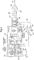
Figure 4 shows a part ofFigure 3 in greater detail. - Referring to
Figures 2 and3 , a lineariser intermediate frequency (IF) signal, which in the present embodiment can lie in the range 0 to 1GHz, online 140 is applied to the input of a divide-by-32block 102 and to the input of an IF-level flag circuit 114 whose output is fed vialine 142 to an interfacecontrol logic block 122. The output of divide-by-32block 102 is fed vialine 146 to a first input of a phases-sensitive detector (PSD) 104. Abi-directional bus 202 couples theinterface control logic 122 and a Direct Digital Synthesis (DDS)reference block 400 which will be described later with reference toFigure 4 . An
output ofDDS reference block 400 is fed vialine 144 to a second input ofPSD 104. First and second outputs from PSD 104 are fed vialines differential amplifier 106 whose output is fed vialine 152 to alock flag circuit 118 and aloop filter 108 which in the present embodiment has a cut-off frequency of 35kHz. - The filtered output signal on
line 160 is fed to a first input of asummation amplifier 110. Signals frominterface control logic 122 are fed vialine 156 to aramp generator circuit 120 whose output is fed vialine 158 to a second input ofsummation amplifier 110. The summed output is fed vialine 162 to a low-pass varactor filter 112 having a cut-off frequency fc of 350 kHz. In thepresent embodiment filter 112 is a passive Cauer filter. The output of the filter online 164 is fed to the frequency control input of a voltage-controlled oscillator 200. - Referring now to
Figure 4 ,control interface logic 208 provides an interface viabi-directional bus 202 between the interface control logic 122 (as shown inFigure 3 ) andmodulation logic 206 and, viacontrol bus 214, a 32 bit numerically controlled oscillator (NCO) 216. Themodulation logic 206 contains down counters, multiplexers and timing circuits. Operation of NCO 216 is controlled by clockedsupport logic 230. An 8-bit bus 210 conveys modulation words as four sequential 8-bit words, and abus A 212 convey signals to a 2x4 Byte register/multiplexer 218 which converts the 4x8 byte words to 32 bit (8 byte) words which are applied via a 32bit bus 220 to a first input of a 32bit adder 222. The output ofadder 222 is a 32 bit word which is fed back via 32bit bus 224 to a second input ofadder 222. Theadder 222 and feedback path 224 constitute a 32 bit phase accumulator. The 13 most significant bits of the adder output are fed via 13-bit bus 226 to a cosine look-up table (LUT) 228. The output of the look-up table (LUT) 228 is fed viabus 232 to a 12 bit Digital-to-Analogue converter (DAC) 234 which produces an analogue output signal online 236. This signal is filtered in low-pass filter 238. The filtered analogue signal is fed vialine 240 to acircuit 242 which produces a digital output at emitter-coupled logic (ECL) levels online 144. Acrystal oscillator 250 generates clock signals online 252 which are fed viarespective buffer amplifiers lines control interface logic 208,support logic bit DAC 234 respectively. - The functions of the individual blocks will be now be described.
- The modulation and
interface logic 204 produces a 23 bit-modulation word which decrements at a 2N fraction of the master clock frequency as determined byoscillator 250. Each 32 bit-word is output on 8-bit bus 210 as four sequential 8-bit words. In the present embodiment which requires a linear ramp frequency modulation waveform, a start count of Δ phase(start) is loaded at every ramp reset, resulting in a ramp FM modulation. In principle, any arbitrary waveform could be substituted for the linear ramp according to the requirement of the system. A linear ramp is used in the present embodiment because a linearly-ramping frequency characteristic is required. - The numerically controlled
oscillator 216 receives 32 bit-modulation words from themodulation logic 204 at one quarter of the master clock frequency as a consequency of the 32-bit word being conveyed in four x 8 bit sections. - The modulation word is phase-accumulated by means of the
feedback path 224 so that the 13 bit output word onbus 226 represents the real time phase of the oscillator signal to be generated. This 13 bit word is then passed to the sine/cosine look-up table to generate the 12-bit numeric oscillator signal which is a digital representation of the instantaneous amplitude of the desired oscillator output signal. The numeric oscillator signal is converted to an analogue signal inDAC 234 whose output is updated at the frequency of themaster clock 250. - The modulation word Δ phase on
bus 220 effectively directly sets the frequency of the analogue sinusoid emerging fromDAC 234 in accordance with the equation
line 236, fc is the clock frequency ofmaster clock 250, and Δ phase is the decimal value for the 32-bit modulation word onbus 220. -
DAC 234, which converts the NCO word onbus 232 to an analogue signal online 236, has the following requirements: - i low glitch energy,
- ii low spurious-free dynamic range,
- iii low differential non-linear performance, and
- iv low integral non-linear performance.
-
DAC 234 determines the Phase Modulation (PM) noise performance of the radar baseband Intermediate frequency (IF), the IF being determined from a homodyne mix of transmitted and target returned signals at the antenna. -
Filter 238, which removes all the digitally-generated alias components, is a high roll-off low-pass filter having sufficient stop-band attenuation at the alias frequency (half the master clock frequency) to reduce it to a negligible level. - The sine to
ECL converter 242 conveniently detects the zero crossing point of the filtered sinusoid online 240 and translates this into rising and falling transitions of ECL-level logic signals. The fast response time of ECL logic is conveniently used to ensure that the converter produces minimal skew, as skew translates directly into PM noise on the baseband IF frequency. - The phase frequency
sensitive detector 104 ofFigure 3 utilises a dual flip-flop NOR gate architecture known per se and is laser trimmed to ensure that the output signals online 152 exhibit zero dead time. The twooutputs line 144 and the prescaled lineariser IF signals online 146. The output formdifferential amplifier 106 is a variable mark-space signal whose DC component is proportional to the phase difference between the output frequency determined byNCO 216 and the prescaled lineariser IF signals online 146 up to a phase difference of 2Π. As is known to those skilled in the art, this type of PSD is capable of distinguishing differences in frequency and generates a dc voltage component which is a function of the frequency slip between the prescaled lineariser IF online 146 and the anti-aliased NCO signal online 144. - For small frequency slips a coarse correction is generated by the difference between respective widths of the "mark" and the "space" parts of the waveform. For large frequency differences the correction saturates to a fixed voltage (either logic "1" or logic "0" according to whether one frequency is higher or lower than the other). This gives the phase lock loop a very wide pull-in capability in conjunction with a very low PM noise capability. When the loop is phase locked, zero corrections are generated as there is zero error to correct. The lineariser IF prescaler is a divide-by-N which enables the loop to lock to a lineariser IF of Nxf0 where f0 is the NCO frequency. In the present embodiment N=32 but any other value can of course be used according to designed requirements in the usual manner.
- The
loop filter 108 ofFigure 3 is a conventional loop filter for limiting correction bandwidth and setting the damping factor of the loop for optimal noise performance. In the present embodiment it is critically damped and has a cut-off frequency of 35kHz. Thesummation amplifier 110 sums together the filtered correction signal online 160 with the offset and open loop ramp voltage online 158. Thevaractor filter 112 limits semiconductor noise and prevents higher frequency modulation of the varactor which would otherwise generate noise floor lift on baseband IF. The roll-off is about 10 times the loop bandwidth. The filter has a low in-band phase lag to ensure phase lock-up. - Having thus described the present invention by reference to a preferred embodiment, it is to be appreciated that the embodiment is in all respects exemplary and that modifications and variations are possible without departure from the scope of the invention. For example, whilst in the described embodiment a linear ramp frequency modulation waveform is used, any arbitrary waveform could be readily substituted for the linear ramp in accordance with the particular requirements of the system. Further, it is to be appreciated that various components of the above-discussed circuitry in the embodiment could be appropriately modified in accordance with design requirements of the system, if desired, whilst providing the same inventive technical effect.
Claims (7)
- A swept frequency source for an FMCW radar comprising a phase-locked loop frequency synthesiser, the phase-locked loop including:a voltage- controlled oscillator (200);means (120) for generating a first swept frequency waveform (158);means (110, 112) for modulating the voltage-controlled oscillator (200) with the first swept frequency waveform (158) added to a loop correction signal (160);a reference frequency source (400) for generating a reference frequency output; anda frequency/phase discriminator means (104) for generating an output voltage which by means of a loop filter (108) forms the loop correction signal (160) so controlling the voltage-controlled oscillator (200), the frequency/phase discriminator means having a first input (146), and a second input (144) for receiving the output from the reference frequency source (400);characterised in that the swept frequency source further comprises:an input for receiving a lineariser IF signal (140) whose frequency is in a predetermined IF relationship to the instantaneous output frequency of the voltage-controlled oscillator (200);the swept frequency source further comprising:prescaler means (102) for dividing the frequency of the lineariser IF signal (140) by a fixed number; anda means to apply the prescaled lineariser IF signal (146) to the first input (146) of the frequency/phase discriminator means.
- A swept frequency source as claimed in claim 1 in which the first swept frequency waveform comprises a linear ramp waveform arranged to generate a voltage-controlled oscillator output frequency whose frequency changes by equal increments in equal intervals of time, and in which the reference frequency source (400) is adapted to provide a linear frequency ramp by means of Direct Digital Synthesis, the reference frequency source (400) comprising:a numeric oscillator (216) to repetitively generate digital words, each digital word representing the instantaneous amplitude of the desired oscillator output signal at each respective predetermined instant of time; andmeans for loading a start count and conveying the generated digital words to the numerically controlled oscillator (216),the numeric oscillator (216) comprising:accumulator means (224) arranged to add an instantaneous digital word with the cumulative sum of at least some of the immediately-preceding words to produce a digital sum word representing a new cumulative sum to which the next instantaneous value can be added; anda cosine look-up table (228) arranged to be addressed by at least part of the digital sum word, the look-up table output (232) contributing to said reference frequency source output via a low pass filter (238).
- A swept frequency source as claimed in claim 2, wherein the low pass filter (238) comprises a high roll-off low pass filter to remove all digitally-generated alias components.
- A swept frequency source as claimed in any preceding claim further comprising means 106 to generate a dc component that is proportional to the phase difference between the prescaled linerariser IF signal (146) and the output frequency determined by the numeric oscillator (216).
- A swept frequency source as claimed in any preceding claim further comprising a loop filter (108) for limiting the correction bandwidth and setting the damping factor of the loop for optimal noise performance.
- A method of generating a swept frequency for an FMCW radar using a phase-locked loop frequency synthesiser comprising the steps of(a) providing a phase-locked loop comprising a reference frequency source (400), a frequency/phase discriminator (104) and a voltage-controlled oscillator (200);(b) modulating the voltage-controlled oscillator output frequency with a first swept frequency waveform (158);characterised in that the phase-locked loop further comprises an input (146) for a prescaled lineariser IF signal whose frequency has a predetermined IF relationship to the output frequency of the voltage-controlled oscillator (200), and the method further comprises:(c) using the prescaled lineariser IF signal and the reference frequency source output signal to produce a control signal (152) whose instantaneous amplitude represents the phase difference between the prescaled lineariser IF signal (146) and the reference frequency source output signal (144);(d) applying the control signal (152) to a loop filter (108) to provide an output signal (160); and(e) summing said output signal (160) with the first swept frequency waveform (158) to control the voltage-controlled oscillator (200).
- A method as claimed in claim 6 further comprising the steps of generating a linearly ramping voltage using sweep waveform generating means (120) in such a way as to apply a modulation signal to the frequency control input (162) of the voltage-controlled oscillator (200) via a summer component (110).
Applications Claiming Priority (3)
| Application Number | Priority Date | Filing Date | Title |
|---|---|---|---|
| GB0218166 | 2002-08-06 | ||
| GBGB0218166.7A GB0218166D0 (en) | 2002-08-06 | 2002-08-06 | Waveform lineariser |
| PCT/GB2003/003221 WO2004013969A1 (en) | 2002-08-06 | 2003-07-29 | Waveform lineariser |
Publications (2)
| Publication Number | Publication Date |
|---|---|
| EP1543622A1 EP1543622A1 (en) | 2005-06-22 |
| EP1543622B1 true EP1543622B1 (en) | 2019-01-02 |
Family
ID=9941767
Family Applications (1)
| Application Number | Title | Priority Date | Filing Date |
|---|---|---|---|
| EP03766441.4A Expired - Lifetime EP1543622B1 (en) | 2002-08-06 | 2003-07-29 | Waveform lineariser |
Country Status (6)
| Country | Link |
|---|---|
| US (1) | US7196587B2 (en) |
| EP (1) | EP1543622B1 (en) |
| AU (1) | AU2003248953A1 (en) |
| ES (1) | ES2716472T3 (en) |
| GB (1) | GB0218166D0 (en) |
| WO (1) | WO2004013969A1 (en) |
Families Citing this family (7)
| Publication number | Priority date | Publication date | Assignee | Title |
|---|---|---|---|---|
| JP2010071899A (en) * | 2008-09-19 | 2010-04-02 | Toshiba Corp | Fmcw signal generator and radar apparatus using the fmcw signal generator |
| US8098193B2 (en) * | 2009-11-05 | 2012-01-17 | Honeywell International Inc. | Digitally controlled UWB millimeter wave radar |
| US9014322B2 (en) * | 2012-05-23 | 2015-04-21 | Finisar Corporation | Low power and compact area digital integrator for a digital phase detector |
| CN105629224A (en) * | 2016-02-29 | 2016-06-01 | 珠海上富电技股份有限公司 | Frequency-modulated continuous-wave radar high-precision distance measuring method |
| CN107222171A (en) * | 2017-05-19 | 2017-09-29 | 四川莱源科技有限公司 | One kind is used for two-way swept-frequency signal speedy carding process two-way Sweep Source |
| US12265148B2 (en) * | 2019-03-25 | 2025-04-01 | Mitsubishi Electric Corporation | Radar device |
| WO2021165459A1 (en) * | 2020-02-20 | 2021-08-26 | 2Pi-Labs Gmbh | Reference oscillator arrangement, radar system and method of synchronisation |
Family Cites Families (11)
| Publication number | Priority date | Publication date | Assignee | Title |
|---|---|---|---|---|
| GB1374638A (en) | 1972-06-22 | 1974-11-20 | Marconi Instruments Ltd | Oscillation generators |
| DE2914814A1 (en) | 1979-04-11 | 1980-10-30 | Siemens Ag | FREQUENCY MODULATOR |
| US5374903A (en) | 1988-04-22 | 1994-12-20 | Hughes Aircraft Company | Generation of wideband linear frequency modulation signals |
| US4998217A (en) | 1989-05-01 | 1991-03-05 | Motorola, Inc. | Sweep generator linearization system and method |
| GB2236026A (en) | 1989-09-13 | 1991-03-20 | Marconi Instruments Ltd | Swept frequency signal generating circuit |
| GB2237157A (en) | 1989-10-20 | 1991-04-24 | Marconi Instruments Ltd | Control of frequency modulators |
| GB2246042A (en) | 1990-07-11 | 1992-01-15 | Philips Electronic Associated | Fmcw radar linearizer. |
| US5130670A (en) | 1991-08-01 | 1992-07-14 | Hewlett-Packard Company | Phase-locking circuit for swept synthesized source preferably having stability enhancement circuit |
| US5642081A (en) | 1995-10-26 | 1997-06-24 | Alliant Techsystems Inc. | FMCW VCO closed loop linearizer |
| US5983077A (en) | 1997-07-31 | 1999-11-09 | Ericsson Inc. | Systems and methods for automatic deviation setting and control in radio transmitters |
| US6091356A (en) * | 1998-10-05 | 2000-07-18 | Sensor Concepts Incorporated | Chirp source with rolling frequency lock for generating linear frequency chirps |
-
2002
- 2002-08-06 GB GBGB0218166.7A patent/GB0218166D0/en not_active Ceased
-
2003
- 2003-07-29 EP EP03766441.4A patent/EP1543622B1/en not_active Expired - Lifetime
- 2003-07-29 AU AU2003248953A patent/AU2003248953A1/en not_active Abandoned
- 2003-07-29 WO PCT/GB2003/003221 patent/WO2004013969A1/en not_active Ceased
- 2003-07-29 ES ES03766441T patent/ES2716472T3/en not_active Expired - Lifetime
- 2003-07-29 US US10/523,713 patent/US7196587B2/en not_active Expired - Lifetime
Non-Patent Citations (1)
| Title |
|---|
| None * |
Also Published As
| Publication number | Publication date |
|---|---|
| US7196587B2 (en) | 2007-03-27 |
| ES2716472T3 (en) | 2019-06-12 |
| WO2004013969A1 (en) | 2004-02-12 |
| GB0218166D0 (en) | 2002-09-11 |
| EP1543622A1 (en) | 2005-06-22 |
| AU2003248953A1 (en) | 2004-02-23 |
| US20060164173A1 (en) | 2006-07-27 |
Similar Documents
| Publication | Publication Date | Title |
|---|---|---|
| US5604468A (en) | Frequency synthesizer with temperature compensation and frequency multiplication and method of providing the same | |
| EP1330035B1 (en) | Fractional-N frequency synthesizer with sine wave generator | |
| EP0479969B1 (en) | Fractional-division synthesizer for a voice/data communications system | |
| KR0153180B1 (en) | Fractional N frequency synthesizer and frequency synthesis method | |
| JP2650492B2 (en) | Fractional-N synthesizer with modulation spurious compensation | |
| US7567099B2 (en) | Filterless digital frequency locked loop | |
| AU658097B2 (en) | High spectral purity digital waveform synthesiser | |
| EP1434352B1 (en) | Delay-compensated fractional-N frequency synthesizer | |
| US20020136341A1 (en) | Fractional-N frequency synthesizer with fractional compensation method | |
| JPS61245629A (en) | N fraction type frequency synthesizer | |
| WO1999000902A1 (en) | Communication device a frequency compensating synthesizer and method of providing same | |
| EP3700091B1 (en) | Feedback control for accurate signal generation | |
| EP2369745B1 (en) | Method and apparatus for quantization noise reduction in fractional-N PLLS | |
| US11804847B2 (en) | Fractional frequency synthesis by sigma-delta modulating frequency of a reference clock | |
| US9571071B2 (en) | Frequency synthesizer circuit | |
| US7327820B2 (en) | Method and apparatus for reducing quantization noise in fractional-N frequency synthesizers | |
| US6697416B1 (en) | Digital programmable, spread spectrum clock generator | |
| JP4903969B2 (en) | Rotational frequency synthesizer | |
| US6943598B2 (en) | Reduced-size integrated phase-locked loop | |
| KR101581528B1 (en) | Synthesizing Method of Signal having Variable Frequency and Synthesizer of Signal having Variable Frequency | |
| US7196587B2 (en) | Waveform lineariser | |
| US7298790B2 (en) | Low frequency self-calibration of a PLL with multiphase clocks | |
| US20050036580A1 (en) | Programmable phase-locked loop fractional-N frequency synthesizer | |
| Kameche et al. | Designing and simulating a 2.4 ghz integer-n frequency synthesizer with 1 mhz frequency step | |
| JPH10224218A (en) | Signal generator |
Legal Events
| Date | Code | Title | Description |
|---|---|---|---|
| PUAI | Public reference made under article 153(3) epc to a published international application that has entered the european phase |
Free format text: ORIGINAL CODE: 0009012 |
|
| 17P | Request for examination filed |
Effective date: 20050221 |
|
| AK | Designated contracting states |
Kind code of ref document: A1 Designated state(s): AT BE BG CH CY CZ DE DK EE ES FI FR GB GR HU IE IT LI LU MC NL PT RO SE SI SK TR |
|
| AX | Request for extension of the european patent |
Extension state: AL LT LV MK |
|
| DAX | Request for extension of the european patent (deleted) | ||
| GRAP | Despatch of communication of intention to grant a patent |
Free format text: ORIGINAL CODE: EPIDOSNIGR1 |
|
| STAA | Information on the status of an ep patent application or granted ep patent |
Free format text: STATUS: GRANT OF PATENT IS INTENDED |
|
| INTG | Intention to grant announced |
Effective date: 20180509 |
|
| GRAJ | Information related to disapproval of communication of intention to grant by the applicant or resumption of examination proceedings by the epo deleted |
Free format text: ORIGINAL CODE: EPIDOSDIGR1 |
|
| STAA | Information on the status of an ep patent application or granted ep patent |
Free format text: STATUS: EXAMINATION IS IN PROGRESS |
|
| INTC | Intention to grant announced (deleted) | ||
| GRAP | Despatch of communication of intention to grant a patent |
Free format text: ORIGINAL CODE: EPIDOSNIGR1 |
|
| STAA | Information on the status of an ep patent application or granted ep patent |
Free format text: STATUS: GRANT OF PATENT IS INTENDED |
|
| INTG | Intention to grant announced |
Effective date: 20180830 |
|
| GRAS | Grant fee paid |
Free format text: ORIGINAL CODE: EPIDOSNIGR3 |
|
| GRAA | (expected) grant |
Free format text: ORIGINAL CODE: 0009210 |
|
| STAA | Information on the status of an ep patent application or granted ep patent |
Free format text: STATUS: THE PATENT HAS BEEN GRANTED |
|
| AK | Designated contracting states |
Kind code of ref document: B1 Designated state(s): AT BE BG CH CY CZ DE DK EE ES FI FR GB GR HU IE IT LI LU MC NL PT RO SE SI SK TR |
|
| REG | Reference to a national code |
Ref country code: GB Ref legal event code: FG4D |
|
| REG | Reference to a national code |
Ref country code: CH Ref legal event code: EP Ref country code: AT Ref legal event code: REF Ref document number: 1085718 Country of ref document: AT Kind code of ref document: T Effective date: 20190115 |
|
| REG | Reference to a national code |
Ref country code: IE Ref legal event code: FG4D |
|
| REG | Reference to a national code |
Ref country code: DE Ref legal event code: R096 Ref document number: 60351746 Country of ref document: DE Ref country code: CH Ref legal event code: PK Free format text: BERICHTIGUNGEN |
|
| RIC2 | Information provided on ipc code assigned after grant |
Ipc: H03L 7/18 20060101AFI20040225BHEP Ipc: G01S 7/40 20060101ALI20040225BHEP |
|
| REG | Reference to a national code |
Ref country code: SE Ref legal event code: TRGR |
|
| REG | Reference to a national code |
Ref country code: NL Ref legal event code: MP Effective date: 20190102 |
|
| REG | Reference to a national code |
Ref country code: ES Ref legal event code: FG2A Ref document number: 2716472 Country of ref document: ES Kind code of ref document: T3 Effective date: 20190612 |
|
| REG | Reference to a national code |
Ref country code: AT Ref legal event code: MK05 Ref document number: 1085718 Country of ref document: AT Kind code of ref document: T Effective date: 20190102 |
|
| PG25 | Lapsed in a contracting state [announced via postgrant information from national office to epo] |
Ref country code: NL Free format text: LAPSE BECAUSE OF FAILURE TO SUBMIT A TRANSLATION OF THE DESCRIPTION OR TO PAY THE FEE WITHIN THE PRESCRIBED TIME-LIMIT Effective date: 20190102 |
|
| PG25 | Lapsed in a contracting state [announced via postgrant information from national office to epo] |
Ref country code: PT Free format text: LAPSE BECAUSE OF FAILURE TO SUBMIT A TRANSLATION OF THE DESCRIPTION OR TO PAY THE FEE WITHIN THE PRESCRIBED TIME-LIMIT Effective date: 20190502 |
|
| PG25 | Lapsed in a contracting state [announced via postgrant information from national office to epo] |
Ref country code: GR Free format text: LAPSE BECAUSE OF FAILURE TO SUBMIT A TRANSLATION OF THE DESCRIPTION OR TO PAY THE FEE WITHIN THE PRESCRIBED TIME-LIMIT Effective date: 20190403 Ref country code: BG Free format text: LAPSE BECAUSE OF FAILURE TO SUBMIT A TRANSLATION OF THE DESCRIPTION OR TO PAY THE FEE WITHIN THE PRESCRIBED TIME-LIMIT Effective date: 20190402 |
|
| REG | Reference to a national code |
Ref country code: DE Ref legal event code: R097 Ref document number: 60351746 Country of ref document: DE |
|
| PG25 | Lapsed in a contracting state [announced via postgrant information from national office to epo] |
Ref country code: EE Free format text: LAPSE BECAUSE OF FAILURE TO SUBMIT A TRANSLATION OF THE DESCRIPTION OR TO PAY THE FEE WITHIN THE PRESCRIBED TIME-LIMIT Effective date: 20190102 Ref country code: DK Free format text: LAPSE BECAUSE OF FAILURE TO SUBMIT A TRANSLATION OF THE DESCRIPTION OR TO PAY THE FEE WITHIN THE PRESCRIBED TIME-LIMIT Effective date: 20190102 Ref country code: SK Free format text: LAPSE BECAUSE OF FAILURE TO SUBMIT A TRANSLATION OF THE DESCRIPTION OR TO PAY THE FEE WITHIN THE PRESCRIBED TIME-LIMIT Effective date: 20190102 Ref country code: CZ Free format text: LAPSE BECAUSE OF FAILURE TO SUBMIT A TRANSLATION OF THE DESCRIPTION OR TO PAY THE FEE WITHIN THE PRESCRIBED TIME-LIMIT Effective date: 20190102 Ref country code: AT Free format text: LAPSE BECAUSE OF FAILURE TO SUBMIT A TRANSLATION OF THE DESCRIPTION OR TO PAY THE FEE WITHIN THE PRESCRIBED TIME-LIMIT Effective date: 20190102 Ref country code: RO Free format text: LAPSE BECAUSE OF FAILURE TO SUBMIT A TRANSLATION OF THE DESCRIPTION OR TO PAY THE FEE WITHIN THE PRESCRIBED TIME-LIMIT Effective date: 20190102 |
|
| PLBE | No opposition filed within time limit |
Free format text: ORIGINAL CODE: 0009261 |
|
| STAA | Information on the status of an ep patent application or granted ep patent |
Free format text: STATUS: NO OPPOSITION FILED WITHIN TIME LIMIT |
|
| 26N | No opposition filed |
Effective date: 20191003 |
|
| PG25 | Lapsed in a contracting state [announced via postgrant information from national office to epo] |
Ref country code: MC Free format text: LAPSE BECAUSE OF FAILURE TO SUBMIT A TRANSLATION OF THE DESCRIPTION OR TO PAY THE FEE WITHIN THE PRESCRIBED TIME-LIMIT Effective date: 20190102 Ref country code: SI Free format text: LAPSE BECAUSE OF FAILURE TO SUBMIT A TRANSLATION OF THE DESCRIPTION OR TO PAY THE FEE WITHIN THE PRESCRIBED TIME-LIMIT Effective date: 20190102 |
|
| REG | Reference to a national code |
Ref country code: CH Ref legal event code: PL |
|
| PG25 | Lapsed in a contracting state [announced via postgrant information from national office to epo] |
Ref country code: TR Free format text: LAPSE BECAUSE OF FAILURE TO SUBMIT A TRANSLATION OF THE DESCRIPTION OR TO PAY THE FEE WITHIN THE PRESCRIBED TIME-LIMIT Effective date: 20190102 |
|
| REG | Reference to a national code |
Ref country code: BE Ref legal event code: MM Effective date: 20190731 |
|
| PG25 | Lapsed in a contracting state [announced via postgrant information from national office to epo] |
Ref country code: LI Free format text: LAPSE BECAUSE OF NON-PAYMENT OF DUE FEES Effective date: 20190731 Ref country code: CH Free format text: LAPSE BECAUSE OF NON-PAYMENT OF DUE FEES Effective date: 20190731 Ref country code: LU Free format text: LAPSE BECAUSE OF NON-PAYMENT OF DUE FEES Effective date: 20190729 Ref country code: BE Free format text: LAPSE BECAUSE OF NON-PAYMENT OF DUE FEES Effective date: 20190731 |
|
| PG25 | Lapsed in a contracting state [announced via postgrant information from national office to epo] |
Ref country code: IE Free format text: LAPSE BECAUSE OF NON-PAYMENT OF DUE FEES Effective date: 20190729 |
|
| PG25 | Lapsed in a contracting state [announced via postgrant information from national office to epo] |
Ref country code: CY Free format text: LAPSE BECAUSE OF FAILURE TO SUBMIT A TRANSLATION OF THE DESCRIPTION OR TO PAY THE FEE WITHIN THE PRESCRIBED TIME-LIMIT Effective date: 20190102 |
|
| PG25 | Lapsed in a contracting state [announced via postgrant information from national office to epo] |
Ref country code: HU Free format text: LAPSE BECAUSE OF FAILURE TO SUBMIT A TRANSLATION OF THE DESCRIPTION OR TO PAY THE FEE WITHIN THE PRESCRIBED TIME-LIMIT; INVALID AB INITIO Effective date: 20030729 |
|
| PGFP | Annual fee paid to national office [announced via postgrant information from national office to epo] |
Ref country code: SE Payment date: 20220722 Year of fee payment: 20 Ref country code: IT Payment date: 20220725 Year of fee payment: 20 Ref country code: GB Payment date: 20220719 Year of fee payment: 20 Ref country code: FI Payment date: 20220719 Year of fee payment: 20 Ref country code: ES Payment date: 20220817 Year of fee payment: 20 Ref country code: DE Payment date: 20220727 Year of fee payment: 20 |
|
| PGFP | Annual fee paid to national office [announced via postgrant information from national office to epo] |
Ref country code: FR Payment date: 20220725 Year of fee payment: 20 |
|
| REG | Reference to a national code |
Ref country code: DE Ref legal event code: R071 Ref document number: 60351746 Country of ref document: DE |
|
| REG | Reference to a national code |
Ref country code: ES Ref legal event code: FD2A Effective date: 20230804 |
|
| REG | Reference to a national code |
Ref country code: GB Ref legal event code: PE20 Expiry date: 20230728 |
|
| REG | Reference to a national code |
Ref country code: SE Ref legal event code: EUG |
|
| PG25 | Lapsed in a contracting state [announced via postgrant information from national office to epo] |
Ref country code: GB Free format text: LAPSE BECAUSE OF EXPIRATION OF PROTECTION Effective date: 20230728 Ref country code: ES Free format text: LAPSE BECAUSE OF EXPIRATION OF PROTECTION Effective date: 20230730 |