EP1542202A2 - Device and method for display control, and the like - Google Patents
Device and method for display control, and the like Download PDFInfo
- Publication number
- EP1542202A2 EP1542202A2 EP04029056A EP04029056A EP1542202A2 EP 1542202 A2 EP1542202 A2 EP 1542202A2 EP 04029056 A EP04029056 A EP 04029056A EP 04029056 A EP04029056 A EP 04029056A EP 1542202 A2 EP1542202 A2 EP 1542202A2
- Authority
- EP
- European Patent Office
- Prior art keywords
- display
- signal
- timing
- adjustment signal
- display adjustment
- Prior art date
- Legal status (The legal status is an assumption and is not a legal conclusion. Google has not performed a legal analysis and makes no representation as to the accuracy of the status listed.)
- Withdrawn
Links
Images







Classifications
-
- G—PHYSICS
- G09—EDUCATION; CRYPTOGRAPHY; DISPLAY; ADVERTISING; SEALS
- G09G—ARRANGEMENTS OR CIRCUITS FOR CONTROL OF INDICATING DEVICES USING STATIC MEANS TO PRESENT VARIABLE INFORMATION
- G09G5/00—Control arrangements or circuits for visual indicators common to cathode-ray tube indicators and other visual indicators
- G09G5/003—Details of a display terminal, the details relating to the control arrangement of the display terminal and to the interfaces thereto
- G09G5/006—Details of the interface to the display terminal
-
- G—PHYSICS
- G09—EDUCATION; CRYPTOGRAPHY; DISPLAY; ADVERTISING; SEALS
- G09G—ARRANGEMENTS OR CIRCUITS FOR CONTROL OF INDICATING DEVICES USING STATIC MEANS TO PRESENT VARIABLE INFORMATION
- G09G5/00—Control arrangements or circuits for visual indicators common to cathode-ray tube indicators and other visual indicators
- G09G5/003—Details of a display terminal, the details relating to the control arrangement of the display terminal and to the interfaces thereto
- G09G5/005—Adapting incoming signals to the display format of the display terminal
-
- G—PHYSICS
- G09—EDUCATION; CRYPTOGRAPHY; DISPLAY; ADVERTISING; SEALS
- G09G—ARRANGEMENTS OR CIRCUITS FOR CONTROL OF INDICATING DEVICES USING STATIC MEANS TO PRESENT VARIABLE INFORMATION
- G09G5/00—Control arrangements or circuits for visual indicators common to cathode-ray tube indicators and other visual indicators
- G09G5/18—Timing circuits for raster scan displays
Definitions
- the invention relates to the technical field of a display control device and method, and the like which permit a display screen to display predetermined image information.
- a display part such as a monitor or a display has displayed an image (or a picture) with higher definition.
- the approach of making the number of display pixels of the display part equal to the number of pixels of an image signal having image information is adopted as one approach for making full use of display capabilities of the display part.
- a navigation system includes a graphics part which outputs an image signal having map image information in accordance with the number of display pixels of the display part so that the number of pixels of the image signal is equal to the number of display pixels of the display part, whereby the navigation system provides a clear (or sharp) image (or picture).
- Japanese Paten Application Laid-Open No. 2000-122621 discloses a display device capable of matching the timing of display of each pixel on a display part to a display clock signal for regulating the timing of display of each pixel, thereby preventing an image from bleeding or becoming blurred.
- the display device includes a picture generator which outputs a picture signal, in which a fine horizontal adjustment signal for regulating the timing of display of each pixel of a display picture is superimposed on a predetermined horizontal scanning line within a vertical retrace interval corresponding to an out-of-frame region which lies outside a display screen of the display part and does not contribute to the display picture.
- a comparison is made between a reference voltage and a portion at or near the peak value of the fine horizontal adjustment signal (e.g., a non-square wave),that is, a threshold is taken.
- the signal is subj ected to waveform shaping, and the resulting signal is outputted to act as a HIGH signal.
- the timing of the display clock signal is adjusted in accordance with the timing of the HIGH signal.
- the above-mentioned conventional display device has the problemof failing to detect the fine horizontal adj ustment signal when the signal does not go above a threshold level due to a decrease in signal-level or the like, because the display device is designed to take a threshold for detecting a portion at or near the peak value of the fine horizontal adj ustment signal.
- a low threshold level leads to the problem of causing a time lag in the peak value of the fine horizontal adjustment signal and thus causing a time lag in the timing of display of each pixel.
- the fine horizontal adjustment signal for superimposition is not under strict control, the following problem arises: there is a time lag relative to the threshold level, and thus there is a time lag in the timing of display of each pixel.
- the invention of claim 22 relates to a display control method which permits a display screen to display predetermined image information, comprising:
- the invention of claim 23 relates to a recording medium which records a computer-readable display control program which runs on a computer which permits a display screen to display predetermined image information, the display control program which permits the computer to execute a display control method comprising:
- FIG. 1 the description is given with reference to FIG. 1 and other drawings with regard to the configuration and functions of a display control device included in a car navigation system according to a first embodiment of the invention.
- a display control device SX1 includes a graphics part 1 which acts as an example of a display adj ustment signal superimposing device, an image (or picture) processor 2, a detection/decision part 3 which acts as an example of a detecting device, a display controller 4 having a timing adjustment part 4a which acts as an example of an adjusting device, and a display part 5 such as a liquid crystal display.
- the graphics part 1 generates a signal for displaying image (or picture) information (i.e., image information to be displayed on a display screen of the display part 5) containing map information under the command of the controller of the car navigation system, such as an image (or picture) signal corresponding to each of RGB color components.
- image (or picture) information i.e., image information to be displayed on a display screen of the display part 5
- map information under the command of the controller of the car navigation system, such as an image (or picture) signal corresponding to each of RGB color components.
- the graphics part 1 superimposes a display adjustment signal (e.g., a square-wave signal) for adjusting the timing of display of each pixel of the image information upon, for example, the R-component image signal on a horizontal scanning line in a signal portion which corresponds to a region outside the display screen of the display part 5 and also corresponds to a region capable of displaying the image information.
- a display adjustment signal e.g., a square-wave signal
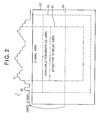
- the available-for-graphics area 52 is the region capable of displaying image information. Specifically, a region lying both outside the effective display area 51 and inside the available-for-graphics area 52 does not display image information, because the actual display screen region lies within the effective display area 51. However, the display part 5 having a larger display screen region enables the available-for-graphics area 52 to display image information. In other words, the region lying both outside the effective display area 51 and inside the available-for-graphics area 52 corresponds to the region outside the display screen and also corresponds to the region capable of displaying image information.
- a region lying both outside the available-for-graphics area 52 and inside the signal area 53 is the region which does not contribute to a display image (i.e., the region incapable of displaying image information).
- each pixel signal 61 and the display adjustment signal 62 have so-called rounding having a gradual rising edge. This results from, for example, the influence of the length of a transmission line (e.g., in the car navigation system, a cable between the graphics part 1 and the image processor 2 or between the image processor 2 and the detection/decision part 3 may be as long as 1 to 6 m) , the influence of frequency characteristics of the transmission line, or the like.
- a transmission line e.g., in the car navigation system, a cable between the graphics part 1 and the image processor 2 or between the image processor 2 and the detection/decision part 3 may be as long as 1 to 6 m
- the influence of frequency characteristics of the transmission line or the like.
- the image signal generated as mentioned above is outputted in conjunction with a synchronization signal to the image processor 2.
- the graphics part 1 can superimpose the display adjustment signal 62 on the image signal in the signal portion corresponding to the region lying both outside the effective display area 51 and inside the available-for-graphics area 52.
- the display controller 4 Upon receipt of the image signal, the horizontal and vertical synchronization signals, and other signals from the image processor 2 and the detection/decision part 3, the display controller 4 then outputs these input signals to the display part 5. Moreover, the timing adjustment part 4a adjusts the phase of the clock signal in accordance with the clock phase adjustment signal from the detection/decision part 3 in order to bring the clock signal into synchronization with the timing of each pixel signal 61 having the maximum value (step S5). The display controller 4 outputs the clock signal to the display part 5.
- the display part 5 receives the clock signal in synchronization with the timing of each pixel signal 61, of the image information contained in the image signal, having the maximum value.
- the horizontal and vertical drivers drive the pixels on each line on the liquid crystal panel in synchronization with the clock signal.
- the display screen of the liquid crystal panel displays clear image information.
- FIGs. 5A to 5D are conceptual illustrations showing an example of the relation between the phases of the image signal and the clock signal for use in the example 1.
- FIG. 5A shows each pixel signal 61 and the display adjustment signal 62 which appear immediately after being outputted by the graphics part 1.
- FIG. 5B shows each pixel signal 61 and the display adjustment signal 62 which appear immediately before being inputted to the display controller 4.
- FIG. 5C shows the clock signal which appears before the timing adjustment part 4a subjects the clock signal to phase adjustment.
- FIG. 5D shows the clock signal which appears after the timing adjustment part 4a subjects the clock signal to phase adjustment.
- each pixel signal 61 and the display adjustment signal 62 do not have rounding or the like, but have respective flat peaks, as shown in FIG. 5A.
- each pixel signal 61 and the display adjustment signal 62 are rounded and delayed under the influence of, for example, the length of the transmission line, the frequency characteristics of the transmission line, or the like, as shown in FIG. 5B.
- a center point T of the display adjustment signal 62 shown in FIG. 5A is a reference point of the display adjustment signal 62
- a phase difference (or shift) between the reference point T and a maximum point M of the display adjustment signal 62 shown in FIG. 58 is equivalent to ⁇ T.
- ⁇ T the same holds true for each pixel signal 61.
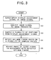
- the display control device SX1 of the above-mentioned example 1 is configured to perform the processing which includes the steps of: sampling a plurality of portions from the display adjustment signal superimposed on the image signal; detecting the timing of the display adjustment signal having the maximum or minimum value of a plurality of sampled values, thereby detecting the optimum timing; and adjusting the timing of display of each pixel of the image information in accordance with the detected optimum timing.
- the display control device SX1 enables a more exact match between the timing of output of the image signal from the graphic part 1 and the timing of display of each pixel on the display part, and thus enables displaying a clearer image, even when the image signal is delayed or is rounded or otherwise distorted under the influence of, for example, the length of the transmission line, the frequency characteristics of the transmission line, or the like. Moreover, the display control device SX1 allows sampling a plurality of portions from a 1-pulse display adjustment signal in synchronization with a graphic dot, and thus enables detecting the optimum timing with greater precision.
- the detection/decision part 3 detects the optimum timing by detecting the timing of the display adj ustment signal having the maximum or minimum value of a plurality of sampled values.
- the detection/decision part 3 detects the optimum timing through the procedure which involves detecting the timing of the display adjustment signal having the maximum or minimum value, and detecting the timing at which the display adjustment signal is shifted in phase from the detected timing by a predefined amount of offset.
- the timing at which the display adjustment signal is shifted in phase by the amount of offset is used as the optimum timing as mentioned above, because it may be inappropriate to use as the optimum timing the detected timing of the display adjustment signal having the maximum or minimum value, for example in the following situations: (i) where an image signal is delayed between the display controller 4 and the display part 5; (ii) where an image signal is delayed when the image signal is temporarily stored in a memory or the like in the display part 5 or the like; and (iii) where the display controller 4 has the amount of jitter near an adjacent pixel at the timing of the display adjustment signal having the maximum or minimum value.
- the amount of offset is set to the optimum value according to the device in consideration of the above situations (i) to (iii) and others.
- the amount of offset may be set to a positive or negative value.
- FIGs. 5A to 5D The processing shown in FIGs. 5A to 5D is applied to processing which the display control device SX1 of the example 2 performs. Since steps S1 to S3 shown in FIG. 3 take place as in the case of the example 1, the repeated description of these steps is omitted.
- the detection/decision part 3 detects the optimum timing through the procedure which involves detecting the timing of the display adjustment signal having the maximum (or minimum) value of a plurality of sampled values, and detecting the timing at which the display adjustment signal is shifted in phase from the detected timing by a predefined amount of offset.
- the detection/decision part 3 outputs to the display controller 4 the dot clock phase adjustment signal indicative of the detected optimum timing.
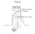
- FIG. 6 is an illustration showing an example of the sampling timing and the optimum timing of the display adjustment signal for use in the example 2.
- timing GX shifted by the amount of offset from the timing of the display adjustment signal having the maximum value "G" of five sampled values is detected for detection of the optimum timing.
- the sampling interval may be fixed or appropriately settable by the operating part or the like.
- step S5 upon receipt of the image signal and the horizontal and vertical synchronization signals from the image processor 2 and the detection/decision part 3, the display controller 4 then outputs these input signals to the display part 5. Moreover, the timing adjustment part 4a adjusts the phase of the clock signal in accordance with the clock phase adjustment signal from the detection/decision part 3 in order to bring the clock signal into synchronization with the timing shifted by the amount of offset from the timing of each pixel signal 61 having the maximum value. The display controller 4 outputs the clock signal to the display part 5.
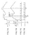
- FIGs. 7A to 7D are conceptual illustrations showing an example of the relation between the phases of the image signal and the clock signal for use in the example 2.
- FIG. 7A shows the image signal (i.e., each pixel signal 61a and a display adjustment signal 62a) which appears immediately after being outputted by the graphics part 1, similarly to FIG. 5A.
- FIG. 7B shows the image signal (i.e., each pixel signal 61a and the display adjustment signal 62a) which appears immediately before being inputted to the display controller 4, similarly to FIG. 5B.
- FIG. 7C shows the clock signal which appears before the timing adjustment part 4a subjects the clock signal to phase adjustment, similarly to FIG. 5C.
- FIG. 7D shows the clock signal which appears after the timing adjustment part 4a subjects the clock signal to phase adjustment, similarly to FIG. 5D.
- the unadjusted clock signal shown in FIG. 7C is changed into the clock signal shown in FIG. 7D through adjustment which involves shifting the phase of the unadjusted clock signal by a phase difference ⁇ T between the reference point T and an optimum point MX shifted by the amount ⁇ T1 of offset from the maximum point M of the display adjustment signal 62a shown in FIG. 7B.
- the display control device SX1 of the above-mentioned example 2 is configured to perform the processing which includes the steps of: sampling a plurality of portions from the display adjustment signal superimposed on the image signal; detecting the timing of the display adjustment signal having the maximum or minimum value of a plurality of sampled values, and detecting the timing at which the display adjustment signal is shifted in phase from the detected timing by a predefined amount of offset, thereby detecting the optimum timing; and adjusting the timing of display of each pixel of the image information in accordance with the detected optimum timing.
- the display control device SX1 of the example 2 enables a more exact match between the timing of output of the image signal from the graphics part 1 and the timing of display of each pixel on the display part, and thus enables displaying a clearer image, even when the image signal is delayed or is rounded or otherwise distorted under the influence of, for example, the length of the transmission line, the frequency characteristics of the transmission line, or the like, and moreover when it is not appropriate to use as the optimum timing the timing of the display adjustment signal having the maximum or minimum value under the influence of the above situations (i) to (iii) and so on (e.g., when an adjacent pixel is subjected to display sampling using the clock signal when the display controller 4 has the amount of jitter as mentioned above).
- the detection/decision part 3 samples a plurality of portions from a 1-pulse signal which is the display adjustment signal, and detects the optimum timing based on a plurality of sampled values.
- the detection/decision part 3 samples respective portions of a plurality of pulses from a multi-pulse signal, and detects the optimum timing based on a plurality of sampled values.
- the processing shown in FIG. 3 is applied to processing which the display control device SX1 of the example 3 performs.
- the detection/decision part 3 may be configured to detect the optimum timing through the procedure which involves detecting the timing of the display adjustment signal having the maximum or minimum value of a plurality of sampled values, and detecting the timing at which the display adj ustment signal is shifted in phase fromthe detected timing by a predefined amount of offset.
- FIG. 8 is an illustration showing an example of the sampling timing and the optimum timing of the display adjustment signal for use in the example 3.
- a display adjustment signal 62b having no rounding.
- the display adjustment signal 62b actually has rounding in the same manner as the display adjustment signals shown in FIG. 4 and other drawings.
- one portion, in each High-level interval, of the display adjustment signal 62b having five repetitions of HIGH and LOW levels is used as a sampling point.
- the sampling timing for each High-level interval is shifted by a predetermined interval.
- the sampling timing G for the fourth HIGH-level is detected for detection of the timing of the display adjustment signal 62b having the maximum value.
- the display control device SX1 of the above-mentioned example 3 is configured to perform the processing which includes: the step of sampling at least one portion from each of a plurality of display adjustment signals while shifting the sampling timing (i.e., long-interval sampling) , rather than the sampling step of the examples 1 and 2, specifically the step of sampling a plurality of portions from the display adjustment signal corresponding to one display pixel (i.e., short-interval sampling); the step of detecting the optimum timing based on a plurality of sampled values; and the step of adjusting the timing of display of each pixel of the image information in accordance with the detected optimum timing.
- the processing which includes: the step of sampling at least one portion from each of a plurality of display adjustment signals while shifting the sampling timing (i.e., long-interval sampling) , rather than the sampling step of the examples 1 and 2, specifically the step of sampling a plurality of portions from the display adjustment signal corresponding to one display pixel (i.e., short-interval sampling); the step of
- the detection/decision part 3 first detects the timing of the display adjustment signal having the maximum or minimum value of a plurality of sampled values, and then detects the optimum timing based on the detected timing.
- the detection/decision part 3 samples aportionfromthe display adjustment signal in each of High-level and Low-level intervals having the same interval, then calculates the differential value between the sampled value in the High-level interval and the sampled value in the Low-level interval, and then detects the optimum timing by detecting the timing of the display adjustment signal having the maximum value of a plurality of calculated differential values.
- the graphics part 1 superimposes a plurality of 1-pulse display adjustment signals, one of which is used in the examples 1 and 2, (specifically, this signal is the signal in synchronization with a graphic dot, such as the signal corresponding to one display pixel, as in the case of the examples 1 and 2).
- step S2 takes place as in the case of the example 1.
- the detection/decision part 3 upon receipt of the image signal from the image processor 2, the detection/decision part 3 outputs the input image signal to the display controller 4.
- the detection/decision part 3 performs sampling for each of a plurality of sets of HIGH and LOW levels (i.e., a set of HIGH and LOW levels) so as to sample at least one portion in a High-level interval and a portion distant from the one portion by a given (or preset) interval in a Low-level interval following the High-level interval.
- the detection/decision part 3 performs sampling, while shifting the sampling timing for each set by a predetermined interval (e.g., the sampling interval for use in the example 1, shown in FIG. 4).
- step S4 the detection/decision part 3 calculates the differential value between the sampled values in the High-level and Low-level intervals of each set, and detects the optimum timing by detecting the timing of the display adjustment signal having the maximum value (i.e., maximum contrast) of a plurality of calculated differential values.
- the detection/decision part 3 outputs to the display controller 4 the dot clock phase adjustment signal indicative of the detected optimum timing.
- the detection/decision part 3 may be configured to detect the optimum timing through the procedure which involves detecting the timing of the display adjustment signal having the maximum value of a plurality of calculated differential values, and detecting the timing at which thedisplayadjustment signal is shiftedinphase fromthedetected timing by a predefined amount of offset.
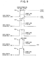
- FIG. 10 is an illustration showing an example of the sampling timing and the optimum timing of the display adjustment signal for use in the example 4.
- a display adjustment signal 62d having no rounding.
- the display adjustment signal 62d actually has rounding in the same manner as the display adjustment signals shown in FIG. 4 and other drawings.
- the portion distant by the given interval is the point distant by an interval which is equal to the interval between the sampling point in the High-level interval and the dropping edge of the pulse plus the predetermined interval.
- the sampling timing for each set is shifted by a predetermined interval.
- the optimum timing is the timing G
- the differential value between the sampled values in the High-level and Low-level intervals of the fourth set is the maximum value (i.e., maximum contrast).
- step S5 of the example 4 is the same as that of the example 1 or 2, the repeated description of this step is omitted.
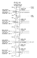
- the detection/decision part 3 performs sampling, while shifting the sampling timing for two horizontal scanning lines each by a predetermined interval ⁇ TS.
- the detection/decision part 3 performs a plurality of sequential calculations of the sampled value of the display adjustment signal and the differential value between the display adjustment signal and a next display adjustment signal having an inverted signal-level.
- the detection/decision part 3 detects the optimum timing by detecting the timing of the display adjustment signal having the maximum value (i.e., maximum contrast) of a plurality of calculated differential values.
- the sampling interval ⁇ TS may be fixed or appropriately settable by the operating part or the like.
- FIG. 11 is an illustration showing another example of the sampling timing and the optimum timing of the display adjustment signal for use in the example 4.
- a display adjustment signal 62e having no rounding.
- the display adjustment signal 62e actually has rounding in the same manner as the display adjustment signals shown in FIG. 4 and other drawings.
- the display control device SX1 of the above-mentioned example 4 is configured to perform the processing which includes: the step of detecting the optimum timing based on the timing of the maximum differential value between the sampled values, rather than the step of detecting the optimum timing based on the timing of the maximum or minimum value of the sampled values of the display adjustment signal; and the step of adjusting the timing of display of each pixel of the image information in accordance with the detected optimum timing. Therefore, the display control device SX1 of the example 4 enables a match between the timing of the maximum contrast and the timing of display of each pixel and thus enables displaying a clearer image, in particular for example when the signal-level of the image signal is inverted for each horizontal scanning line.
- a display control device SX2 includes the graphics part 1, the image (or picture) processor 2, the detection/decision part 3, the display controller 4, and the display part 5, as in the case of the display control device SX1 according to the first embodiment.
- the display control device SX2 is different from the display control device SX1 of the first embodiment in that the graphics part 1 has a timing adjustment part 1a which acts as an example of the adjusting device.
- the display controller 4 of the second embodiment does not perform adj ustment of the phase of the clock signal, although the functions of the display controller 4 and the display part 5 of the second embodiment are substantially the same as those of the first embodiment.
- the display controller 4 Upon receipt of the image signal, the horizontal and vertical synchronization signals, and other signals from the image processor 2 and the detection/decision part 3, the display controller 4 outputs these input signals to the display part 5.
- the clock signal shown in FIG. 5D is not used.
- the display part 5 receives the clock signal (e. g. , the clock signal shown in FIG. 5C) in synchronization with the timing of each pixel signal 61, of the image information contained in the image signal, having the maximum value.
- the horizontal and vertical drivers drive the pixels on each line on the liquid crystal panel in synchronization with the clock signal.
- the display screen of the liquid crystal panel displays clear image information.
- the display control device SX2 of the example 5 enables a more exact match between the timing of output of the image signal from the graphics part 1 and the timing of display of each pixel on the display part and thus enables displaying a clearer image, even when the image signal is delayed or is rounded or otherwise distorted under the influence of, for example, the length of the transmission line, the frequency characteristics of the transmission line, or the like.
- the display control device SX2 of the example 5 allows sampling a plurality of portions from a 1-pulse display adjustment signal in synchronization with a graphic dot, and thus enables detecting the optimum timing with greater precision.
- the example 6 corresponds to the example 2 of the first embodiment. Specifically, in the example 6, the detection/decision part 3 detects the optimum timing through the procedure which involves detecting the timing of the display adjustment signal having the maximum or minimum value, and detecting the timing at which the display adjustment signal is shifted in phase from the detected timing by a predefined amount of offset.
- the display control device SX2 of the above-mentioned example 6 is configured to perform the processing which includes the steps of: sampling a plurality of portions from the display adjustment signal superimposed on the image signal; detecting the timing of the display adjustment signal having the maximum or minimum value of a plurality of sampled values, and detecting the timing at which the display adjustment signal is shifted in phase from the detected timing by a predefined amount of offset, thereby detecting the optimum timing; and adjusting the timing of output of the image signal in accordance with the detected optimum timing, thereby adj usting the timing of display of each pixel of the image information.
- the display control device SX2 of the example 6 enables a more exact match between the timing of output of the image signal from the graphics part 1 and the timing of display of each pixel on the display part, and thus enables displaying a clearer image, even when the image signal is delayed or is rounded or otherwise distorted under the influence of, for example, the length of the transmission line, the frequency characteristics of the transmission line, or the like, and moreover when it is not appropriate to use as the optimum timing the timing of the display adjustment signal having the maximum or minimum value under the influence of the above situations (i) to (iii) in the example 2, and so on.
- the display control device SX2 of the above-mentioned example 7 is configured to perform the processing which includes: the step of sampling at least one portion from each of a plurality of display adjustment signals while shifting the sampling timing, rather than the sampling step of the examples 5 and 6, specifically the step of sampling a plurality of portions from the display adjustment signal corresponding to one display pixel; the step of detecting the optimum timing based on a plurality of sampled values; and the step of adjusting the timing of output of the image signal in accordance with the detected optimum timing, thereby adjusting the timing of display of each pixel of the image information.
- the detection/decision part 3 calculates the differential value between the sampled values in the High-level and Low-level intervals of each set, and detects the optimum timing by detecting the timing of the display adjustment signal having the maximum value (i.e., maximum contrast) of a plurality of calculated differential values.
- the detection/decision part 3 outputs to the graphics part 1 the dot clock phase adjustment signal indicative of the detected optimum timing.
- the display control device SX2 of the example 8 enables a match between the timing of the maximum contrast and the timing of display of each pixel and thus enables displaying a clearer image, inparticular, for example, when the signal-level of the image signal is inverted on each horizontal scanning line.
- the display adjustment signal is not particularly limited to a square wave but may be in the form of, for example, a sine wave or a triangular wave.
- the display control program may be prestored in a storage or memory such as a ROM (read only memory), may be downloaded from a server connected to a network such as the Internet into the storage or memory, or may be read from a flexible disk or the like into the storage or memory.
- a storage or memory such as a ROM (read only memory)
- ROM read only memory
- the display adjustment signal may be superimposed on an image signal corresponding to any of RGB color components.
- the display adjustment signal may be superimposed on a signal other than an image signal corresponding to any of RGB color components, such as a luminance signal (in the case of YUV), a synchronization signal (e.g., a vertical or horizontal synchronization signal), or a composite signal.
- the display adjustment signal is superimposed on one signal (e.g., an R-component image signal).
- the display adjustment signal is not limited to being superimposed in this manner.
- the display adjustment signals may be superimposed on a plurality of signals.
- the display control device may be configured to perform processing which includes the steps of: superimposing the display adjustment signals on all of image signals corresponding to RGB color components in synchronization with the image signals; sampling a plurality of portions from each of the display adjustment signals; detecting the timing of the display adjustment signal having the maximum value of all sampled values (e.g., the timing at which the display adjustment signal corresponding to the G component, of the display adjustment signals corresponding to the RGB color components, has the maximum value); and adjusting the timing of display of each pixel of the image information in accordance with the detected timing, as mentioned above.
Landscapes
- Engineering & Computer Science (AREA)
- Physics & Mathematics (AREA)
- Computer Hardware Design (AREA)
- General Physics & Mathematics (AREA)
- Theoretical Computer Science (AREA)
- Controls And Circuits For Display Device (AREA)
- Control Of Indicators Other Than Cathode Ray Tubes (AREA)
- Transforming Electric Information Into Light Information (AREA)
Abstract
Description
an adjusting process which adjusts the timing of display of each pixel in accordance with the detected optimum timing.
the display control program which permits the computer to execute a display control method comprising:
Claims (23)
- A display control device which permits a display screen to display predetermined image information, characterized in that it comprises:a detecting device (3) which receives a signal having a display adjustment signal superimposed thereon, samples a plurality of portions from the display adjustment signals, and detects optimum timing based on a plurality of sampled values, the display adjustment signal being used for adjusting the timing of display of each pixel of the image information, the display adjustment signal being superimposed upon the signal on a horizontal scanning line in a signal portion corresponding to a region outside the display screen; andan adjusting device (4) which adjusts the timing of display of each pixel in accordance with the detected optimum timing.
- The display control device according to claim 1 further comprising a display adjustment signal superimposing device (1) which superimposes the display adjustment signal upon the signal on the horizontal scanning line in the signal portion corresponding to the region outside the display screen, and outputs the signal.
- The display control device according to claim 2, wherein the adjusting device (4) adjusts the timing of output of the signal having the display adjustment signal superimposed thereon.
- The display control device according to claim 1, wherein the adjusting device (4) adjusts the phase of a clock signal for regulating the timing of display of each pixel.
- The display control device according to claim 1, wherein the adjusting device (4) adjusts the phase of the clock signal by shifting the phase of the clock signal by a phase difference between the timing of a reference point of the display adjustment signal and the detected optimum timing.
- The display control device according to claim 1, wherein the adjusting device (4) adjusts the timing of display of each pixel by shifting the timing of display of each pixel by a phase difference between the timing of the reference point of the display adjustment signal and the detected optimum timing.
- The display control device according to any one of claims 1 to 6, wherein the detecting device (3) samples a plurality of portions from the display adjustment signals, and detects the optimum timing by detecting the timing of the display adjustment signal having the maximum or minimum value of a plurality of sampled values.
- The display control device according to any one of claims 1 to 6, wherein the detecting device (3) samples a plurality of portions from the display adjustment signals, detects the timing of the display adjustment signal having the maximum or minimum value of a plurality of sampled values, and detects the timing at which the display adjustment signal is shifted in phase from the detected timing by a predefined amount of offset, thereby detecting the optimum timing.
- The display control device according to any one of claims 7 to 8, wherein the display adjustment signal has a plurality of repetitions of HIGH and LOW levels, and
the detecting device (3) samples at least one portion in each High-level interval from the display adjustment signal, and the detecting device performs sampling, while shifting the sampling timing for each High-level interval by a predetermined interval. - The display control device according to any one of claims 7 to 8, wherein the display adjustment signal has a plurality of repetitions of HIGH and LOW levels, and
the detecting device (3) samples at least one portion in each Low-level interval from the display adjustment signal, and the detecting device performs sampling, while shifting the sampling timing for each Low-level interval by a predetermined interval. - The display control device according to any one of claims 7 to 8, wherein the plurality of display adjustment signals are superimposed upon the signal portion on a plurality of horizontal scanning lines corresponding to one screen, and
the detecting device (3) samples at least one portion from each of the display adjustment signals, and the detecting device performs sampling, while shifting the sampling timing for each display adjustment signal by a predetermined interval. - The display control device according to any one of claims 7 to 8, wherein the display adjustment signals are superimposed on all of image signals corresponding to color components contained in the image information in synchronization with the image signals, and
the detecting device (3) samples a plurality of portions from each of the display adjustment signals superimposed on the image signals, and detects the optimum timing by detecting the timing of the display adjustment signal having the maximum or minimum value for each image signal. - The display control device according to any one of claims 7 to 8, wherein the display adjustment signals are superimposed on all of image signals corresponding to color components contained in the image information in synchronization with the image signals, and
the detecting device (3) samples a plurality of portions from each of the display adjustment signals superimposed on the image signals, and detects the optimum timing by detecting the timing of the display adjustment signal having the maximum or minimum value of a plurality of sampled values for all the image signals. - The display control device according to any one of claims 7 to 8, wherein the display adjustment signals are superimposed on all of image signals corresponding to color components contained in the image information in synchronization with the image signals, and
the detecting device (3) samples a plurality of portions from each of the display adjustment signals superimposed on the image signals, detects the maximum or minimum value of a plurality of sampled values for each image signal, and detects the timing of the mean of the detected values, thereby detecting the optimum timing. - The display control device according to any one of claims 1 to 6, wherein the display adjustment signal has a plurality of repetitions of HIGH and LOW levels having the same interval,
the detecting device (3) performs sampling on each set of HIGH and LOW levels so as to sample at least one portion in the High-level interval and a portion distant from the one portion by a given interval in the Low-level interval following the High-level interval, and the detecting device performs sampling, while shifting the sampling timing for each set by a predetermined interval, and
the detecting device (3) calculates the differential value between the sampled values in the High-level and Low-level intervals of each set, and detects the optimum timing by detecting the timing of the display adjustment signal having the maximum value of a plurality of calculated differential values. - The display control device according to any one of claims 1 to 6, wherein the display adjustment signals, each of which has an inverted signal-level on each horizontal scanning line, are superimposed upon the signal portion on a plurality of horizontal scanning lines corresponding to one screen,
the detecting device (3) samples at least one portion from the display adjustment signal on one horizontal scanning line and also samples a portion from the display adjustment signal on a next horizontal scanning line at the same timing, and the detecting device performs sampling, while shifting the sampling timing for every two horizontal scanning lines by a predetermined interval, and
the detecting device (3) performs a plurality of calculations of the sampled value of the display adj ustment signal and the differential value between the display adjustment signal and the next display adjustment signal having an inverted signal-level, and detects the optimum timing by detecting the timing of the display adjustment signal having the maximum value of a plurality of calculated differential values. - The display control device according to any one of claims 1 to 16, wherein the display adjustment signal is superimposed upon the image signal on the horizontal scanning line in the signal portion which corresponds to the region outside the display screen and also corresponds to the region capable of displaying the image information.
- The display control device according to any one of claims 1 to 17, wherein the display adjustment signal is to be superimposed on at least one of an image signal corresponding to any of color components contained in the image information, a luminance signal, and a synchronization signal.
- The display control device according to any one of claims 1 to 18, wherein the display adjustment signal comprises at least one of a square wave, a sine wave, and a triangular wave.
- The display control device according to any one of claims 1 to 18, wherein the display adjustment signal is in synchronization with a graphic dot.
- The display control device according to any one of claims 1 to 18, wherein the display adjustment signal corresponds to one display pixel.
- A display control method which permits a display screen to display predetermined image information, characterized in that it comprises:a detecting process which receives a signal having a display adjustment signal superimposed thereon, samples at least one portion from the display adjustment signal, and detects optimum timing based on the sampled value, the display adj ustment signal being used for adjusting the timing of display of each pixel of the image information, the display adjustment signal being superimposed upon the signal on a horizontal scanning line in a signal portion corresponding to a region outside the display screen; andan adjusting process which adjusts the timing of display of each pixel in accordance with the detected optimum timing.
- A recording medium which records a computer-readable display control program which runs on a computer which permits a display screen to display predetermined image information,
the display control program which permits the computer to execute a display control method, characterized in that the display control method comprises:a detecting process which receives a signal having a display adjustment signal superimposed thereon, samples at least one portion from the display adjustment signal, and detects optimum timing based on the sampled value, the display adj ustment signal being used for adjusting the timing of display of each pixel of the image information, the display adjustment signal being superimposed upon the signal on a horizontal scanning line in a signal portion corresponding to a region outside the display screen; andan adjusting process which adjusts the timing of display of each pixel in accordance with the detected optimum timing.
Applications Claiming Priority (2)
| Application Number | Priority Date | Filing Date | Title |
|---|---|---|---|
| JP2003415454A JP2005173395A (en) | 2003-12-12 | 2003-12-12 | Display controller and display control method or the like |
| JP2003415454 | 2003-12-12 |
Publications (2)
| Publication Number | Publication Date |
|---|---|
| EP1542202A2 true EP1542202A2 (en) | 2005-06-15 |
| EP1542202A3 EP1542202A3 (en) | 2010-01-20 |
Family
ID=34510575
Family Applications (1)
| Application Number | Title | Priority Date | Filing Date |
|---|---|---|---|
| EP04029056A Withdrawn EP1542202A3 (en) | 2003-12-12 | 2004-12-08 | Method of controlling a display device and device for performing such a method |
Country Status (4)
| Country | Link |
|---|---|
| US (1) | US20050140571A1 (en) |
| EP (1) | EP1542202A3 (en) |
| JP (1) | JP2005173395A (en) |
| CN (1) | CN1627355A (en) |
Cited By (1)
| Publication number | Priority date | Publication date | Assignee | Title |
|---|---|---|---|---|
| WO2005098810A1 (en) * | 2004-03-31 | 2005-10-20 | Pioneer Corporation | Display control device, display control method, and others |
Families Citing this family (6)
| Publication number | Priority date | Publication date | Assignee | Title |
|---|---|---|---|---|
| US7472305B1 (en) * | 2004-12-21 | 2008-12-30 | National Semiconductor Corporation | Method and apparatus for limiting the output frequency of an on-chip clock generator |
| US20090267868A1 (en) * | 2005-03-07 | 2009-10-29 | Sharp Kabushiki Kaisha | Display device |
| JP2006350040A (en) * | 2005-06-17 | 2006-12-28 | Hitachi Displays Ltd | Projection display |
| JP5283914B2 (en) * | 2008-01-29 | 2013-09-04 | キヤノン株式会社 | Display control apparatus and display control method |
| JP2009246712A (en) * | 2008-03-31 | 2009-10-22 | Panasonic Corp | Digital broadcast receiver |
| CN104766562B (en) * | 2015-04-16 | 2017-06-16 | 深圳市华星光电技术有限公司 | The driving method and drive system of a kind of display panel |
Family Cites Families (12)
| Publication number | Priority date | Publication date | Assignee | Title |
|---|---|---|---|---|
| JPH0944122A (en) * | 1995-08-03 | 1997-02-14 | Sharp Corp | LCD display system |
| JPH09198013A (en) * | 1996-01-18 | 1997-07-31 | Alpine Electron Inc | Driving method for liquid crystal display device and liquid crystal display device |
| JP3823420B2 (en) * | 1996-02-22 | 2006-09-20 | セイコーエプソン株式会社 | Method and apparatus for adjusting a dot clock signal |
| JP2000003151A (en) * | 1998-06-12 | 2000-01-07 | Sony Corp | Sampling system, sampling device and sampling method |
| WO2000002184A1 (en) * | 1998-07-06 | 2000-01-13 | Flat Panel Display Co. (Fpd) B.V. | Matrix display device adapted to display video signals from different video standards |
| JP3586116B2 (en) * | 1998-09-11 | 2004-11-10 | エヌイーシー三菱電機ビジュアルシステムズ株式会社 | Automatic image quality adjustment device and display device |
| JP2000122621A (en) * | 1998-10-15 | 2000-04-28 | Harness Syst Tech Res Ltd | Display device |
| US6483447B1 (en) * | 1999-07-07 | 2002-11-19 | Genesis Microchip (Delaware) Inc. | Digital display unit which adjusts the sampling phase dynamically for accurate recovery of pixel data encoded in an analog display signal |
| US7096079B2 (en) * | 1999-10-14 | 2006-08-22 | Sony Computer Entertainment Inc. | Audio processing and image generating apparatus, audio processing and image generating method, recording medium and program |
| JP2001331141A (en) * | 2000-05-23 | 2001-11-30 | Pioneer Electronic Corp | Video display system, video signal output device, and device and method for displaying video |
| JP3826015B2 (en) * | 2001-11-07 | 2006-09-27 | キヤノン株式会社 | Video signal generator, display, and image display system |
| WO2003060623A2 (en) * | 2001-12-27 | 2003-07-24 | Oplus Technologies Ltd. | Fine tuning a sampling clock of analog signals having digital information for optimal digital display |
-
2003
- 2003-12-12 JP JP2003415454A patent/JP2005173395A/en active Pending
-
2004
- 2004-12-08 US US11/008,000 patent/US20050140571A1/en not_active Abandoned
- 2004-12-08 EP EP04029056A patent/EP1542202A3/en not_active Withdrawn
- 2004-12-10 CN CNA2004101007131A patent/CN1627355A/en active Pending
Cited By (3)
| Publication number | Priority date | Publication date | Assignee | Title |
|---|---|---|---|---|
| WO2005098810A1 (en) * | 2004-03-31 | 2005-10-20 | Pioneer Corporation | Display control device, display control method, and others |
| US7446764B2 (en) | 2004-03-31 | 2008-11-04 | Pioneer Corporation | Display control device, display control method, and the like |
| EP1758089A4 (en) * | 2004-03-31 | 2009-04-22 | Pioneer Corp | Display control device, display control method, and others |
Also Published As
| Publication number | Publication date |
|---|---|
| JP2005173395A (en) | 2005-06-30 |
| US20050140571A1 (en) | 2005-06-30 |
| EP1542202A3 (en) | 2010-01-20 |
| CN1627355A (en) | 2005-06-15 |
Similar Documents
| Publication | Publication Date | Title |
|---|---|---|
| EP3252750B1 (en) | Display device and method for compensating pixels of display device | |
| US20100171776A1 (en) | Picture display device | |
| EP1763255A1 (en) | Projection type display device and method for controlling the same | |
| EP1542202A2 (en) | Device and method for display control, and the like | |
| US9013525B2 (en) | Image brightness control system | |
| JP5052223B2 (en) | Image display device, image processing circuit, and image display method | |
| US20080043145A1 (en) | Image Processing Apparatus, Image Processing Method, and Image Display Apparatus | |
| EP1122710B1 (en) | Pixel clock generation for a display device | |
| US8217884B2 (en) | Digital image display | |
| US6750855B1 (en) | Method and device for compensating the phase for flat screens | |
| JP3474120B2 (en) | Scan converter and scan conversion method | |
| JP4626534B2 (en) | Image processing apparatus and method, program, and recording medium | |
| US7446764B2 (en) | Display control device, display control method, and the like | |
| JP2008311977A (en) | Image processor | |
| US10979686B2 (en) | Image display device and method of correcting image data | |
| JP4626533B2 (en) | Image processing apparatus and method, program, and recording medium | |
| KR101539616B1 (en) | Image quality improvement method and apparatus | |
| JP2001125548A (en) | Scan converter and its parameter setting method | |
| EP1589512A2 (en) | Picture signal processing device, display device, receiver, and display method | |
| JP2000122621A (en) | Display device | |
| JPH0646358A (en) | Liquid crystal drive | |
| JP4946379B2 (en) | Image display apparatus, image display method, and computer program | |
| JP2008051912A (en) | Liquid crystal display | |
| JP2000122634A (en) | Display device | |
| KR19990000348A (en) | Scanning inverter and method |
Legal Events
| Date | Code | Title | Description |
|---|---|---|---|
| PUAI | Public reference made under article 153(3) epc to a published international application that has entered the european phase |
Free format text: ORIGINAL CODE: 0009012 |
|
| AK | Designated contracting states |
Kind code of ref document: A2 Designated state(s): AT BE BG CH CY CZ DE DK EE ES FI FR GB GR HU IE IS IT LI LT LU MC NL PL PT RO SE SI SK TR |
|
| AX | Request for extension of the european patent |
Extension state: AL BA HR LV MK YU |
|
| RTI1 | Title (correction) |
Free format text: METHOD OF CONTROLLING A DISPLAY DEVICE AND DEVICE FOR PERFORMING SUCH A METHOD |
|
| PUAL | Search report despatched |
Free format text: ORIGINAL CODE: 0009013 |
|
| AK | Designated contracting states |
Kind code of ref document: A3 Designated state(s): AT BE BG CH CY CZ DE DK EE ES FI FR GB GR HU IE IS IT LI LT LU MC NL PL PT RO SE SI SK TR |
|
| AX | Request for extension of the european patent |
Extension state: AL BA HR LV MK YU |
|
| AKY | No designation fees paid | ||
| RAP1 | Party data changed (applicant data changed or rights of an application transferred) |
Owner name: PIONEER CORPORATION |
|
| STAA | Information on the status of an ep patent application or granted ep patent |
Free format text: STATUS: THE APPLICATION IS DEEMED TO BE WITHDRAWN |
|
| REG | Reference to a national code |
Ref country code: DE Ref legal event code: 8566 |
|
| 18D | Application deemed to be withdrawn |
Effective date: 20100721 |