EP1542121A2 - Coordinate input device, image display device and electronic apparatus - Google Patents
Coordinate input device, image display device and electronic apparatus Download PDFInfo
- Publication number
- EP1542121A2 EP1542121A2 EP04257525A EP04257525A EP1542121A2 EP 1542121 A2 EP1542121 A2 EP 1542121A2 EP 04257525 A EP04257525 A EP 04257525A EP 04257525 A EP04257525 A EP 04257525A EP 1542121 A2 EP1542121 A2 EP 1542121A2
- Authority
- EP
- European Patent Office
- Prior art keywords
- light
- transmitting substrate
- transmitting
- coordinate input
- substrate
- Prior art date
- Legal status (The legal status is an assumption and is not a legal conclusion. Google has not performed a legal analysis and makes no representation as to the accuracy of the status listed.)
- Withdrawn
Links
Images

Classifications
-
- G—PHYSICS
- G06—COMPUTING OR CALCULATING; COUNTING
- G06F—ELECTRIC DIGITAL DATA PROCESSING
- G06F3/00—Input arrangements for transferring data to be processed into a form capable of being handled by the computer; Output arrangements for transferring data from processing unit to output unit, e.g. interface arrangements
- G06F3/01—Input arrangements or combined input and output arrangements for interaction between user and computer
- G06F3/03—Arrangements for converting the position or the displacement of a member into a coded form
- G06F3/041—Digitisers, e.g. for touch screens or touch pads, characterised by the transducing means
- G06F3/045—Digitisers, e.g. for touch screens or touch pads, characterised by the transducing means using resistive elements, e.g. a single continuous surface or two parallel surfaces put in contact
Definitions
- the present invention relates to a coordinate input device, an image display device comprising the coordinate input device, and an electronic apparatus comprising the coordinate input device.
- the present invention relates to a coordinate input device in which an operation surface can be scanned using an indicator to input coordinates, an image display device comprising the coordinate input device, and an electronic apparatus comprising such an image display device.
- a display unit for electronic apparatuses such as personal digital assistants (PDA)
- PDA personal digital assistants
- FIG. 5 is a sectional view illustrating an example of a liquid crystal display device comprising such a tablet.
- a liquid crystal display device 100 shown in FIG. 5 is constructed such that a tablet 130 is arranged on the front side of a liquid crystal display unit 120.
- a liquid crystal layer 123 is interposed between an upper substrate 121 and a lower substrate 122, which are arranged to face each other and sealed with a sealing material 124b therebetween.
- a liquid crystal control layer 126 having electrodes, alignment films and the like is formed on the inner side (the liquid crystal layer 123 side) of the upper substrate 121.
- a reflecting layer including a thin film made of a metal having high reflectance, such as aluminum or silver, or a transflective layer 127 made of a metallic thin film in which through-holes are formed, and a liquid crystal control layer 128 having electrodes, alignments films and the like are sequentially laminated on the lower substrate 122.
- upper and lower transparent substrates 131 and 132 which are arranged to face each other are integrally bonded to each other with an adhesive layer 136.
- a first electrode layer 133 is formed on the inner side (the upper substrate 131 side) of the lower substrate 132.
- insulating spacers are formed so as to be spaced apart from each other.
- a second transparent electrode layer 134 is formed on the inner side (lower substrate 132 side) of the upper substrate 131.
- a lower printed circuit 137 including a lead-out circuit having a conductive paste which is made by dispersing conductive metallic fillers in a resin, a connecting electrode portion connected to the lead-out circuit and the like are formed on a peripheral portion of the lower substrate 132 at the inner side thereof.
- the printed circuit 137 is connected to the first transparent electrode layer 133.
- an upper printed circuit 138 including a lead-out circuit having a conductive paste which is made by dispersing conductive metallic fillers in a resin, a connecting electrode portion connected to the lead-out circuit and the like are formed on a peripheral portion of the upper substrate 131 at the inner side thereof.
- the printed circuit 138 is connected to the second transparent electrode layer 134.
- the upper substrate 131 has a transparent base, such that the printed circuits 137 and 138 are observed from the operation surface.
- a frame 145 which is also referred to as a bezel, is provided so as to cover the printed circuit forming area (for example, see Japanese Unexamined Patent Application Publication No. 10-104374)
- the tablet 130 having the above construction is of a resistive contact type.
- the upper substrate 131 is pressed with the indicator 140 so as to flex the first and second electrode layers 133 and 134, which are spaced apart from each other by the film forming thickness of the adhesive layer 136 and the printed circuits 137 and 138, and by the spacers when the tablet 130 is not operated. Then, the first and second electrode layers 133 and 134 are brought into electrical contact with each other, such that coordinates can be input.
- the tablet 130 is fixed to the liquid crystal display unit 120 via supporting members 139, and in the state in which the tablet 130 is fixed, the tablet 130 and the liquid crystal display unit 120 are spaced apart from each other with a predetermined gap therebetween.
- display can be performed using the liquid crystal display unit 120, and the upper surface of the tablet 130 is scanned by the indicator 140 (a pen-type indicator in the drawing), such that coordinates can be input. Accordingly, when an operation is performed to select, for example, an object such as a menu item displayed on the liquid crystal display unit 120, the selecting operation can be performed by pressing the displayed position of the object using the indicator 140.
- the indicator 140 a pen-type indicator in the drawing
- the liquid crystal display device 100 having the above construction, since a frame 145 is arranged at the periphery of the upper substrate 131 of the tablet 130 on the outer side thereof, when the liquid crystal display device 100 is installed, for example, in a display unit 601e of a mobile phone shown in FIG. 6, the thickness of the mobile phone increases. Furthermore, when a user views the display unit, the flame 145 is also observed, such that the appearance of the display unit deteriorates.
- the above-mentioned frame 145 is arranged on the upper surface of the tablet 130 (on the outer surface of the upper substrate 131), since a step portion exists between the operation surface (the outer surface of the upper substrate 131) and the frame 145, the scanning on the surface of the tablet 130 by the indicator 140 is often obstructed to hinder an easy operation, and dust easily attaches to the step portion.
- the present invention has been made in consideration of the above circumstances, and an object of the present invention is to provide a coordinate input device, in which the appearance of the device is improved and the coordinate input operation is easily performed by scanning an operation surface using an indicator.
- another object of the present invention is to provide an image display device comprising the above-mentioned coordinate input device capable of decreasing the thickness of an electronic apparatus, when the image display device is installed in a display unit of an electronic apparatus such as a mobile phone, and which is also capable of preventing the attachment of dust and the like in a step portion between a frame and an operation surface.
- Still another object of the present invention is to provide an electronic apparatus comprising the above-mentioned image display device, which has an improved appearance and convenience and which is capable of preventing the attachment of dust and the like on its display unit.
- the present invention employs the following construction to accomplish the above objects.
- a first light-transmitting substrate (a lower substrate on the fixed side) and a second light-transmitting substrate (an upper substrate on the operation side) oppose each other with an insulating layer interposed therebetween, the second light-transmitting substrate having its one surface serving as an operation surface, transparent conductive films are formed on respective inner sides of the light-transmitting substrates, printed circuits connected to the transparent conductive films are respectively formed at peripheries of the light-transmitting substrates, a voltage is alternately applied to the printed circuits formed on the first and second light-transmitting substrates, and an output voltage from the substrate to which the voltage is not applied is detected, such that a coordinate of a pressed position can be detected.
- a decorative printing layer is formed between the transparent conductive film formed on the inner side of the second light-transmitting substrate and the second light-transmitting substrate, and the printed circuits respectively formed at the peripheries of the first and second light-transmitting substrates are concealed by the decorative printing layer, such that the printed circuits cannot be viewed (visually seen) from the operation surface of the second light-transmitting substrate.
- the decorative printing layer is formed between the transparent conductive film formed on the inner side of the second light-transmitting substrate and the second light-transmitting substrate, and the printed circuits respectively formed at the peripheries of the first and second light-transmitting substrates are concealed by the decorative printing layer, such that the printed circuits cannot be viewed from the operation surface of the second light-transmitting substrate. Furthermore, on the decorative printing layer, a decoration such as a pattern, a character, a mark, a design, or a color is provided, such that the appearance thereof is improved.
- an outer surface (an operation surface) of the second light-transmitting substrate can be made into a flat surface, and has no step portion which is prevalent in the conventional type in which a frame such as a bezel is provided on the outer surface of the tablet. Therefore, the scanning on the outer surface (operation surface) of the second light-transmitting substrate using an indicator and the like is not obstructed to allow an easy operation. Furthermore, since the outer surface of the second light-transmitting substrate can be made into a flat surface, a hard coating layer having abrasion resistance can be provided on the outer surface of the second light-transmitting substrate. Therefore, the second light-transmitting substrate can be protected by the hard coating layer.
- the decorative printing layer can be formed by a printing method such as a screen printing method, a gravure printing method, and an offset printing method, a transfer method, or a vapor deposition method, the thickness of the decorative printing sheet is made small and the step difference between the inner surface of the second light-transmitting substrate and the decorative printing layer does not appear. Therefore, the coordinate input device of the first aspect can be made thinner than the conventional type coordinate input devices having a frame such as a bezel on the outer surface of the tablet.
- a transparent overcoat layer is provided between the transparent conductive film formed on the inner side of the second light-transmitting substrate and the decorative printing layer.
- a material of the overcoat layer a material having a good adherence to the decorative printing layer, the transparent conductive film, and the second light-transmitting substrate is used to increase the adherence between the transparent conductive film and the decorative printing layer.
- a first light-transmitting substrate (a lower substrate on the fixed side) and a second light-transmitting substrate (an upper substrate on the operation side) oppose each other with an insulating layer interposed therebetween, the second light-transmitting substrate having its one surface serving as an operation surface, transparent conductive films are formed on respective inner sides of the light-transmitting substrates, printed circuits connected to the transparent conductive films are respectively formed at peripheries of the light-transmitting substrates, a voltage is alternately applied to the printed circuits formed on the first and second light-transmitting substrates, and an output voltage from the substrate to which the voltage is not applied is detected, such that a coordinate of a pressed position can be detected.
- a decorative printing sheet is formed on an outer surface of the second light-transmitting substrate, and the printed circuits respectively formed at the peripheries of the first and second light-transmitting substrates are concealed by the decorative printing sheet, such that the printed circuits cannot be viewed from the operation surface of the second light-transmitting substrate.
- the decorative printing sheet is formed on the outer surface of the second light-transmitting substrate, such that the printed circuits cannot be viewed from the operation surface of the second light-transmitting substrate. Furthermore, on the decorative printing layer, a decoration such as a pattern, a character, a mark, or a design is provided, such that the appearance thereof is improved.
- the decorative printing sheet is formed on the outer surface of the second light-transmitting substrate, the decorative printing sheet has a sheet-like shape, such that it is possible to make the thickness thereof extremely thin. Therefore, the outer surface of the second light-transmitting substrate becomes substantially a flat surface. Thus, the scanning on the outer surface of the second light-transmitting substrate using an indicator and the like is not obstructed to allow an easy operation. Furthermore, since the outer surface of the second light-transmitting substrate can be made into a substantially flat surface, a hard coating layer having abrasion resistance can be provided on the outer surface of the second light-transmitting substrate. Therefore, the second light-transmitting substrate can be protected by the hard coating layer.
- the decorative printing sheet since a decoration such as a pattern, a character, a mark, a design or the like can be provided on a sheet-like film (base) by a printing method such as a screen printing method, a gravure printing method, and an offset printing method, a transfer method, or a deposition method, the thickness of the decorative printing sheet is made extremely small and there is little step difference between the outer surface of the second light-transmitting substrate and the decorative printing sheet. Therefore, the coordinate input device of the second aspect can be made thinner than the conventional type coordinate input devices having a frame such as a bezel on the outer surface of the tablet.
- an adhesive layer may be formed one surface of the decorative printing sheet.
- the decorative printing sheet before being provided on the outer surface of the second light-transmitting substrate may be adhered to a supporting sheet with an adhesive layer interposed therebetween.
- the decorative printing sheet can be arranged on the outer surface of the second light-transmitting substrate by attaching the adhesive layer side surface to the second light-transmitting substrate after peeling off the supporting sheet.
- An image display device comprises the coordinate input device of the present invention according to any one of the above constructions on the front side of the image display device such as a liquid crystal display device and an organic electro-luminescent (EL) display device.
- a liquid crystal display device such as a liquid crystal display device and an organic electro-luminescent (EL) display device.
- EL organic electro-luminescent
- the image display device of the third aspect comprising the coordinate input device of the present invention according to any one of the above constructions on the front side of the image display device in which the outer surface of the second light-transmitting substrate has a good flatness and the coordinate input device is made thin, it is easy to input coordinates by scanning the operation surface of the coordinate input device with an indicator, it is possible to smoothly select objects such as menu items displayed on the image display unit, and the image display device can be made thin. Furthermore, since the image display device is provided with the coordinate input device in which the outer surface of the second light-transmitting substrate has a good flatness, there is no step portion which is prevalent in the conventional type in which a frame such as a bezel is arranged on the outer surface of the tablet. Therefore, it is possible to prevent the adherence of dust and the like in the step portion.
- the image display device is provided with the coordinate input device according to the present invention in which printed circuits are concealed by the decorative printing layer or the decorative printing sheet, the printed circuits cannot be viewed from the outside. Therefore, the appearance of the image display device is improved.
- An electronic apparatus of the fourth aspect comprises the image display device of the third aspect on its display unit.
- the electronic apparatus of the fourth aspect since the electronic apparatus is provided with the image display device of the third aspect, the appearance of the electronic apparatus is improved to allow an easy operation, and it is possible to prevent dust and the like from being attached to the display unit.
- a coordinate input device capable of improving the appearance of the device and which is also capable of easily inputting coordinates by scanning an operation surface using an indicator.
- the image display device since the image display device is provided with the coordinate input device according to the present invention, when the image display device is mounted on a display unit of an electronic apparatus such as a mobile phone, it is possible to make the electronic apparatus thin, and to prevent the adherence of dust and the like in a step portion between an operation surface and a frame.
- an electronic apparatus of the present invention comprises the image display device of the present invention, it is possible to provide a thin type electronic apparatus having improved appearance and convenience, and which is capable of preventing the adherence of dust and the like on the display unit.
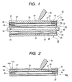
- FIG. 1 is a schematic sectional view of a liquid crystal display device that is one embodiment of an image display device according to the present invention.
- the liquid crystal display device 10 comprises a liquid crystal display unit 20, and an analog resistive film type touch panel (a coordinate input device) 30, which is one embodiment of the present invention, arranged on the front side thereof.
- a liquid crystal layer 23 is interposed between an upper substrate 21 and a lower substrate 22, which are arranged to face each other, and is sealed with a sealing material 24.
- a liquid crystal control layer 26 having electrodes, alignment films and the like is formed on the inner side (on the liquid crystal layer 23 side) of the upper substrate 21.
- a reflecting layer 27 including a thin films made of a metal having high reflectance, such as aluminum or silver, and a liquid crystal control layer 28 having electrodes, alignment films and the like are sequentially laminated on the lower substrate 22.
- the liquid crystal display unit 20 is of a reflective type that performs display by reflecting the external light incident from the outside by the reflecting layer 27.
- an upper light-transmitting substrate (a second light-transmitting substrate; operational substrate) 31 and a lower light-transmitting substrate (a first light-transmitting substrate or a fixed substrate) 32 are arranged to face each other and are integrally bonded to each other with a substantially annular adhesive layer 36, and a spatial portion is defined between the upper light-transmitting substrate 31 and the lower light-transmitting substrate 32.
- the upper light-transmitting substrate 31 is made of a flexible material, such as a transparent film.
- the lower light-transmitting substrate 32 is comprised of a transparent glass substrate, a plastic substrate, or a plastic film.
- a first transparent conductive film 33 is formed on the inner side (the upper light-transmitting substrate 31 side) of the lower light-transmitting substrate 32, and spacers comprised of an insulating layer (insulator) are formed on the first transparent conductive film 33 so as to be spaced apart from each other.
- the upper light-transmitting substrate 31 and the lower light-transmitting substrate 32 face each other with the insulating layer interposed therebetween.
- the printed circuit 37 is connected to the first transparent conductive film 33.
- a decorative printing layer 41 is formed at the periphery of the upper light-transmitting substrate 31 on the inner side (on the lower light-transmitting substrate 32 side). thereof.
- the decorative printing layer 41 is formed as a thin layer by a printing method, such as a screen printing method, a gravure printing method, and an offset printing method, a transfer method, or a vapor deposition method.
- the decorative printing layer 41 is formed by performing a decorating process to form a decoration, such as a pattern, a character, a mark, a design, or a color.
- the thickness of the decorative printing layer 41 is, for example, about 0.01 to 100 ⁇ m.
- the decorative printing layer 41 is located at the upper side of the lower printed circuit (the first printed circuit) 37 and the upper printed circuit (the second printed circuit) 38, which will be described later.
- the touch panel 30 is seen from the upper transparent substrate 31 side (the operation surface of the second transparent substrate)
- the lower printed circuit (the first printed circuit) 37 and the upper printed circuit (the second printed circuit) to be mentioned later are concealed by the decorative printing layer 41, such that they cannot be seen by visual observation.
- the decorative printing layer 41 is formed as a thin layer, there is little step difference between the inner surface of the upper light-transmitting substrate 31 and the decorative printing layer 41.
- the inner surface of the upper light-transmitting substrate 31 and the decorative printing layer 41 are covered by an overcoat layer 42 which is more transparent.
- an ultraviolet curable acrylic resin-cured layer or a siliceous layer of a polysilazame-containing compound and the like can be exemplified.
- the substance of the overcoat layer 42 it is preferable to use a substance which has an excellent adhesiveness with the decorative printing layer 41, a second transparent conductive film 34 to be mentioned later, and the upper light-transmitting substrate 31 to increase the adhesiveness between the second transparent conductive film 34 and the decorative printing layer 41.
- the overcoat layer 42 can also be formed by an in-mold molding method, which will be described later, in addition to the printing method, the transfer method, and the vapor deposition method.
- the second transparent conductive film 34 is formed on the inner side of the overcoat layer 42.
- the first and second transparent conductive films 32 and 34 are made of indium tin oxide (ITO) or the like.
- the upper printed circuit (the second printed circuit) 38 comprising a lead-out circuit of a conductive paste which is obtained by dispersing conductive metallic fillers in a resin, a connecting electrode portion connected to the lead-out circuit and the like is formed at the peripheral portion of the upper light-transmitting substrate 31 on the inner side thereof.
- the second transparent conductive film 34 is connected to the printed circuit 38.
- the overcoat layer 42 is formed by an in-mold molding method, first, a transfer film comprised of a supporting sheet and the decorative printing layer 41 formed on one surface of the supporting sheet are prepared. The decorative printing layer 41 is transferred to the upper transparent substrate 31 from the transfer film. Then, the upper transparent substrate 31 is placed in a metallic mold for injection molding. Subsequently, a resin having an excellent adhesiveness with the substrate 31 and the like is injected into the metallic mold to thus form the overcoat layer 42.
- the touch panel 30 is fixed to the liquid crystal display unit 20 with the supporting member 39 interposed therebetween. In the state of the touch panel 30 being fixed, the touch panel 30 and the liquid display unit 20 are spaced apart from each other with a predetermined gap.
- the touch panel 30 having the above-mentioned configuration is of resistive contact type.
- the first and second transparent conductive films 33 and 34 which are spaced by the film forming thickness of the adhesive layer 36, the printed circuit 37 and 38 or the spacers, are bent by pressing the upper transparent substrate 31 using an indicator 40 or the like.
- the first and second transparent conductive film 33 and 34 are electrically connected to each other.
- a voltage is alternately applied to the printed circuits 37 and 38.
- a coordinate at the pressed position can be detected by detecting the voltage output from the printed circuit to which the voltage is not applied.
- the liquid crystal display device 10 having such a configuration, it is possible to perform display using the liquid crystal display unit 20. Furthermore, it is possible to perform coordinate input by scanning the operating surface (the surface of the upper light-transmitting substrate 31) of the touch panel 30 using the indicator 40 (a pen-type indicator in the figure). Therefore, for example, when an operation is performed for selecting an object such as menu items displayed on the liquid crystal display unit 20, the selection operation is performed by pressing the displayed position of the object using the indicator 40.
- the decorative printing layer 41 is formed between the second transparent conductive film 34 formed on the inner side of the second transparent substrate 31 and the second light-transmitting substrate 34 such that the printed circuits 37 and 38 arranged at the periphery of the first and second light-transmitting substrates are concealed by the decorative printing layer 41.
- the decorative printing layer 41 is formed between the second transparent conductive film 34 formed on the inner side of the second transparent substrate 31 and the second light-transmitting substrate 34 such that the printed circuits 37 and 38 arranged at the periphery of the first and second light-transmitting substrates are concealed by the decorative printing layer 41.
- the decorative printing layer 41 is formed on the inner side of the second light-transmitting substrate 31, the outer surface of the second light-transmitting substrate 31 can be made flat. Therefore, it has no step difference with an operating surface, unlike a conventional touch panel in which a frame such as a bezel is arranged at the outer surface of the tablet. Thus, in the case of scanning the operating surface by using the indicator 40, there is no obstruction against the scanning operation, thereby allowing an easy operation.
- the decorative printing layer 41 can be formed by the above-mentioned printing method, transfer method, or vapor deposition method, it is possible to make the decorative printing layer thin. Also, there is little step difference between the inner surface of the second light-transmitting substrate 31 and the decorative printing layer 41. Therefore, it is possible to make the touch panel 30 according to the present invention thin compared to the conventional touch panel having a frame, such a bezel, on the outer surface of a tablet.
- the overcoat layer 42 is formed between the transparent conductive film 34 formed on the inner side of the second light-transmitting substrate 31 and the decorative printing layer 41. Therefore, it is possible to increase the flatness of the inner side of the second light-transmitting substrate 31.
- the flatness of the second light-transmitting substrate 31 at the outer side thereof is excellent, and the thin touch panel 30 is provided on the front side of the liquid crystal display unit 20, such that it is easy to input a coordinate by scanning the operation surface of the touch panel 30 using the indicator 40 or the like, it is possible to smoothly select objects such as menu items displayed on the liquid crystal display unit, and it is possible to make the liquid crystal display device thin.
- the light crystal display device 10 is provided with the touch panel 30 including the second light-transmitting substrate 31 having a flat outer surface, such that there is no step portion between the operating surface and the frame unlike the conventional tablet which has a frame such as bezel on the outer surface thereof. Thus, it is possible to prevent the adherence of dust caused by the step portion.
- the first and second printed circuits 37 and 38 are concealed by the decorative printing layer 41, such that the first and second printed circuit 37 and 38 are not seen from the outside and the touch panel has a good appearance.
- the touch panel 30 is arranged on the front side of the liquid crystal unit 20 as shown in FIG. 1.
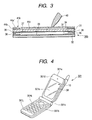
- a touch panel 30a shown in FIG. 2 and a touch panel 30b shown in FIG 3 may be used as the touch panel.
- the touch panel 30a shown in FIG. 2 is different from the touch panel 30 shown in FIG. 1 in that a decorative printing sheet 41a for concealing the first and second printed circuit 37 and 38 is formed at the periphery of the second light-transmitting substrate 31 on the outer side thereof, and a second printed circuit 37 connected to a second transparent conductive film 33 is formed at the periphery of the second light-transmitting substrate 31 on the inner side thereof.
- a decorative printing layer 44b such as a pattern, a character, a mark, a design and the like is formed on a sheet-like film 44a having a rectangular frame shape in plan view by a printing method such as a screen printing method, a gravure printing method, an offset printing method, a transfer method or a vapor deposition method.
- the thickness of the decorative printing sheet 41a is considerably small.
- an adhesive layer (not shown) is formed on the lower side of the decorative printing layer 44b.
- the thickness of the decorative printing sheet 41a is, for example, about 0.015 mm to 0.3 mm.
- the decorative printing sheet 41a before being arranged on the outer side of the second light-transmitting substrate 31, a surface thereof facing the adhesive layer is adhered on a supporting sheet.
- the decorative printing sheet 41a can be arranged on the outer surface of the second light-transmitting substrate 31 by attaching the surface facing the adhesive layer to the outer surface of the second light-transmitting substrate 31 after peeling off the supporting sheet.
- the overcoat layer 42 provided at the touch panel 30 in FIG. 1 is not formed at the inner side of the second light-transmitting substrate 31.
- the decorative printing sheet 41a is made thin such that there is little step difference between the outer surface of the second light-transmitting substrate 31 and the decorative printing sheet 41a. Therefore, as compared to the conventional touch panel having a frame such as a bezel on the outer surface of a tablet, the touch panel 30a shown in FIG. 2 can be made thinner.
- the touch panel 30b shown in FIG. 3 is different from the touch panel 30 shown in FIG. 1 in that a decorative printing sheet 41b for concealing the first and second printed circuit 37 and 38 is formed at the periphery of the second light-transmitting substrate 31 on the outer side thereof, and a second printed circuit 37 connected to the second transparent conductive film 33 is formed at the periphery of the second light-transmitting substrate 31 on the inner side thereof.
- a decorative printing layer 44b such as a pattern, a character, a mark, a design and the like is formed at the periphery of a sheet-like film 44a' having a rectangular frame shape in plan view by a printing method such as a screen printing method, a gravure printing method, an offset printing method, a transfer method, or a vapor deposition method.
- the thickness of the decorative printing sheet 41b is considerably small.
- an adhesive layer 44c is formed on the lower side of the sheet-like film 44a' and the decorative printing layer 44b.
- the decorative printing sheet 41b is particularly different from the decorative printing sheet 41a in that the shape of the sheet-like film is rectangular shape in plan view and in that the adhesive layer 44c is formed so as to cover the lower surface of the sheet-like film 44a' and the lower surface of the decorative printing layer 44b. Therefore, it is preferable for the adhesive layer 44c to have an excellent transparency and an excellent defoaming property.
- the thickness of the decorative printing sheet 41b is, for example, about 0.015 mm to 0.3 mm.
- the decorative printing sheet 41b before being arranged on the outer surface of the second light-transmitting substrate 31, a surface thereof facing the adhesive layer is adhered on a supporting sheet.
- the decorative printing sheet 41b can be formed on the outer surface of the second light-transmitting substrate 31 by attaching the surface facing the adhesive layer to the outer surface of the second light-transmitting substrate 31 after peeling off the supporting sheet.
- the decorative printing sheet described above is formed on outer surface of the second light-transmitting substrate 31, such that the printed circuits 37 and 38 are not seen when a user views the touch panel from the operation surface side of the second light-transmitting substrate 31. Furthermore, since the decoration is performed on the decorative printing sheet, the touch panel has a good appearance.
- the image display device is applied to the reflective liquid crystal display device.
- the image display device may be a liquid crystal display device in which a front light (an illumination device) is arranged between the coordinate input device and the liquid crystal display unit.
- FIG. 4 is a perspective view showing an example of a mobile phone (an electronic apparatus) comprising the liquid crystal display device of the previous embodiments related to the present invention.
- an upper case 301a are expandably connected to a lower case 301b by a hinge 301c, and a display unit 301e is installed on an operation surface 301d of the upper case 301a.
- the display unit 301e is provided with the liquid crystal display device 10 according to the above-mentioned embodiment while the touch panel 30 is directed upward.
- an operation surface 301j of the lower casing 301b is provided with an input keyboard 301k for performing dialing operation.
- the display unit 301e comprises the liquid crystal display device 10 of the previous embodiments, such that the mobile phone can be made as a thin type mobile phone of which appearance and convenience are improved and in which dust and the like is prevented from being attached to the display unit.
Landscapes
- Engineering & Computer Science (AREA)
- General Engineering & Computer Science (AREA)
- Theoretical Computer Science (AREA)
- Human Computer Interaction (AREA)
- Physics & Mathematics (AREA)
- General Physics & Mathematics (AREA)
- Position Input By Displaying (AREA)
- Liquid Crystal (AREA)
- Push-Button Switches (AREA)
Abstract
Description
- The present invention relates to a coordinate input device, an image display device comprising the coordinate input device, and an electronic apparatus comprising the coordinate input device. Particularly, the present invention relates to a coordinate input device in which an operation surface can be scanned using an indicator to input coordinates, an image display device comprising the coordinate input device, and an electronic apparatus comprising such an image display device.
- Recently, as a display unit for electronic apparatuses such as personal digital assistants (PDA), there is known a display unit in which a transparent tablet (or a touch panel) is arranged on the front side of a liquid crystal display unit so that a user can directly operate an object such as a menu item displayed on the display unit with his/her finger or an indicator.
- FIG. 5 is a sectional view illustrating an example of a liquid crystal display device comprising such a tablet.
- A liquid
crystal display device 100 shown in FIG. 5 is constructed such that atablet 130 is arranged on the front side of a liquidcrystal display unit 120. In the liquidcrystal display unit 120, aliquid crystal layer 123 is interposed between anupper substrate 121 and alower substrate 122, which are arranged to face each other and sealed with a sealing material 124b therebetween. A liquidcrystal control layer 126 having electrodes, alignment films and the like is formed on the inner side (theliquid crystal layer 123 side) of theupper substrate 121. On the inner side (liquid crystal layer 123 side) of thelower substrate 122, a reflecting layer including a thin film made of a metal having high reflectance, such as aluminum or silver, or atransflective layer 127 made of a metallic thin film in which through-holes are formed, and a liquidcrystal control layer 128 having electrodes, alignments films and the like are sequentially laminated on thelower substrate 122. - In the
tablet 130, upper and lowertransparent substrates adhesive layer 136. On the inner side (theupper substrate 131 side) of thelower substrate 132, afirst electrode layer 133 is formed. On the firsttransparent electrode layer 133, insulating spacers (not shown) are formed so as to be spaced apart from each other. On the inner side (lower substrate 132 side) of theupper substrate 131, a secondtransparent electrode layer 134 is formed. - A lower printed
circuit 137 including a lead-out circuit having a conductive paste which is made by dispersing conductive metallic fillers in a resin, a connecting electrode portion connected to the lead-out circuit and the like are formed on a peripheral portion of thelower substrate 132 at the inner side thereof. The printedcircuit 137 is connected to the firsttransparent electrode layer 133. Furthermore, an upper printedcircuit 138 including a lead-out circuit having a conductive paste which is made by dispersing conductive metallic fillers in a resin, a connecting electrode portion connected to the lead-out circuit and the like are formed on a peripheral portion of theupper substrate 131 at the inner side thereof. The printedcircuit 138 is connected to the secondtransparent electrode layer 134. - Further, in such type of
tablet 130, theupper substrate 131 has a transparent base, such that the printedcircuits upper substrate 131 on the inner side thereof, aframe 145, which is also referred to as a bezel, is provided so as to cover the printed circuit forming area (for example, see Japanese Unexamined Patent Application Publication No. 10-104374) - The
tablet 130 having the above construction is of a resistive contact type. Theupper substrate 131 is pressed with theindicator 140 so as to flex the first andsecond electrode layers adhesive layer 136 and the printedcircuits tablet 130 is not operated. Then, the first andsecond electrode layers - Further, the
tablet 130 is fixed to the liquidcrystal display unit 120 via supportingmembers 139, and in the state in which thetablet 130 is fixed, thetablet 130 and the liquidcrystal display unit 120 are spaced apart from each other with a predetermined gap therebetween. - According to the liquid
crystal display device 100 of the above-described construction, display can be performed using the liquidcrystal display unit 120, and the upper surface of thetablet 130 is scanned by the indicator 140 (a pen-type indicator in the drawing), such that coordinates can be input. Accordingly, when an operation is performed to select, for example, an object such as a menu item displayed on the liquidcrystal display unit 120, the selecting operation can be performed by pressing the displayed position of the object using theindicator 140. - However, in the liquid
crystal display device 100 having the above construction, since aframe 145 is arranged at the periphery of theupper substrate 131 of thetablet 130 on the outer side thereof, when the liquidcrystal display device 100 is installed, for example, in adisplay unit 601e of a mobile phone shown in FIG. 6, the thickness of the mobile phone increases. Furthermore, when a user views the display unit, theflame 145 is also observed, such that the appearance of the display unit deteriorates. - Further, when the above-mentioned
frame 145 is arranged on the upper surface of the tablet 130 (on the outer surface of the upper substrate 131), since a step portion exists between the operation surface (the outer surface of the upper substrate 131) and theframe 145, the scanning on the surface of thetablet 130 by theindicator 140 is often obstructed to hinder an easy operation, and dust easily attaches to the step portion. - The present invention has been made in consideration of the above circumstances, and an object of the present invention is to provide a coordinate input device, in which the appearance of the device is improved and the coordinate input operation is easily performed by scanning an operation surface using an indicator.
- Further, another object of the present invention is to provide an image display device comprising the above-mentioned coordinate input device capable of decreasing the thickness of an electronic apparatus, when the image display device is installed in a display unit of an electronic apparatus such as a mobile phone, and which is also capable of preventing the attachment of dust and the like in a step portion between a frame and an operation surface.
- Further, still another object of the present invention is to provide an electronic apparatus comprising the above-mentioned image display device, which has an improved appearance and convenience and which is capable of preventing the attachment of dust and the like on its display unit.
- The present invention employs the following construction to accomplish the above objects.
- In a coordinate input device according to a first aspect of the invention, a first light-transmitting substrate (a lower substrate on the fixed side) and a second light-transmitting substrate (an upper substrate on the operation side) oppose each other with an insulating layer interposed therebetween, the second light-transmitting substrate having its one surface serving as an operation surface, transparent conductive films are formed on respective inner sides of the light-transmitting substrates, printed circuits connected to the transparent conductive films are respectively formed at peripheries of the light-transmitting substrates, a voltage is alternately applied to the printed circuits formed on the first and second light-transmitting substrates, and an output voltage from the substrate to which the voltage is not applied is detected, such that a coordinate of a pressed position can be detected. A decorative printing layer is formed between the transparent conductive film formed on the inner side of the second light-transmitting substrate and the second light-transmitting substrate, and the printed circuits respectively formed at the peripheries of the first and second light-transmitting substrates are concealed by the decorative printing layer, such that the printed circuits cannot be viewed (visually seen) from the operation surface of the second light-transmitting substrate.
- According to the coordinate input device of the first aspect of the invention, the decorative printing layer is formed between the transparent conductive film formed on the inner side of the second light-transmitting substrate and the second light-transmitting substrate, and the printed circuits respectively formed at the peripheries of the first and second light-transmitting substrates are concealed by the decorative printing layer, such that the printed circuits cannot be viewed from the operation surface of the second light-transmitting substrate. Furthermore, on the decorative printing layer, a decoration such as a pattern, a character, a mark, a design, or a color is provided, such that the appearance thereof is improved.
- Further, since the decorative printing layer is formed on the inner side of the second light-transmitting substrate, an outer surface (an operation surface) of the second light-transmitting substrate can be made into a flat surface, and has no step portion which is prevalent in the conventional type in which a frame such as a bezel is provided on the outer surface of the tablet. Therefore, the scanning on the outer surface (operation surface) of the second light-transmitting substrate using an indicator and the like is not obstructed to allow an easy operation. Furthermore, since the outer surface of the second light-transmitting substrate can be made into a flat surface, a hard coating layer having abrasion resistance can be provided on the outer surface of the second light-transmitting substrate. Therefore, the second light-transmitting substrate can be protected by the hard coating layer.
- Further, since the decorative printing layer can be formed by a printing method such as a screen printing method, a gravure printing method, and an offset printing method, a transfer method, or a vapor deposition method, the thickness of the decorative printing sheet is made small and the step difference between the inner surface of the second light-transmitting substrate and the decorative printing layer does not appear. Therefore, the coordinate input device of the first aspect can be made thinner than the conventional type coordinate input devices having a frame such as a bezel on the outer surface of the tablet.
- Further, in the coordinate input device of the first aspect, it is preferable that a transparent overcoat layer is provided between the transparent conductive film formed on the inner side of the second light-transmitting substrate and the decorative printing layer. By providing such a transparent overcoat layer, the flatness of the second light-transmitting substrate at the inner side thereof can be improved, such that it is possible to favorably form the transparent conductive film on the inner side of the second light-transmitting substrate.
- Further, it is preferable that, as a material of the overcoat layer, a material having a good adherence to the decorative printing layer, the transparent conductive film, and the second light-transmitting substrate is used to increase the adherence between the transparent conductive film and the decorative printing layer.
- In a coordinate input device according to a second aspect of the invention, a first light-transmitting substrate (a lower substrate on the fixed side) and a second light-transmitting substrate (an upper substrate on the operation side) oppose each other with an insulating layer interposed therebetween, the second light-transmitting substrate having its one surface serving as an operation surface, transparent conductive films are formed on respective inner sides of the light-transmitting substrates, printed circuits connected to the transparent conductive films are respectively formed at peripheries of the light-transmitting substrates, a voltage is alternately applied to the printed circuits formed on the first and second light-transmitting substrates, and an output voltage from the substrate to which the voltage is not applied is detected, such that a coordinate of a pressed position can be detected.
- A decorative printing sheet is formed on an outer surface of the second light-transmitting substrate, and the printed circuits respectively formed at the peripheries of the first and second light-transmitting substrates are concealed by the decorative printing sheet, such that the printed circuits cannot be viewed from the operation surface of the second light-transmitting substrate.
- According to the coordinate input device of the second aspect, the decorative printing sheet is formed on the outer surface of the second light-transmitting substrate, such that the printed circuits cannot be viewed from the operation surface of the second light-transmitting substrate. Furthermore, on the decorative printing layer, a decoration such as a pattern, a character, a mark, or a design is provided, such that the appearance thereof is improved.
- Further, even though the decorative printing sheet is formed on the outer surface of the second light-transmitting substrate, the decorative printing sheet has a sheet-like shape, such that it is possible to make the thickness thereof extremely thin. Therefore, the outer surface of the second light-transmitting substrate becomes substantially a flat surface. Thus, the scanning on the outer surface of the second light-transmitting substrate using an indicator and the like is not obstructed to allow an easy operation. Furthermore, since the outer surface of the second light-transmitting substrate can be made into a substantially flat surface, a hard coating layer having abrasion resistance can be provided on the outer surface of the second light-transmitting substrate. Therefore, the second light-transmitting substrate can be protected by the hard coating layer.
- Further, in the decorative printing sheet, since a decoration such as a pattern, a character, a mark, a design or the like can be provided on a sheet-like film (base) by a printing method such as a screen printing method, a gravure printing method, and an offset printing method, a transfer method, or a deposition method, the thickness of the decorative printing sheet is made extremely small and there is little step difference between the outer surface of the second light-transmitting substrate and the decorative printing sheet. Therefore, the coordinate input device of the second aspect can be made thinner than the conventional type coordinate input devices having a frame such as a bezel on the outer surface of the tablet.
- Further, an adhesive layer may be formed one surface of the decorative printing sheet. In this case, the decorative printing sheet before being provided on the outer surface of the second light-transmitting substrate may be adhered to a supporting sheet with an adhesive layer interposed therebetween. The decorative printing sheet can be arranged on the outer surface of the second light-transmitting substrate by attaching the adhesive layer side surface to the second light-transmitting substrate after peeling off the supporting sheet.
- An image display device according to a third aspect of the invention comprises the coordinate input device of the present invention according to any one of the above constructions on the front side of the image display device such as a liquid crystal display device and an organic electro-luminescent (EL) display device.
- According to the image display device of the third aspect comprising the coordinate input device of the present invention according to any one of the above constructions on the front side of the image display device in which the outer surface of the second light-transmitting substrate has a good flatness and the coordinate input device is made thin, it is easy to input coordinates by scanning the operation surface of the coordinate input device with an indicator, it is possible to smoothly select objects such as menu items displayed on the image display unit, and the image display device can be made thin. Furthermore, since the image display device is provided with the coordinate input device in which the outer surface of the second light-transmitting substrate has a good flatness, there is no step portion which is prevalent in the conventional type in which a frame such as a bezel is arranged on the outer surface of the tablet. Therefore, it is possible to prevent the adherence of dust and the like in the step portion.
- Further, since the image display device is provided with the coordinate input device according to the present invention in which printed circuits are concealed by the decorative printing layer or the decorative printing sheet, the printed circuits cannot be viewed from the outside. Therefore, the appearance of the image display device is improved.
- An electronic apparatus of the fourth aspect comprises the image display device of the third aspect on its display unit.
- According to the electronic apparatus of the fourth aspect, since the electronic apparatus is provided with the image display device of the third aspect, the appearance of the electronic apparatus is improved to allow an easy operation, and it is possible to prevent dust and the like from being attached to the display unit.
- According to the present invention as described above, it is possible to provide a coordinate input device capable of improving the appearance of the device and which is also capable of easily inputting coordinates by scanning an operation surface using an indicator.
- Further, according to the above-mentioned image display device, since the image display device is provided with the coordinate input device according to the present invention, when the image display device is mounted on a display unit of an electronic apparatus such as a mobile phone, it is possible to make the electronic apparatus thin, and to prevent the adherence of dust and the like in a step portion between an operation surface and a frame.
- Further, since an electronic apparatus of the present invention comprises the image display device of the present invention, it is possible to provide a thin type electronic apparatus having improved appearance and convenience, and which is capable of preventing the adherence of dust and the like on the display unit.
-
- FIG. 1 is a schematic sectional view showing an embodiment of a liquid crystal display device comprising a coordinate input device related to the present invention;
- FIG. 2 is a schematic sectional view showing another embodiment of a coordinate input device related to the present invention;
- FIG. 3 is a schematic sectional view showing still another embodiment of a coordinate input device related to the present invention;
- FIG. 4 is a perspective view showing an example of an electronic apparatus comprising a liquid crystal display device related to the present invention;
- FIG. 5 is a sectional view showing an example of a liquid crystal display device comprising a conventional tablet; and
- FIG. 6 is a sectional view showing an example of a mobile phone comprising a conventional liquid crystal device on a display unit thereof.
-
- Embodiments of the present invention will now be described with reference to the drawings. In all the following drawings, scales of the film thickness or dimensions of respective elements are made appropriately different from each other in order to easily see the drawings.
- FIG. 1 is a schematic sectional view of a liquid crystal display device that is one embodiment of an image display device according to the present invention.
- The liquid
crystal display device 10 comprises a liquidcrystal display unit 20, and an analog resistive film type touch panel (a coordinate input device) 30, which is one embodiment of the present invention, arranged on the front side thereof. - In the liquid
crystal display unit 20, aliquid crystal layer 23 is interposed between anupper substrate 21 and alower substrate 22, which are arranged to face each other, and is sealed with a sealingmaterial 24. A liquidcrystal control layer 26 having electrodes, alignment films and the like is formed on the inner side (on theliquid crystal layer 23 side) of theupper substrate 21. On the inner side (on theliquid crystal layer 23 side) of thelower substrate 22, a reflectinglayer 27 including a thin films made of a metal having high reflectance, such as aluminum or silver, and a liquidcrystal control layer 28 having electrodes, alignment films and the like are sequentially laminated on thelower substrate 22. - The liquid
crystal display unit 20 is of a reflective type that performs display by reflecting the external light incident from the outside by the reflectinglayer 27. - In the
touch panel 30, an upper light-transmitting substrate (a second light-transmitting substrate; operational substrate) 31 and a lower light-transmitting substrate (a first light-transmitting substrate or a fixed substrate) 32 are arranged to face each other and are integrally bonded to each other with a substantially annularadhesive layer 36, and a spatial portion is defined between the upper light-transmittingsubstrate 31 and the lower light-transmittingsubstrate 32. The upper light-transmittingsubstrate 31 is made of a flexible material, such as a transparent film. The lower light-transmittingsubstrate 32 is comprised of a transparent glass substrate, a plastic substrate, or a plastic film. - A first transparent
conductive film 33 is formed on the inner side (the upper light-transmittingsubstrate 31 side) of the lower light-transmittingsubstrate 32, and spacers comprised of an insulating layer (insulator) are formed on the first transparentconductive film 33 so as to be spaced apart from each other. The upper light-transmittingsubstrate 31 and the lower light-transmittingsubstrate 32 face each other with the insulating layer interposed therebetween. - A lower printed circuit (a first printed circuit) 37 including a lead-out circuit having a conductive paste which is made by dispersing conductive metallic fillers in a resin and a connecting electrode portion connected to the lead-out circuit and the like is formed at the peripheral portion of the lower light-transmitting
substrate 32 on the inner side thereof. The printedcircuit 37 is connected to the first transparentconductive film 33. - A
decorative printing layer 41 is formed at the periphery of the upper light-transmittingsubstrate 31 on the inner side (on the lower light-transmittingsubstrate 32 side). thereof. Thedecorative printing layer 41 is formed as a thin layer by a printing method, such as a screen printing method, a gravure printing method, and an offset printing method, a transfer method, or a vapor deposition method. Thedecorative printing layer 41 is formed by performing a decorating process to form a decoration, such as a pattern, a character, a mark, a design, or a color. The thickness of thedecorative printing layer 41 is, for example, about 0.01 to 100 µm. - The
decorative printing layer 41 is located at the upper side of the lower printed circuit (the first printed circuit) 37 and the upper printed circuit (the second printed circuit) 38, which will be described later. When thetouch panel 30 is seen from the uppertransparent substrate 31 side (the operation surface of the second transparent substrate), the lower printed circuit (the first printed circuit) 37 and the upper printed circuit (the second printed circuit) to be mentioned later are concealed by thedecorative printing layer 41, such that they cannot be seen by visual observation. - Since the
decorative printing layer 41 is formed as a thin layer, there is little step difference between the inner surface of the upper light-transmittingsubstrate 31 and thedecorative printing layer 41. However, in order to further increase flatness, the inner surface of the upper light-transmittingsubstrate 31 and thedecorative printing layer 41 are covered by anovercoat layer 42 which is more transparent. As thetransparent overcoat layer 42, an ultraviolet curable acrylic resin-cured layer or a siliceous layer of a polysilazame-containing compound and the like can be exemplified. Furthermore, as the substance of theovercoat layer 42, it is preferable to use a substance which has an excellent adhesiveness with thedecorative printing layer 41, a second transparentconductive film 34 to be mentioned later, and the upper light-transmittingsubstrate 31 to increase the adhesiveness between the second transparentconductive film 34 and thedecorative printing layer 41. Theovercoat layer 42 can also be formed by an in-mold molding method, which will be described later, in addition to the printing method, the transfer method, and the vapor deposition method. - The second transparent
conductive film 34 is formed on the inner side of theovercoat layer 42. The first and second transparentconductive films - Further, the upper printed circuit (the second printed circuit) 38 comprising a lead-out circuit of a conductive paste which is obtained by dispersing conductive metallic fillers in a resin, a connecting electrode portion connected to the lead-out circuit and the like is formed at the peripheral portion of the upper light-transmitting
substrate 31 on the inner side thereof. The second transparentconductive film 34 is connected to the printedcircuit 38. - When the
overcoat layer 42 is formed by an in-mold molding method, first, a transfer film comprised of a supporting sheet and thedecorative printing layer 41 formed on one surface of the supporting sheet are prepared. Thedecorative printing layer 41 is transferred to the uppertransparent substrate 31 from the transfer film. Then, the uppertransparent substrate 31 is placed in a metallic mold for injection molding. Subsequently, a resin having an excellent adhesiveness with thesubstrate 31 and the like is injected into the metallic mold to thus form theovercoat layer 42. - Further, the
touch panel 30 is fixed to the liquidcrystal display unit 20 with the supportingmember 39 interposed therebetween. In the state of thetouch panel 30 being fixed, thetouch panel 30 and theliquid display unit 20 are spaced apart from each other with a predetermined gap. - The
touch panel 30 having the above-mentioned configuration is of resistive contact type. When thetouch panel 30 is not operated, the first and second transparentconductive films adhesive layer 36, the printedcircuit transparent substrate 31 using anindicator 40 or the like. At the pressed position, the first and second transparentconductive film circuits - According to the liquid
crystal display device 10 having such a configuration, it is possible to perform display using the liquidcrystal display unit 20. Furthermore, it is possible to perform coordinate input by scanning the operating surface (the surface of the upper light-transmitting substrate 31) of thetouch panel 30 using the indicator 40 (a pen-type indicator in the figure). Therefore, for example, when an operation is performed for selecting an object such as menu items displayed on the liquidcrystal display unit 20, the selection operation is performed by pressing the displayed position of the object using theindicator 40. - In the
touch panel 30 having such a construction, thedecorative printing layer 41 is formed between the second transparentconductive film 34 formed on the inner side of the secondtransparent substrate 31 and the second light-transmittingsubstrate 34 such that the printedcircuits decorative printing layer 41. Thus, when a user sees thetouch panel 30 from the operating surface side of the second light-transmitting substrate (the upper side of the second light-transmitting substrate), the first and second printedcircuits decorative printing layer 41, which makes a good appearance. - Further, since the
decorative printing layer 41 is formed on the inner side of the second light-transmittingsubstrate 31, the outer surface of the second light-transmittingsubstrate 31 can be made flat. Therefore, it has no step difference with an operating surface, unlike a conventional touch panel in which a frame such as a bezel is arranged at the outer surface of the tablet. Thus, in the case of scanning the operating surface by using theindicator 40, there is no obstruction against the scanning operation, thereby allowing an easy operation. - Further, since the
decorative printing layer 41 can be formed by the above-mentioned printing method, transfer method, or vapor deposition method, it is possible to make the decorative printing layer thin. Also, there is little step difference between the inner surface of the second light-transmittingsubstrate 31 and thedecorative printing layer 41. Therefore, it is possible to make thetouch panel 30 according to the present invention thin compared to the conventional touch panel having a frame, such a bezel, on the outer surface of a tablet. - Further, in the
touch panel 30 according to the present invention, theovercoat layer 42 is formed between the transparentconductive film 34 formed on the inner side of the second light-transmittingsubstrate 31 and thedecorative printing layer 41. Therefore, it is possible to increase the flatness of the inner side of the second light-transmittingsubstrate 31. - In the liquid
crystal display device 10 according to the present embodiment, the flatness of the second light-transmittingsubstrate 31 at the outer side thereof is excellent, and thethin touch panel 30 is provided on the front side of the liquidcrystal display unit 20, such that it is easy to input a coordinate by scanning the operation surface of thetouch panel 30 using theindicator 40 or the like, it is possible to smoothly select objects such as menu items displayed on the liquid crystal display unit, and it is possible to make the liquid crystal display device thin. Furthermore, the lightcrystal display device 10 is provided with thetouch panel 30 including the second light-transmittingsubstrate 31 having a flat outer surface, such that there is no step portion between the operating surface and the frame unlike the conventional tablet which has a frame such as bezel on the outer surface thereof. Thus, it is possible to prevent the adherence of dust caused by the step portion. - Further, in the
touch panel 30, the first and second printedcircuits decorative printing layer 41, such that the first and second printedcircuit - In the liquid crystal display device according to the above-mentioned embodiment, the
touch panel 30 is arranged on the front side of theliquid crystal unit 20 as shown in FIG. 1. However, atouch panel 30a shown in FIG. 2 and atouch panel 30b shown in FIG 3 may be used as the touch panel. - The
touch panel 30a shown in FIG. 2 is different from thetouch panel 30 shown in FIG. 1 in that adecorative printing sheet 41a for concealing the first and second printedcircuit substrate 31 on the outer side thereof, and a second printedcircuit 37 connected to a second transparentconductive film 33 is formed at the periphery of the second light-transmittingsubstrate 31 on the inner side thereof. - In the
decorative printing sheet 41a, adecorative printing layer 44b such as a pattern, a character, a mark, a design and the like is formed on a sheet-like film 44a having a rectangular frame shape in plan view by a printing method such as a screen printing method, a gravure printing method, an offset printing method, a transfer method or a vapor deposition method. The thickness of thedecorative printing sheet 41a is considerably small. Furthermore, on the lower side of thedecorative printing layer 44b, an adhesive layer (not shown) is formed. The thickness of thedecorative printing sheet 41a is, for example, about 0.015 mm to 0.3 mm. - In the
decorative printing sheet 41a before being arranged on the outer side of the second light-transmittingsubstrate 31, a surface thereof facing the adhesive layer is adhered on a supporting sheet. Thedecorative printing sheet 41a can be arranged on the outer surface of the second light-transmittingsubstrate 31 by attaching the surface facing the adhesive layer to the outer surface of the second light-transmittingsubstrate 31 after peeling off the supporting sheet. - Since the
decorative printing sheet 41a is arranged at the outer side of the second light-transmittingsubstrate 31, theovercoat layer 42 provided at thetouch panel 30 in FIG. 1 is not formed at the inner side of the second light-transmittingsubstrate 31. - Further, the
decorative printing sheet 41a is made thin such that there is little step difference between the outer surface of the second light-transmittingsubstrate 31 and thedecorative printing sheet 41a. Therefore, as compared to the conventional touch panel having a frame such as a bezel on the outer surface of a tablet, thetouch panel 30a shown in FIG. 2 can be made thinner. - The
touch panel 30b shown in FIG. 3 is different from thetouch panel 30 shown in FIG. 1 in that adecorative printing sheet 41b for concealing the first and second printedcircuit substrate 31 on the outer side thereof, and a second printedcircuit 37 connected to the second transparentconductive film 33 is formed at the periphery of the second light-transmittingsubstrate 31 on the inner side thereof. - In the
decorative printing sheet 41b, adecorative printing layer 44b such as a pattern, a character, a mark, a design and the like is formed at the periphery of a sheet-like film 44a' having a rectangular frame shape in plan view by a printing method such as a screen printing method, a gravure printing method, an offset printing method, a transfer method, or a vapor deposition method. The thickness of thedecorative printing sheet 41b is considerably small. Furthermore, on the lower side of the sheet-like film 44a' and thedecorative printing layer 44b, anadhesive layer 44c is formed. Thedecorative printing sheet 41b is particularly different from thedecorative printing sheet 41a in that the shape of the sheet-like film is rectangular shape in plan view and in that theadhesive layer 44c is formed so as to cover the lower surface of the sheet-like film 44a' and the lower surface of thedecorative printing layer 44b. Therefore, it is preferable for theadhesive layer 44c to have an excellent transparency and an excellent defoaming property. - The thickness of the
decorative printing sheet 41b is, for example, about 0.015 mm to 0.3 mm. - In the
decorative printing sheet 41b before being arranged on the outer surface of the second light-transmittingsubstrate 31, a surface thereof facing the adhesive layer is adhered on a supporting sheet. Thedecorative printing sheet 41b can be formed on the outer surface of the second light-transmittingsubstrate 31 by attaching the surface facing the adhesive layer to the outer surface of the second light-transmittingsubstrate 31 after peeling off the supporting sheet. - In the touch panels shown in FIGS. 2 and 3, the decorative printing sheet described above is formed on outer surface of the second light-transmitting
substrate 31, such that the printedcircuits substrate 31. Furthermore, since the decoration is performed on the decorative printing sheet, the touch panel has a good appearance. - The present invention is not limited to the above-described embodiments, and the present invention can be modified in various ways without departing from the sprit of the present invention.
- In the above-described embodiments, the image display device according to the present invention is applied to the reflective liquid crystal display device. However, the image display device may be a liquid crystal display device in which a front light (an illumination device) is arranged between the coordinate input device and the liquid crystal display unit.
- FIG. 4 is a perspective view showing an example of a mobile phone (an electronic apparatus) comprising the liquid crystal display device of the previous embodiments related to the present invention.
- In the
mobile phone 301 shown in FIG. 4, anupper case 301a are expandably connected to alower case 301b by ahinge 301c, and adisplay unit 301e is installed on anoperation surface 301d of theupper case 301a. Thedisplay unit 301e is provided with the liquidcrystal display device 10 according to the above-mentioned embodiment while thetouch panel 30 is directed upward. In addition, anoperation surface 301j of thelower casing 301b is provided with aninput keyboard 301k for performing dialing operation. - In the
mobile telephone 301 of the present embodiment, thedisplay unit 301e comprises the liquidcrystal display device 10 of the previous embodiments, such that the mobile phone can be made as a thin type mobile phone of which appearance and convenience are improved and in which dust and the like is prevented from being attached to the display unit.
Claims (7)
- A coordinate input device in which a first light-transmitting substrate and a second light-transmitting substrate oppose each other with an insulating layer interposed therebetween, the second light-transmitting substrate having its one surface serving as an operation surface; transparent conductive films are formed on respective inner sides of the light-transmitting substrates; printed circuits connected to the transparent conductive films are respectively formed at peripheries of the light-transmitting substrates; and a voltage is alternately applied to the printed circuits formed on the first and second light-transmitting substrates, and an output voltage from the substrate to which the voltage is not applied is detected, such that a coordinate of a pressed position can be detected,
wherein a decorative printing layer is formed between the transparent conductive film formed on the inner side of the second light-transmitting substrate and the second light-transmitting substrate; and
the printed circuits respectively formed at the peripheries of the first and second light-transmitting substrates are concealed by the decorative printing layer, such that the printed circuits cannot be viewed from the operation surface of the second light-transmitting substrate. - The coordinate input device according to claim 1,
a transparent overcoat layer is formed between the transparent conductive film formed on the inner side of the second light-transmitting substrate and the decorative printing layer. - The coordinate input device according to claim 1 or 2,
wherein the thickness of the decorative printing layer is from 0.01 µm to 100 µm. - A coordinate input device in which a first light-transmitting substrate and a second light-transmitting substrate oppose each other with an insulating layer interposed therebetween, the second light-transmitting substrate having its one surface serving as an operation surface; transparent conductive films are formed on respective inner sides of the light-transmitting substrates; printed circuits connected to the transparent conductive films are respectively formed at peripheries of the light-transmitting substrates; and a voltage is alternately applied to the printed circuits formed on the first and second light-transmitting substrates, and an output voltage from the substrate to which the voltage is not applied is detected, such that a coordinate of a pressed position can be detected,
wherein a decorative printing sheet is formed on an outer surface of the second light-transmitting substrate; and
the printed circuits respectively formed at the peripheries of the first and second light-transmitting substrates are concealed by the decorative printing sheet, such that the printed circuits cannot be viewed from the operation surface of the second light-transmitting substrate. - The coordinate input device according to claim 4,
wherein the thickness of the decorative printing sheet is from 0.015 mm to 0.3 mm. - An image display device comprising a coordinate input device according to claim 1 or 4 on a front side thereof.
- An electronic apparatus comprising, on its display unit, an image display device having a coordinate input device according to claim 1 or 4 on a front side thereof.
Applications Claiming Priority (2)
| Application Number | Priority Date | Filing Date | Title |
|---|---|---|---|
| JP2003413180A JP4545424B2 (en) | 2003-12-11 | 2003-12-11 | Coordinate input device and image display device and electronic apparatus provided with the same |
| JP2003413180 | 2003-12-11 |
Publications (2)
| Publication Number | Publication Date |
|---|---|
| EP1542121A2 true EP1542121A2 (en) | 2005-06-15 |
| EP1542121A3 EP1542121A3 (en) | 2009-04-22 |
Family
ID=34510541
Family Applications (1)
| Application Number | Title | Priority Date | Filing Date |
|---|---|---|---|
| EP04257525A Withdrawn EP1542121A3 (en) | 2003-12-11 | 2004-12-03 | Coordinate input device, image display device and electronic apparatus |
Country Status (4)
| Country | Link |
|---|---|
| US (1) | US20050146516A1 (en) |
| EP (1) | EP1542121A3 (en) |
| JP (1) | JP4545424B2 (en) |
| CN (1) | CN100357866C (en) |
Cited By (7)
| Publication number | Priority date | Publication date | Assignee | Title |
|---|---|---|---|---|
| EP1901530A1 (en) | 2006-09-15 | 2008-03-19 | LG Electronics Inc. | Mobile communication device |
| CN101576794B (en) * | 2009-06-05 | 2011-05-18 | 深圳莱宝高科技股份有限公司 | Capacitive touch screen and manufacturing method thereof |
| CN101384981B (en) * | 2006-02-10 | 2011-07-13 | 夏普株式会社 | Touch panel coordinate position detection device |
| EP2323025A3 (en) * | 2009-11-17 | 2015-03-25 | eTurboTouch Technology Inc. | Flat-surface resistive touch panel |
| EP2638454A4 (en) * | 2010-11-09 | 2015-11-04 | Tpk Touch Solutions Inc | TOUCH PANEL STACK |
| EP2495639A4 (en) * | 2009-10-30 | 2016-03-09 | Kyocera Corp | Input device and display device equipped with same |
| EP3686721A1 (en) * | 2019-01-23 | 2020-07-29 | Oike&Co., Ltd. | Decorative conductive film, resistance film type touch panel, and electronic device |
Families Citing this family (50)
| Publication number | Priority date | Publication date | Assignee | Title |
|---|---|---|---|---|
| JP2004227222A (en) * | 2003-01-22 | 2004-08-12 | Toshiba Corp | Electronics |
| JPWO2005064451A1 (en) * | 2003-12-26 | 2007-12-20 | 日本写真印刷株式会社 | Electronic devices with protective panels, protective panels |
| TW200910169A (en) * | 2007-08-24 | 2009-03-01 | Onetouch Technologies Co Ltd | Touch panel structure |
| TWI374379B (en) | 2007-12-24 | 2012-10-11 | Wintek Corp | Transparent capacitive touch panel and manufacturing method thereof |
| TWM348999U (en) * | 2008-02-18 | 2009-01-11 | Tpk Touch Solutions Inc | Capacitive touch panel |
| KR100894710B1 (en) * | 2008-06-27 | 2009-04-24 | (주) 월드비젼 | Window integrated touch screen and manufacturing method thereof |
| WO2010023870A1 (en) * | 2008-08-25 | 2010-03-04 | 信越ポリマー株式会社 | Input devices and electronic device using said input devices |
| KR101040802B1 (en) | 2009-01-16 | 2011-06-13 | 삼성모바일디스플레이주식회사 | Windows integrated touch screen panel |
| KR100942742B1 (en) * | 2009-02-27 | 2010-02-18 | 주식회사 토비스 | Touch panel |
| KR100950194B1 (en) * | 2009-03-13 | 2010-03-29 | 주식회사 토비스 | Touch panel |
| JP5316165B2 (en) * | 2009-03-30 | 2013-10-16 | 富士通株式会社 | Mobile terminal device |
| KR20100111340A (en) * | 2009-04-07 | 2010-10-15 | 조한용 | Resistive touch sensor integrated with window panel |
| JP5235769B2 (en) * | 2009-04-27 | 2013-07-10 | 株式会社ジャパンディスプレイイースト | Liquid crystal display |
| JP5652807B2 (en) * | 2009-06-11 | 2015-01-14 | レノボ・イノベーションズ・リミテッド(香港) | Backlight type display device for portable device |
| JP2012181563A (en) * | 2009-06-29 | 2012-09-20 | Alps Electric Co Ltd | Coordinate input device, display device having the same, and electronic apparatus |
| CN101943965B (en) * | 2009-07-08 | 2013-09-18 | 群康科技(深圳)有限公司 | Touch screen and electronic device therewith |
| KR101140377B1 (en) * | 2010-02-19 | 2012-05-03 | 주식회사 모린스 | touch screen panel and method for manufacturing touch screen panel |
| TW201145132A (en) * | 2010-03-11 | 2011-12-16 | Alps Electric Co Ltd | Translucent inputting device |
| CN102243543A (en) * | 2010-05-11 | 2011-11-16 | 昆山榕增光电科技有限公司 | Touch panel and manufacturing method thereof |
| TW201205383A (en) * | 2010-05-31 | 2012-02-01 | Wintek Corp | Touch-sensitive device |
| TWI456443B (en) * | 2010-06-07 | 2014-10-11 | Wintek Corp | Touch-sensitive device and touch-sensitive display device |
| KR101756656B1 (en) * | 2010-06-25 | 2017-07-11 | 엘지디스플레이 주식회사 | Organic light emitting diode display device including touch panel |
| CN103052931A (en) * | 2010-07-30 | 2013-04-17 | Lg伊诺特有限公司 | touch panel |
| TWI402027B (en) * | 2010-08-20 | 2013-07-11 | Qisda Corp | Electronic device with touch function |
| BR112013006786A2 (en) * | 2010-09-20 | 2019-09-24 | Printechnologics Gmbh | capacitive information carrier, method for producing a capacitive information carrier, system for acquiring information and use of a capacitive information carrier |
| TW201213949A (en) * | 2010-09-29 | 2012-04-01 | Catcher Technology Co Ltd | Touch panel |
| JP5406161B2 (en) | 2010-10-20 | 2014-02-05 | アルプス電気株式会社 | Input device and method for manufacturing input device |
| JP2012098785A (en) * | 2010-10-29 | 2012-05-24 | Alps Electric Co Ltd | Input device manufacturing method |
| KR101793073B1 (en) * | 2010-12-06 | 2017-11-03 | 삼성디스플레이 주식회사 | Touch Screen Panel |
| JP2011118409A (en) * | 2011-01-19 | 2011-06-16 | Hitachi Ltd | Display device and apparatus including the same |
| CN102662504B (en) | 2012-02-29 | 2015-02-18 | 南京瀚宇彩欣科技有限责任公司 | A touch control device |
| US20130300985A1 (en) * | 2012-05-14 | 2013-11-14 | Marcus Bulda | Integrated privacy filter |
| KR20130130368A (en) * | 2012-05-22 | 2013-12-02 | 삼성전자주식회사 | Liquid crystal panel and liquid crystal display apparatus |
| JP6146635B2 (en) * | 2012-08-29 | 2017-06-14 | 大日本印刷株式会社 | Front plate and method for manufacturing front plate |
| KR20140030727A (en) * | 2012-09-03 | 2014-03-12 | 삼성전기주식회사 | Touch panel and method for manufacturing the same |
| US9492994B2 (en) * | 2012-09-20 | 2016-11-15 | Tpk Touch Solutions Inc. | Device having multiple printing layers and a printing method thereof |
| CN103885626A (en) * | 2012-12-20 | 2014-06-25 | 瑞世达科技(厦门)有限公司 | Touch panel and cover plate structure thereof |
| KR20140081313A (en) * | 2012-12-21 | 2014-07-01 | 삼성전기주식회사 | Touch sensor |
| JP5385475B2 (en) * | 2013-03-26 | 2014-01-08 | 株式会社ジャパンディスプレイ | Mobile phone equipment |
| JP6185272B2 (en) * | 2013-04-12 | 2017-08-23 | 株式会社タカラインコーポレーション | Display device film, display device film manufacturing method and device, and image display device |
| WO2014185330A1 (en) * | 2013-05-15 | 2014-11-20 | 日本写真印刷株式会社 | Transparent conductor |
| JP5860837B2 (en) * | 2013-05-16 | 2016-02-16 | デクセリアルズ株式会社 | Capacitive touch panel |
| WO2015025710A1 (en) * | 2013-08-20 | 2015-02-26 | デクセリアルズ株式会社 | Capacitive touch panel and method for manufacturing same |
| JP5714678B2 (en) * | 2013-10-03 | 2015-05-07 | 株式会社ジャパンディスプレイ | Mobile phone equipment |
| US9677168B2 (en) * | 2013-10-08 | 2017-06-13 | TPK America, LLC | Touch panel and method for manufacturing the same |
| TW201520840A (en) * | 2013-11-26 | 2015-06-01 | Henghao Technology Co Ltd | Method of forming a touch panel |
| CN103761008B (en) * | 2014-01-18 | 2017-06-20 | 深圳莱宝高科技股份有限公司 | A kind of face equipment and preparation method thereof |
| CN104216565A (en) * | 2014-09-04 | 2014-12-17 | 上海和辉光电有限公司 | Display device and manufacturing method thereof |
| KR102669729B1 (en) | 2016-11-17 | 2024-05-28 | 삼성디스플레이 주식회사 | Display device and manufacturing method thereof |
| WO2019220749A1 (en) * | 2018-05-18 | 2019-11-21 | アルプスアルパイン株式会社 | Input device |
Citations (3)
| Publication number | Priority date | Publication date | Assignee | Title |
|---|---|---|---|---|
| US4907090A (en) | 1988-08-12 | 1990-03-06 | Fredrick Ananian | Projection television screen protector |
| WO2000070550A1 (en) | 1999-05-13 | 2000-11-23 | Nissha Printing Co., Ltd. | Low reflection touch panel |
| US20020090798A1 (en) | 2001-01-10 | 2002-07-11 | Young-Soo Ahn | Contact structure of substrates of touch panel and method of bonding the same |
Family Cites Families (16)
| Publication number | Priority date | Publication date | Assignee | Title |
|---|---|---|---|---|
| JPH0533242U (en) * | 1991-10-07 | 1993-04-30 | キヤノン株式会社 | Electronics |
| JPH05114329A (en) * | 1991-10-21 | 1993-05-07 | Nissha Printing Co Ltd | Transparent touch panel with display design |
| DE69423552T2 (en) * | 1993-08-10 | 2000-09-07 | Canon K.K., Tokio/Tokyo | Liquid crystal display |
| US5579036A (en) * | 1994-04-28 | 1996-11-26 | At&T Global Information Solutions Company | Touch screen device and shielding bracket therefor |
| JPH08152967A (en) * | 1994-11-30 | 1996-06-11 | Sanyo Electric Co Ltd | Operation display device |
| JPH0934624A (en) * | 1995-07-17 | 1997-02-07 | Seiko Denshi Kiki Kk | Coordinate reading device |
| JPH1166996A (en) * | 1997-08-12 | 1999-03-09 | Nissha Printing Co Ltd | Transparent touch panel having printing display part |
| JP2000047189A (en) * | 1998-07-28 | 2000-02-18 | Sharp Corp | Liquid crystal display device |
| JP2000056315A (en) * | 1998-08-06 | 2000-02-25 | Toshiba Corp | Liquid crystal display device |
| CA2278832A1 (en) * | 1999-01-06 | 2000-07-06 | Vtech Communications, Ltd. | Touch screen overlay apparatus |
| JP2000222126A (en) * | 1999-01-29 | 2000-08-11 | Denso Corp | Display device with touch panel |
| US6555235B1 (en) * | 2000-07-06 | 2003-04-29 | 3M Innovative Properties Co. | Touch screen system |
| CN2509621Y (en) * | 2001-07-25 | 2002-09-04 | 成都吉锐触摸电脑有限公司 | Frame type touch screen protective hood |
| US7242393B2 (en) * | 2001-11-20 | 2007-07-10 | Touchsensor Technologies Llc | Touch sensor with integrated decoration |
| JP3982283B2 (en) * | 2002-03-05 | 2007-09-26 | セイコーエプソン株式会社 | Display device and manufacturing method thereof |
| JP2003287739A (en) * | 2002-03-28 | 2003-10-10 | Nitto Denko Corp | LCD with touch panel |
-
2003
- 2003-12-11 JP JP2003413180A patent/JP4545424B2/en not_active Expired - Fee Related
-
2004
- 2004-11-30 US US10/999,600 patent/US20050146516A1/en not_active Abandoned
- 2004-12-03 EP EP04257525A patent/EP1542121A3/en not_active Withdrawn
- 2004-12-10 CN CNB2004101002528A patent/CN100357866C/en not_active Expired - Fee Related
Patent Citations (3)
| Publication number | Priority date | Publication date | Assignee | Title |
|---|---|---|---|---|
| US4907090A (en) | 1988-08-12 | 1990-03-06 | Fredrick Ananian | Projection television screen protector |
| WO2000070550A1 (en) | 1999-05-13 | 2000-11-23 | Nissha Printing Co., Ltd. | Low reflection touch panel |
| US20020090798A1 (en) | 2001-01-10 | 2002-07-11 | Young-Soo Ahn | Contact structure of substrates of touch panel and method of bonding the same |
Cited By (10)
| Publication number | Priority date | Publication date | Assignee | Title |
|---|---|---|---|---|
| CN101384981B (en) * | 2006-02-10 | 2011-07-13 | 夏普株式会社 | Touch panel coordinate position detection device |
| EP1901530A1 (en) | 2006-09-15 | 2008-03-19 | LG Electronics Inc. | Mobile communication device |
| RU2451980C2 (en) * | 2006-09-15 | 2012-05-27 | Эл Джи Электроникс Инк. | Mobile communication device |
| EP1901530B1 (en) * | 2006-09-15 | 2013-09-04 | LG Electronics Inc. | Mobile communication device |
| CN101576794B (en) * | 2009-06-05 | 2011-05-18 | 深圳莱宝高科技股份有限公司 | Capacitive touch screen and manufacturing method thereof |
| EP2495639A4 (en) * | 2009-10-30 | 2016-03-09 | Kyocera Corp | Input device and display device equipped with same |
| EP2323025A3 (en) * | 2009-11-17 | 2015-03-25 | eTurboTouch Technology Inc. | Flat-surface resistive touch panel |
| EP2638454A4 (en) * | 2010-11-09 | 2015-11-04 | Tpk Touch Solutions Inc | TOUCH PANEL STACK |
| US10691266B2 (en) | 2010-11-09 | 2020-06-23 | Tpk Touch Solutions, Inc. | Touch panel stackup |
| EP3686721A1 (en) * | 2019-01-23 | 2020-07-29 | Oike&Co., Ltd. | Decorative conductive film, resistance film type touch panel, and electronic device |
Also Published As
| Publication number | Publication date |
|---|---|
| CN1627318A (en) | 2005-06-15 |
| US20050146516A1 (en) | 2005-07-07 |
| CN100357866C (en) | 2007-12-26 |
| JP2005173970A (en) | 2005-06-30 |
| JP4545424B2 (en) | 2010-09-15 |
| EP1542121A3 (en) | 2009-04-22 |
Similar Documents
| Publication | Publication Date | Title |
|---|---|---|
| US20050146516A1 (en) | Coordinate input device, image display device, and electronic apparatus | |
| JP4896178B2 (en) | Coordinate input device and image display device and electronic apparatus provided with the same | |
| US9915979B2 (en) | Input device, display device, electronic device, and mobile terminal | |
| US7920225B2 (en) | Electronic apparatus with protective panel | |
| US9229600B2 (en) | Multi-touch active display keyboard | |
| JP5739857B2 (en) | Touch panel and method for manufacturing touch panel | |
| JP5095043B1 (en) | Display device with input function and electronic device | |
| JP5196973B2 (en) | Electronic equipment with panel-type input device | |
| KR101328832B1 (en) | Touch panel and touch screen having the same | |
| KR101094528B1 (en) | Protective panel with touch input | |
| US20110157065A1 (en) | Touch panel, display device, and electronic device | |
| JP5909560B2 (en) | Input device, display device, and electronic device | |
| CN104704458B (en) | Input device, display device and electronic device | |
| JP6014055B2 (en) | Input device, display device, and electronic device | |
| KR101012066B1 (en) | Pressure type touch screen pad for personal handheld device | |
| KR20080102446A (en) | Display protection combined touch switch | |
| JP5937307B2 (en) | Display device with input function and device | |
| CN102810018A (en) | Touch display panel | |
| KR20100111340A (en) | Resistive touch sensor integrated with window panel | |
| US20050052436A1 (en) | Coordinate input device, and liquid crystal display device and electronic apparatus comprising the same | |
| JP2004138416A (en) | Pressure-sensitive fingerprint sensor | |
| KR20090090098A (en) | Touch window and manufacturing method | |
| JP2013242775A (en) | Input unit, display unit and electronic device | |
| WO2011001828A1 (en) | Coordinate input device, a display device provided with the same, and electronic device | |
| JP2012248010A (en) | Input device, display apparatus, and equipment |
Legal Events
| Date | Code | Title | Description |
|---|---|---|---|
| PUAI | Public reference made under article 153(3) epc to a published international application that has entered the european phase |
Free format text: ORIGINAL CODE: 0009012 |
|
| AK | Designated contracting states |
Kind code of ref document: A2 Designated state(s): AT BE BG CH CY CZ DE DK EE ES FI FR GB GR HU IE IS IT LI LT LU MC NL PL PT RO SE SI SK TR |
|
| AX | Request for extension of the european patent |
Extension state: AL BA HR LV MK YU |
|
| PUAL | Search report despatched |
Free format text: ORIGINAL CODE: 0009013 |
|
| AK | Designated contracting states |
Kind code of ref document: A3 Designated state(s): AT BE BG CH CY CZ DE DK EE ES FI FR GB GR HU IE IS IT LI LT LU MC NL PL PT RO SE SI SK TR |
|
| AX | Request for extension of the european patent |
Extension state: AL BA HR LV MK YU |
|
| 17P | Request for examination filed |
Effective date: 20090915 |
|
| AKX | Designation fees paid |
Designated state(s): DE FR GB |
|
| 17Q | First examination report despatched |
Effective date: 20100202 |
|
| STAA | Information on the status of an ep patent application or granted ep patent |
Free format text: STATUS: THE APPLICATION IS DEEMED TO BE WITHDRAWN |
|
| 18D | Application deemed to be withdrawn |
Effective date: 20150701 |