EP1537623B1 - Antenna structures and their use in wireless communication devices - Google Patents
Antenna structures and their use in wireless communication devices Download PDFInfo
- Publication number
- EP1537623B1 EP1537623B1 EP03750727A EP03750727A EP1537623B1 EP 1537623 B1 EP1537623 B1 EP 1537623B1 EP 03750727 A EP03750727 A EP 03750727A EP 03750727 A EP03750727 A EP 03750727A EP 1537623 B1 EP1537623 B1 EP 1537623B1
- Authority
- EP
- European Patent Office
- Prior art keywords
- antenna
- ground portion
- antenna portions
- plates
- conducting
- Prior art date
- Legal status (The legal status is an assumption and is not a legal conclusion. Google has not performed a legal analysis and makes no representation as to the accuracy of the status listed.)
- Expired - Lifetime
Links
- 238000004891 communication Methods 0.000 title claims abstract description 34
- 230000005855 radiation Effects 0.000 claims abstract description 30
- 230000005540 biological transmission Effects 0.000 claims abstract description 4
- 229910052751 metal Inorganic materials 0.000 claims description 22
- 239000002184 metal Substances 0.000 claims description 22
- 239000003989 dielectric material Substances 0.000 claims description 9
- 239000004033 plastic Substances 0.000 claims description 8
- 229920003023 plastic Polymers 0.000 claims description 8
- 230000008878 coupling Effects 0.000 claims description 6
- 238000010168 coupling process Methods 0.000 claims description 6
- 238000005859 coupling reaction Methods 0.000 claims description 6
- 239000000463 material Substances 0.000 claims description 4
- 239000004020 conductor Substances 0.000 description 10
- 238000002955 isolation Methods 0.000 description 5
- 238000000926 separation method Methods 0.000 description 5
- 230000009977 dual effect Effects 0.000 description 4
- 239000011810 insulating material Substances 0.000 description 3
- 230000009467 reduction Effects 0.000 description 3
- PXHVJJICTQNCMI-UHFFFAOYSA-N Nickel Chemical compound [Ni] PXHVJJICTQNCMI-UHFFFAOYSA-N 0.000 description 2
- 230000005404 monopole Effects 0.000 description 2
- PEZNEXFPRSOYPL-UHFFFAOYSA-N (bis(trifluoroacetoxy)iodo)benzene Chemical compound FC(F)(F)C(=O)OI(OC(=O)C(F)(F)F)C1=CC=CC=C1 PEZNEXFPRSOYPL-UHFFFAOYSA-N 0.000 description 1
- 229910001316 Ag alloy Inorganic materials 0.000 description 1
- RYGMFSIKBFXOCR-UHFFFAOYSA-N Copper Chemical compound [Cu] RYGMFSIKBFXOCR-UHFFFAOYSA-N 0.000 description 1
- 229910000881 Cu alloy Inorganic materials 0.000 description 1
- 229910000861 Mg alloy Inorganic materials 0.000 description 1
- 229910000990 Ni alloy Inorganic materials 0.000 description 1
- 238000010521 absorption reaction Methods 0.000 description 1
- 238000005452 bending Methods 0.000 description 1
- 239000011248 coating agent Substances 0.000 description 1
- 238000000576 coating method Methods 0.000 description 1
- 230000000295 complement effect Effects 0.000 description 1
- 229910052802 copper Inorganic materials 0.000 description 1
- 239000010949 copper Substances 0.000 description 1
- 230000003993 interaction Effects 0.000 description 1
- 238000004519 manufacturing process Methods 0.000 description 1
- 239000007769 metal material Substances 0.000 description 1
- 238000007747 plating Methods 0.000 description 1
- 238000007493 shaping process Methods 0.000 description 1
- 239000000758 substrate Substances 0.000 description 1
Images

Classifications
-
- H—ELECTRICITY
- H01—ELECTRIC ELEMENTS
- H01Q—ANTENNAS, i.e. RADIO AERIALS
- H01Q21/00—Antenna arrays or systems
- H01Q21/24—Combinations of antenna units polarised in different directions for transmitting or receiving circularly and elliptically polarised waves or waves linearly polarised in any direction
-
- H—ELECTRICITY
- H01—ELECTRIC ELEMENTS
- H01Q—ANTENNAS, i.e. RADIO AERIALS
- H01Q1/00—Details of, or arrangements associated with, antennas
- H01Q1/12—Supports; Mounting means
- H01Q1/22—Supports; Mounting means by structural association with other equipment or articles
- H01Q1/24—Supports; Mounting means by structural association with other equipment or articles with receiving set
- H01Q1/241—Supports; Mounting means by structural association with other equipment or articles with receiving set used in mobile communications, e.g. GSM
- H01Q1/242—Supports; Mounting means by structural association with other equipment or articles with receiving set used in mobile communications, e.g. GSM specially adapted for hand-held use
- H01Q1/243—Supports; Mounting means by structural association with other equipment or articles with receiving set used in mobile communications, e.g. GSM specially adapted for hand-held use with built-in antennas
-
- H—ELECTRICITY
- H01—ELECTRIC ELEMENTS
- H01Q—ANTENNAS, i.e. RADIO AERIALS
- H01Q21/00—Antenna arrays or systems
- H01Q21/28—Combinations of substantially independent non-interacting antenna units or systems
-
- H—ELECTRICITY
- H01—ELECTRIC ELEMENTS
- H01Q—ANTENNAS, i.e. RADIO AERIALS
- H01Q9/00—Electrically-short antennas having dimensions not more than twice the operating wavelength and consisting of conductive active radiating elements
- H01Q9/04—Resonant antennas
- H01Q9/0407—Substantially flat resonant element parallel to ground plane, e.g. patch antenna
- H01Q9/0421—Substantially flat resonant element parallel to ground plane, e.g. patch antenna with a shorting wall or a shorting pin at one end of the element
Definitions
- the present invention relates to antenna structures used in wireless communication devices.
- the invention relates to portable communication devices such as handsets.
- Various antenna types are known for use in handheld communication devices. For example, monopole and dipole antennae, patch and so called planar inverted 'F' (PIF) antennae are all known for this application.
- Some modern wireless communication devices are designed for multi-mode use in more than one communication system. Generally, dedicated multiple antennae are required for use in each separate mode in which the device is to operate. In some cases, devices are to be designed for operating in more than one mode and this can require the overall antenna structure to be large. This is undesirable where there are practical space and size constraints on the antenna structure and on other components used in the device.
- some antenna structures operating in a so called space diversity arrangement include multiple active antenna portions even when they operate in a single communication mode or system.
- the space diversity arrrangement can require the overall antenna structure to be unduly large.
- WO 01 43183A describes a microwave antenna having a mounting device for securing a radiating patch on an antenna, the antenna including a housing of a rigid metallic material, a dielectric plate which is supported by the housing having on its surface a conducting ground plane which is coupled by conductive strips to the housing. An antenna is separated from the dielectric plate by plastic spacing elements.
- JP 2001 024426A describes an antenna device in which two patch electrodes forming antenna elements on an upper face of a dielectric substrate having a ground electrode on its lower face are employed in combination to generate circularly polarised radiation patterns.
- EP-A-1 148 584 describes a radio communication apparatus in which multiple antennas are provided to radiate with different polarisation components in switchable communication modes.
- the antennas are connected by conductors to a ground surface provided by a shielding case provided on a circuit board inside an insulating case.
- the purpose of the present invention is to provide a novel antenna structure including multiple active antenna portions suitable for use in a portable wireless communication device such as a mobile handset which facilitates use in multiple operational modes.
- a wireless communication device including an antenna structure, said antenna structure comprising
- the dielectric material providing a capacitive coupling between the metal covers and the ground portion may be a dielectric plastics layer.
- the dielectric material may have a permittivity of between 2.0 and 3.0, especially between 2.5 and 3.0.
- the antenna portions and the conducting ground portion may be conducting plates.
- the plates may for example be made partially (e.g. by surface plating or coating) or wholly of a highly conducting metal as used in the art, e.g. a nickel/silver alloy or copper or a copper alloy.
- the plates may all be formed from a single sheet of metal, e.g. by shaping and bending as illustrated later.
- the plate which forms the conducting ground portion may be a substantially rectangular plate and the plates which are antenna portions may be substantially square plates.
- the plates which are antenna portions may together define an envelope having an area not greater than that of the ground portion plate. Preferred sizes and relative separations of the plates are as described later.
- Two R.F. signal leads may be connected to the antenna structure in such a manner that a first conductor of each lead is connected to the first part of the conducting ground portion and a second conductor of each lead is connected to a respective one of the antenna portions.
- the leads, e.g. cables, may extend through respective holes in the first part of the conducting ground portion to contact the antenna portions.
- the antenna portions may provide so called PIF (planar inverted F) antennae which provide transmission of substantially omnidirectional R.F. radiation in a direction perpendicular to the radiating surface.
- PIF antennae are one of a variety of antenna forms which are known per se. However, their selection and use in the antenna structure of the invention is preferred for the reasons described later. Other known forms of antenna would be unsuitable for use in a high frequency multi-mode communications devices. For example, a multiple monopole antenna would require an unduly large space and it would be difficult to achieve a suitable isolation between the two antennae. Multiple dipole antennae would also require an unduly large space and would be complicated by their dual polarisation requirements.
- Patch antennae would require an unduly large space and would produce both polarisation and isolation problems which would be difficult to solve.
- Chip antennae formed on a dielectric would also be unsuitable because they would require an unduly large ground plane conductor and precise location of the antenna portions.
- the wireless communication device may for example be a handset for use in data communications. It may provide communications in a single operational mode, e.g. in a space diversity arrangement, or in two or more modes.
- the operational mode (or at least one of the operational modes) may be high frequency, e.g. having an operational frequency of 1 GHz or more, e.g. 2 to 5 GHz.
- the metal covers may be made of a known alloy of magnesium.
- the present invention beneficially is suitable for use in a multi-antenna communications device such as a mobile or portable handset terminal operating at one or more high frequencies and can surprisingly be provided in a form which is compact and space saving yet providing a good operational performance. It can give a good omnidirectional radiation pattern in azimuth cut and a high peak gain by each antenna portion. It can provide good isolation between the antenna portions. It may be produced in a relatively cheaply and easily form.
- FIGs. 1a and 1b show one known form of a typical PIF antenna.
- FIG.1a shows a plan view and FIG 1b shows a side view of the same antenna.
- the PIF antenna includes a conducting ground plane 1, a conducting radiation element 2 parallel to the ground plane 1, a dielectric insulating material 3 (which can be air) between these and a signal feed line 4.
- the feed line 4 includes an inner conductor and an outer conductor.
- the inner conductor connects the radiation element 2 to active R.F. transceiver circuitry (not shown).
- the outer conductor connects the ground plane 1 to active R.F. transceiver circuitry (not shown).
- a grounding pin 5 electrically connects the ground plane 1 and the radiation element 2.
- signals produced by the transceiver circuitry are fed via the feed line 4 to the radiation element 2 and are transmitted by the radiation element 2 into the surrounding space. Similarly incoming R.F. signals are picked up by the element 2 and passed for reception to the R.F. transceiver circuitry via the feed line 4.
- ground plane 1 has to have a minimum dimension of least ⁇ /4 and the radiation element 2 has to have a minimum dimension of ⁇ /8, where ⁇ is the mean wavelength of radiation to be transmitted or received.
- FIGs. 2a and 2b show a form of PIF antenna structure which includes multiple PIF radiating elements and a common ground plane.
- FIG. 2a shows a plan view
- FIG. 2b shows a side view of the same antenna structure.
- the PIF multiple antenna structure of FIGs. 2a and 2b includes a common ground plane 1, dual radiation elements 2a and 2b parallel to the ground plane 1, a dielectric insulating material 3 between these (again this can be air), signal feed lines 4a and 4b which connect the elements 2a, 2b respectively to active RF transceiver circuitry (not shown) and grounding pins 5a, 5b which electrically connect the ground plane 1 and the radiation elements 2a and 2b respectively.
- the signals produced by the transceiver circuitry are fed via the feed line 4a or 4b (whichever is activated by connection of a switch in the transceiver circuitry) to the appropriate radiation element 2a, 2b.
- the R.F. signals are transmitted by the radiation element 2a or 2b generally into the surrounding space.
- incoming R.F. signals are picked up by the element 2a or 2b and passed for reception to the R.F. transceiver via the feed line 4a or 4b as appropriate.
- Known theory shows that in order to avoid interaction between the two active radiation elements 2a and 2b there should be a separation of at least ⁇ /8 between these elements.
- the ground plane 1 (for two antennae) needs to have a minimum length of at least ⁇ /2.
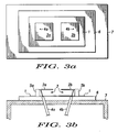
- FIGs. 3a and 3b show a form of multiple antenna structure embodying the invention which includes two PIF radiating elements and two ground planes.
- FIG. 3 shows a plan view and (b) shows a side view (partly in cross section) of the same antenna structure.
- Like items in FIGs. 2a and 2b and in FIGs. 3a and 3b have like reference numerals.
- the antenna structure of FIG 3 again includes a common ground plane 1, dual radiation elements 2a and 2b parallel to the ground plane 1, a dielectric insulating material 3 between these (again this can be air), signal feed lines 4a and 4b which connect the elements 2a, 2b respectively to active R.F.
- the structure shown in FIG. 3 includes also a conductive casing 7 (the second ground plane), which serves as a casing for various known components (for example active R.F. transceiver circuitry, not shown) of a communications handset of which the antenna structure forms a part.
- the casing 7 is shown in FIG. 3b as a sheet with perpendicular ends for simplicity but in practice will have a shape providing an encasing function as illustrated later.
- the ground plane 1 is separated from the casing 7 by a layer 6 of a dielectric material such as a layer of plastics material.
- the ground plane 1 is physically separated from, but capacitively coupled to, the conductive casing 7 via the layer 6.
- This coupling to the casing 7 allows the casing 7 to form part of the ground plane and effectively increases the ground plane surface area so allowing for an actual reduction in overall size of the physical multiple PIF antenna structure (components 1 to 5).
- a double element PIF antenna designed in the form shown in FIGs. 2a and 2b for use in known Bluetooth and data (IEEE 802.11b) communication applications, both of which use the 2.4 GHz frequency band, would normally require a ground plane surface area of about 62mm by 31 mm, which is ⁇ /2 by ⁇ /4.
- the conductive casing 7 of FIG. 3 may for example have a surface area of about 92mm by 30 mm, in other words approximately 150% of the normally required ground plane area.
- the plate forming the ground plane 1 can have a smaller physical multiple PIF antenna structure (components 1 to 5) allowing the plate forming the ground plane 1 to have a surface area of 49mm by 21 mm (in the 2.4 GHz example), which is 50% less than the normally required ground plane area in the antenna structure form shown in FIG. 2.
- the radiation elements 2a and 2b in the embodiment shown in FIGs. 2a and 2b may beneficially be increased in size to 19mm by 19mm mm from the dimensions of 15.5mm by 15.5 mm, which is ⁇ /8 by ⁇ /8, in order to increase the antenna gain.
- This embodiment of the invention allows the separation between the radiation elements to be reduced from the normally required 15.5 mm (at 2.4 GHz) in the FIG. 2 form, to only 10 mm in the FIG. 3 form, without impairing the performance of the two radiation elements 2a, 3a in the FIG. 3a/FIG.3b embodiment.
- the new antenna design includes all of the benefits of the standard PIFA design, including full control of impedance with VSWR better than 2, radiation pattern and polarisation by appropriate positioning of the radiation elements with respect to the ground plane edges, and positioning of the grounding pin and signal feed line.
- the two-antenna structure may have dual ⁇ (vertical/horizontal) polarisation to ensure good signal transfer regardless of the orientation of the device in which the two antenna structure is incorporated.
- FIGs. 4 to 11 illustrate use of a practical form of the two-antenna structure shown in FIG. 3 used in a communications handset.
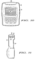
- FIGs. 4,10 and 11 show a data communications handset of the kind described in Applicant's copending International Patent Application having the published number WO03/021921A .
- the handset includes two metal covers 13, 15 (shown in FIG.10 ,11) which fit in rims of an insulating (plastics) carrier 12 (shown in FIG.10) with rubber cushioning rings also in the rims to provide mechanical protection to the covers when fitted to the carrier.
- the handset in FIG. 4 is labelled 11.
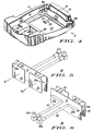
- FIG 4 shows the inside of the handset 11 with some components removed for clarity.
- the cushioning rings between the covers 13 and 15 and carrier are labelled 17 (FIG 4).
- the covers 13, 15 correspond to the second ground plane 7 shown in FIG. 3.
- Location recesses 16a, 16b provided on an inner wall of the cover 15 in the corner of the cover 15 also facilitate attachment of the cover 13 thereto by receipt of complementary corner studs (not shown) provided on an inner wall of the cover 13.
- An antenna housing 19 made of plastics material is fitted in a recess 21 formed in the casing structure provided by the covers 13. Together with the plastics carrier 12 separating the covers 13,15 the housing 19 serves as a dielectric coupling corresponding to the layer 6 of FIG. 3.
- the antenna housing 19 is at an end of the handset 11 which may be considered as its front end because radiation is transmitted from that end in use.
- the front facing outer surface of the antenna housing conveniently is flush with the front outer walls of the casing formed by the covers 13 and 15 so that the handset 11 has an overall smooth profile.
- Cables 23, 25 extend from the antenna housing 19 into the interior of the handset 11 and are connected to a R.F. portion of the handset 11 (not shown in FIG 1).
- the R.F. portion transmits and receives R.F. signals via an antenna structure, to be described below, located inside the housing 19.
- Other components such as a window 27 and circuit components 29 are seen in FIG.4 but will not be further described because they are not material to the present invention.
- FIG.s 5, 6, 7 and 8, and 9 show a two-antenna structure 26 which is incorporated in the antenna housing 19 of FIG 4 (this is not shown in FIGs. 5 to 9) with the cables 23 and 25 attached to the structure 26.
- the two-antenna structure 26 comprises two rectangular conducting plates 33, 35 considered to be at the front of the structure 26 and a larger plate 31 which is parallel with the plates 33, 35 and is located behind the plates 33,35 with respect to front of the structure 26 as indicated by forward directions X1 and X2.
- the plates 33 and 35 are coplanar.
- the plate 31 is electrically connected to the plates 33, 35 by conducting strips 37, 39 respectively.
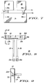
- FIG. 7 shows how the plates 31, 33 and 35 together with the strips 37 and 39 may be manufactured.
- a single sheet of metal is cut into the shape shown in FIG. 7 to provide the areas to be formed into the plates 31, 33 and 35 and the strips 37 and 39. The sheet is then bent along the axes indicated by broken lines Y1, Y2 shown in FIG. 7.
- the cables 23 and 25 are co-axial cables having at their ends distant from the plate 31 connectors 23a and 25a respectively.
- the cables 23 and 25 have metal outer conductors 23b and 25b respectively which are soldered to the rear face of the plate 31.
- Insulated wires 23c and 25c which are inside the conductors 23b and 25b respectively in the region behind the plate 31 extend from the sleeves 23b, 25b through holes 31a and 31b respectively formed in the plate 31.
- the insulated wire 23c is fed through a hole 33a (shown in FIGs. 5,7) in the plate 33 and an inner metal wire 23d protruding at the front end of the insulated wire 23c is soldered to the front face of the plate 33 as shown in FIG. 9.
- the insulated wire 25c is fed through a hole 35a (shown in FIG. 7) in the plate 35 and an inner metal wire 25d protruding at the front end of the insulated wire 25c is soldered to the front face of the plate 35.
- R.F. signals are produced in a transmit mode by the R.F. portion of the handset 1 and via the cable 23 or 25 as appropriate and are transmitted by the two antennas depending on the communication mode of the handset 1.
- incoming signals are received by the two antennas and are passed via the cable 23 or the cable 25 as appropriate to the R.F. portion of the handset.
- the first antenna including the plate 33 with ground plate 31
- the second antenna the plate 35 with ground plate 31
- the centre operational frequency used in each of these communication modes may for example be 2.4 GHz although other frequencies, e.g. typically 5GHz may be used as will be apparent to those familiar with the high frequency data communications field.
- the plate 31 and covers 13 and 15 (as second conducting ground portion) capacitively coupled thereto provide a common ground plane to both these antennas (plates 33 and 35) and thereby beneficially allow the antenna structure to operate in two different modes at high frequency yet beneficially to be constructed in a compact, space saving manner.
- the antenna structure shown in FIG.s 5 to 9 desirably has the following dimensions.
- the plate 31 desirably has an effective electrical length which is equivalent to at least 0.25 ⁇ , preferably 0.5 ⁇ , where ⁇ is the mean wavelength of radiation to be transmitted and received (for example, for one use where ⁇ is equivalent to 12,28cm; we have two different modes operating on one frequency band, 2.4- 2.485 GHz;).
- the plates 33 and 35 desirably have sides having an effective electrical length which is equivalent to at least 0.16 ⁇ .
- the plates 33 and 35 desirably have a separation distance equivalent to 0.073 ⁇ .
- the distance between the plate 31 and the plates 33 and 35 desirably is equivalent to 0.05 ⁇ .
- the shortest distance from the sides of the plates 33 and 35 to the metal of the covers 13 and 15 in the recess 16 is desirably equivalent to 0.05 ⁇ .
- the metal structure of the covers 13 and 15 thus beneficially provides an additional ground plane to the two antennas (plates 33 and 35) by capacitive coupling, thereby facilitating reduction in space and size of the antenna structure 26 and increased isolation between two antennas (plates 33 and 35).
- good antenna performance may be obtained by the antenna structure. For example, an antenna peak gain of +2-dBi and an average gain (over 360 degrees) of -4dBi in each of the two antennas (plates 33, 35) may be obtained and isolation of at least 12dB between these antennas (plates 33, 35) may be obtained. At the same time, a null in radiation pattern directed toward the rear of the handset of -2.0dB may be obtained which significantly reduces specific absorption rate (and causes the average gain to be less than the peak gain as stated).
Landscapes
- Engineering & Computer Science (AREA)
- Computer Networks & Wireless Communication (AREA)
- Support Of Aerials (AREA)
- Waveguide Aerials (AREA)
- Transceivers (AREA)
- Variable-Direction Aerials And Aerial Arrays (AREA)
- Details Of Aerials (AREA)
Abstract
Description
- The present invention relates to antenna structures used in wireless communication devices. In particular, the invention relates to portable communication devices such as handsets.
- Various antenna types are known for use in handheld communication devices. For example, monopole and dipole antennae, patch and so called planar inverted 'F' (PIF) antennae are all known for this application. Some modern wireless communication devices are designed for multi-mode use in more than one communication system. Generally, dedicated multiple antennae are required for use in each separate mode in which the device is to operate. In some cases, devices are to be designed for operating in more than one mode and this can require the overall antenna structure to be large. This is undesirable where there are practical space and size constraints on the antenna structure and on other components used in the device.
- In addition, some antenna structures operating in a so called space diversity arrangement include multiple active antenna portions even when they operate in a single communication mode or system. The space diversity arrrangement can require the overall antenna structure to be unduly large.
-
WO 01 43183A -
JP 2001 024426A -
EP-A-1 148 584 describes a radio communication apparatus in which multiple antennas are provided to radiate with different polarisation components in switchable communication modes. The antennas are connected by conductors to a ground surface provided by a shielding case provided on a circuit board inside an insulating case. - The purpose of the present invention is to provide a novel antenna structure including multiple active antenna portions suitable for use in a portable wireless communication device such as a mobile handset which facilitates use in multiple operational modes.
- According to the present invention there is provided a wireless communication device including an antenna structure, said antenna structure comprising
- a) a plurality of antenna portions each having a planar radiating surface;
- b) a planar conducting ground portion galvanically connected to each of the antenna portions;
- The dielectric material providing a capacitive coupling between the metal covers and the ground portion may be a dielectric plastics layer. The dielectric material may have a permittivity of between 2.0 and 3.0, especially between 2.5 and 3.0.
- The antenna portions and the conducting ground portion may be conducting plates. The plates may for example be made partially (e.g. by surface plating or coating) or wholly of a highly conducting metal as used in the art, e.g. a nickel/silver alloy or copper or a copper alloy. The plates may all be formed from a single sheet of metal, e.g. by shaping and bending as illustrated later. The plate which forms the conducting ground portion may be a substantially rectangular plate and the plates which are antenna portions may be substantially square plates. The plates which are antenna portions may together define an envelope having an area not greater than that of the ground portion plate. Preferred sizes and relative separations of the plates are as described later.
- Two R.F. signal leads, e.g. co-axial feed cables, may be connected to the antenna structure in such a manner that a first conductor of each lead is connected to the first part of the conducting ground portion and a second conductor of each lead is connected to a respective one of the antenna portions. The leads, e.g. cables, may extend through respective holes in the first part of the conducting ground portion to contact the antenna portions.
- The antenna portions may provide so called PIF (planar inverted F) antennae which provide transmission of substantially omnidirectional R.F. radiation in a direction perpendicular to the radiating surface. As noted earlier, PIF antennae are one of a variety of antenna forms which are known per se. However, their selection and use in the antenna structure of the invention is preferred for the reasons described later. Other known forms of antenna would be unsuitable for use in a high frequency multi-mode communications devices. For example, a multiple monopole antenna would require an unduly large space and it would be difficult to achieve a suitable isolation between the two antennae. Multiple dipole antennae would also require an unduly large space and would be complicated by their dual polarisation requirements. Patch antennae would require an unduly large space and would produce both polarisation and isolation problems which would be difficult to solve. Chip antennae formed on a dielectric would also be unsuitable because they would require an unduly large ground plane conductor and precise location of the antenna portions.
- The wireless communication device according to the invention may for example be a handset for use in data communications. It may provide communications in a single operational mode, e.g. in a space diversity arrangement, or in two or more modes. The operational mode (or at least one of the operational modes) may be high frequency, e.g. having an operational frequency of 1 GHz or more, e.g. 2 to 5 GHz.
- The metal covers may be made of a known alloy of magnesium.
- The present invention beneficially is suitable for use in a multi-antenna communications device such as a mobile or portable handset terminal operating at one or more high frequencies and can surprisingly be provided in a form which is compact and space saving yet providing a good operational performance. It can give a good omnidirectional radiation pattern in azimuth cut and a high peak gain by each antenna portion. It can provide good isolation between the antenna portions. It may be produced in a relatively cheaply and easily form.
- Embodiments of the present invention will now be described by way of example with reference to the accompanying drawings, in which:
-
- FIGs.1a and 1b show a simplified plan and side view of a typical known PIF antenna.
- FIGs.2a and 2b show a simplified plan and side view of a PIF antenna structure having two antenna portions and a common single ground plane.
- FIGs. 3a and 3b shows a simplified plan view and side view of a PIF antenna structure embodying the present invention, including two antenna portions and first and second conducting ground portions.
- FIG. 4 is a cut away perspective view of a carrier of the data communications handset.
- FIG. 5 is a front perspective view of an antenna structure of the form shown in FIG. 3 and shown assembled in the carrier in Figure 4.
- FIG. 6 is a rear perspective view of the antenna structure shown in FIG 5.
- FIG. 7 is a plan view of a shaped metal sheet used in the manufacture of the antenna structure shown in FIG. 5 and FIG. 6.
- FIG. 8 is a plan view of the antenna structure shown in FIG. 5 and FIG. 6.
- FIG. 9 is an enlarged cross-sectional end view taken on the plane defined by the line 9-9 in FIG. 8 of the antenna structure shown in FIG 8.
- FIG.10 is a front view of a data communications handset including the carrier shown in FIG.4.
- FIG.11 is a cross-sectional end view (as seen in a direction perpendicular to the plane of FIG. 10) of the data communications handset, shown in FIG.10.
- FIGs. 1a and 1b show one known form of a typical PIF antenna. FIG.1a shows a plan view and FIG 1b shows a side view of the same antenna. The PIF antenna includes a conducting ground plane 1, a conducting
radiation element 2 parallel to the ground plane 1, a dielectric insulating material 3 (which can be air) between these and asignal feed line 4. Thefeed line 4 includes an inner conductor and an outer conductor. The inner conductor connects theradiation element 2 to active R.F. transceiver circuitry (not shown). The outer conductor connects the ground plane 1 to active R.F. transceiver circuitry (not shown). A grounding pin 5 electrically connects the ground plane 1 and theradiation element 2. R.F. signals produced by the transceiver circuitry are fed via thefeed line 4 to theradiation element 2 and are transmitted by theradiation element 2 into the surrounding space. Similarly incoming R.F. signals are picked up by theelement 2 and passed for reception to the R.F. transceiver circuitry via thefeed line 4. - Known theory shows that the ground plane 1 has to have a minimum dimension of least λ/4 and the
radiation element 2 has to have a minimum dimension of λ/8, where λ is the mean wavelength of radiation to be transmitted or received. - FIGs. 2a and 2b show a form of PIF antenna structure which includes multiple PIF radiating elements and a common ground plane. FIG. 2a shows a plan view and FIG. 2b shows a side view of the same antenna structure. The PIF multiple antenna structure of FIGs. 2a and 2b includes a common ground plane 1,
dual radiation elements material 3 between these (again this can be air),signal feed lines elements grounding pins radiation elements feed line appropriate radiation element radiation element element feed line active radiation elements - FIGs. 3a and 3b show a form of multiple antenna structure embodying the invention which includes two PIF radiating elements and two ground planes. In FIG. 3, (a) shows a plan view and (b) shows a side view (partly in cross section) of the same antenna structure. Like items in FIGs. 2a and 2b and in FIGs. 3a and 3b have like reference numerals. The antenna structure of FIG 3 again includes a common ground plane 1,
dual radiation elements material 3 between these (again this can be air),signal feed lines elements grounding pins radiation elements casing 7 is shown in FIG. 3b as a sheet with perpendicular ends for simplicity but in practice will have a shape providing an encasing function as illustrated later. The ground plane 1 is separated from thecasing 7 by alayer 6 of a dielectric material such as a layer of plastics material. In this case, the ground plane 1 is physically separated from, but capacitively coupled to, theconductive casing 7 via thelayer 6. This coupling to thecasing 7 allows thecasing 7 to form part of the ground plane and effectively increases the ground plane surface area so allowing for an actual reduction in overall size of the physical multiple PIF antenna structure (components 1 to 5). - A double element PIF antenna designed in the form shown in FIGs. 2a and 2b for use in known Bluetooth and data (IEEE 802.11b) communication applications, both of which use the 2.4 GHz frequency band, would normally require a ground plane surface area of about 62mm by 31 mm, which is λ/2 by λ/4. However, the
conductive casing 7 of FIG. 3 may for example have a surface area of about 92mm by 30 mm, in other words approximately 150% of the normally required ground plane area. Thus, beneficially, the new antenna structure shown in FIG. 3 can have a smaller physical multiple PIF antenna structure (components 1 to 5) allowing the plate forming the ground plane 1 to have a surface area of 49mm by 21 mm (in the 2.4 GHz example), which is 50% less than the normally required ground plane area in the antenna structure form shown in FIG. 2. - Furthermore, the
radiation elements - This embodiment of the invention allows the separation between the radiation elements to be reduced from the normally required 15.5 mm (at 2.4 GHz) in the FIG. 2 form, to only 10 mm in the FIG. 3 form, without impairing the performance of the two
radiation elements 2a, 3a in the FIG. 3a/FIG.3b embodiment. - It will be appreciated by those of ordinary skill in the art, that there is a direct relationship between the increased virtual ground plane area provided by the capacitively coupled
casing 7 in FIGs. 3a and 3b and the possible reductions available in antenna ground plane area and separation of the radiation elements. - The new antenna design includes all of the benefits of the standard PIFA design, including full control of impedance with VSWR better than 2, radiation pattern and polarisation by appropriate positioning of the radiation elements with respect to the ground plane edges, and positioning of the grounding pin and signal feed line.
- The two-antenna structure may have dual · (vertical/horizontal) polarisation to ensure good signal transfer regardless of the orientation of the device in which the two antenna structure is incorporated.
- FIGs. 4 to 11 illustrate use of a practical form of the two-antenna structure shown in FIG. 3 used in a communications handset.
- FIGs. 4,10 and 11 show a data communications handset of the kind described in Applicant's copending International Patent Application having the published number
WO03/021921A handset 11 with some components removed for clarity. The cushioning rings between thecovers covers 13, 15 (FIGs. 10 and 11) correspond to thesecond ground plane 7 shown in FIG. 3.Location recesses cover 15 in the corner of thecover 15 also facilitate attachment of thecover 13 thereto by receipt of complementary corner studs (not shown) provided on an inner wall of thecover 13. Anantenna housing 19 made of plastics material is fitted in arecess 21 formed in the casing structure provided by thecovers 13. Together with theplastics carrier 12 separating thecovers housing 19 serves as a dielectric coupling corresponding to thelayer 6 of FIG. 3. Theantenna housing 19 is at an end of thehandset 11 which may be considered as its front end because radiation is transmitted from that end in use. The front facing outer surface of the antenna housing conveniently is flush with the front outer walls of the casing formed by thecovers handset 11 has an overall smooth profile.Cables antenna housing 19 into the interior of thehandset 11 and are connected to a R.F. portion of the handset 11 (not shown in FIG 1). The R.F. portion transmits and receives R.F. signals via an antenna structure, to be described below, located inside thehousing 19. Other components such as awindow 27 andcircuit components 29 are seen in FIG.4 but will not be further described because they are not material to the present invention. -
FIG.s antenna structure 26 which is incorporated in theantenna housing 19 of FIG 4 (this is not shown in FIGs. 5 to 9) with thecables structure 26. The two-antenna structure 26 comprises tworectangular conducting plates structure 26 and alarger plate 31 which is parallel with theplates plates structure 26 as indicated by forward directions X1 and X2. Theplates plate 31 is electrically connected to theplates strips plates strips plates strips - The
cables plate 31connectors 23a and 25a respectively. Thecables outer conductors plate 31.Insulated wires conductors plate 31 extend from thesleeves holes 31a and 31b respectively formed in theplate 31. Theinsulated wire 23c is fed through ahole 33a (shown in FIGs. 5,7) in theplate 33 and aninner metal wire 23d protruding at the front end of theinsulated wire 23c is soldered to the front face of theplate 33 as shown in FIG. 9. Similarly, theinsulated wire 25c is fed through ahole 35a (shown in FIG. 7) in theplate 35 and aninner metal wire 25d protruding at the front end of theinsulated wire 25c is soldered to the front face of theplate 35. - In use, R.F. signals are produced in a transmit mode by the R.F. portion of the handset 1 and via the
cable cable 23 or thecable 25 as appropriate to the R.F. portion of the handset. For example, the first antenna (including theplate 33 with ground plate 31) may be used to provide wireless LAN communications and, when the R.F. portion has been suitably switched, the second antenna (theplate 35 with ground plate 31) may be used to provide Bluetooth communications. The centre operational frequency used in each of these communication modes may for example be 2.4 GHz although other frequencies, e.g. typically 5GHz may be used as will be apparent to those familiar with the high frequency data communications field. - The
plate 31 and covers 13 and 15 (as second conducting ground portion) capacitively coupled thereto provide a common ground plane to both these antennas (plates 33 and 35) and thereby beneficially allow the antenna structure to operate in two different modes at high frequency yet beneficially to be constructed in a compact, space saving manner. - The antenna structure shown in FIG.s 5 to 9 desirably has the following dimensions. The
plate 31 desirably has an effective electrical length which is equivalent to at least 0.25λ, preferably 0.5λ, where λ is the mean wavelength of radiation to be transmitted and received (for example, for one use where λ is equivalent to 12,28cm; we have two different modes operating on one frequency band, 2.4- 2.485 GHz;). Theplates plates plate 31 and theplates plates covers - The metal structure of the
covers plates 33 and 35) by capacitive coupling, thereby facilitating reduction in space and size of theantenna structure 26 and increased isolation between two antennas (plates 33 and 35). - If produced with these selected optimal dimensions, good antenna performance may be obtained by the antenna structure. For example, an antenna peak gain of +2-dBi and an average gain (over 360 degrees) of -4dBi in each of the two antennas (
plates 33, 35) may be obtained and isolation of at least 12dB between these antennas (plates 33, 35) may be obtained. At the same time, a null in radiation pattern directed toward the rear of the handset of -2.0dB may be obtained which significantly reduces specific absorption rate (and causes the average gain to be less than the peak gain as stated).
Claims (10)
- A wireless communication device (11) including an antenna structure, said antenna structure comprising a) a plurality of antenna portions (2a, 2b) each having a planar radiating surface; b) a planar conducting ground portion (1), galvanically connected to each of the antenna portions; wherein the radiating surfaces of the antenna portions (2a, 2b) are parallel to one another in a side-by-side relationship and are parallel to the conducting ground portion (1) located behind the antenna portions with respect to a direction of transmission of radiation from the antenna portions, and wherein the wireless communication device comprises metal covers (13,15) forming a casing (7), said ground portion (1) separated from said metal covers (13,15) by a dielectric material (6), and wherein said device includes an antenna housing (19) fitted to said metal covers (13,15), said antenna housing (19) incorporating said antenna portions (2a,2b) and said conducting ground portion (1) of the antenna structure, and wherein said metal covers (13,15) are capacitively coupled by said dielectric material (6) to said ground portion (1), thereby forming a further ground plane.
- A device according to claim 1 wherein the antenna housing is made of a plastics material providing dielectric material giving the capacitive coupling between the casing and the ground portion.
- A device according to claim 2 wherein the casing includes metal covers separated by a plastics carrier, the carrier providing dielectric material giving together with the housing the capacitive coupling between the casing and the ground portion.
- A device according to any one of the preceding claims wherein the antenna housing is at an end of the casing which in operation is the front end of the device.
- A device according to any one of the preceding claims and wherein the antenna structure is operable in multiple communication modes in which different RF signals are transmitted or received by the antenna portions or comprises a multiple antenna structure operable in a single mode in which the same RF signal is transmitted or received by the antenna portions.
- A device according to any one of the preceding claims and wherein the antenna portions and the ground portion are conducting plates.
- A device according to claim 6 and wherein the plates are of metal bent to form the conducting plates with conducting strips joining the plates of the antenna portions and the plate of the ground portion.
- A device according to claim 6 or claim 7 and wherein the plate which is the ground portion is a substantially rectangular plate and the plates which are antenna portions are substantially square plates.
- A device according to claim 6, 7 or 8 and wherein the plates which are antenna portions together define an envelope having an area not greater than that of the plate which is the ground portion.
- A device according to any one of the preceding claims wherein the antenna portions provide PIF antennae which in operation provide substantially omnidirectional radiation pattern in an azimuth cut.
Applications Claiming Priority (3)
| Application Number | Priority Date | Filing Date | Title |
|---|---|---|---|
| GB0220113 | 2002-08-30 | ||
| GB0220113A GB2392563B (en) | 2002-08-30 | 2002-08-30 | Antenna structures and their use in wireless communication devices |
| PCT/EP2003/050389 WO2004021510A1 (en) | 2002-08-30 | 2003-08-28 | Antenna structures and their use in wireless communication devices |
Publications (2)
| Publication Number | Publication Date |
|---|---|
| EP1537623A1 EP1537623A1 (en) | 2005-06-08 |
| EP1537623B1 true EP1537623B1 (en) | 2007-07-11 |
Family
ID=9943175
Family Applications (1)
| Application Number | Title | Priority Date | Filing Date |
|---|---|---|---|
| EP03750727A Expired - Lifetime EP1537623B1 (en) | 2002-08-30 | 2003-08-28 | Antenna structures and their use in wireless communication devices |
Country Status (7)
| Country | Link |
|---|---|
| US (1) | US7233291B2 (en) |
| EP (1) | EP1537623B1 (en) |
| AT (1) | ATE366999T1 (en) |
| AU (1) | AU2003268950A1 (en) |
| DE (1) | DE60314888T2 (en) |
| GB (1) | GB2392563B (en) |
| WO (1) | WO2004021510A1 (en) |
Cited By (1)
| Publication number | Priority date | Publication date | Assignee | Title |
|---|---|---|---|---|
| DE102007042901A1 (en) * | 2007-09-08 | 2009-03-12 | Leopold Kostal Gmbh & Co. Kg | Remote control or communication device |
Families Citing this family (42)
| Publication number | Priority date | Publication date | Assignee | Title |
|---|---|---|---|---|
| GB0407901D0 (en) * | 2004-04-06 | 2004-05-12 | Koninkl Philips Electronics Nv | Improvements in or relating to planar antennas |
| EP1677386A1 (en) * | 2004-12-29 | 2006-07-05 | Stephan Lellouch | Microwave system for the treatment of wood-destroying insects |
| EP1989933A4 (en) * | 2005-05-04 | 2012-06-06 | Sandwave Ip Llc | Enclosure with ground plane |
| US8531337B2 (en) * | 2005-05-13 | 2013-09-10 | Fractus, S.A. | Antenna diversity system and slot antenna component |
| US7605763B2 (en) | 2005-09-15 | 2009-10-20 | Dell Products L.P. | Combination antenna with multiple feed points |
| DE102005061864A1 (en) * | 2005-12-23 | 2007-07-05 | Robert Bosch Gmbh | Antenna arrangement, especially for receiving satellite services, requires form-parameters of spacer and conducting surface to be considered, when adjusting antenna radiation characteristic |
| KR101093365B1 (en) * | 2006-09-27 | 2011-12-14 | 엘지전자 주식회사 | MlMO / Diversity Built-in Antenna Unit |
| US7369092B1 (en) * | 2006-10-20 | 2008-05-06 | Research In Motion Limited | Mobile Wireless Communications device with multiple RF transceivers using a common antenna at a same time and related methods |
| US7688273B2 (en) | 2007-04-20 | 2010-03-30 | Skycross, Inc. | Multimode antenna structure |
| US8344956B2 (en) | 2007-04-20 | 2013-01-01 | Skycross, Inc. | Methods for reducing near-field radiation and specific absorption rate (SAR) values in communications devices |
| US7688275B2 (en) * | 2007-04-20 | 2010-03-30 | Skycross, Inc. | Multimode antenna structure |
| US8866691B2 (en) | 2007-04-20 | 2014-10-21 | Skycross, Inc. | Multimode antenna structure |
| JP5163262B2 (en) * | 2008-04-30 | 2013-03-13 | 富士通セミコンダクター株式会社 | Antenna and communication apparatus having the antenna |
| CN101807740A (en) * | 2009-02-13 | 2010-08-18 | 联想(北京)有限公司 | Antenna device for mobile terminal and mobile terminal |
| FI20095844A7 (en) * | 2009-08-14 | 2011-02-15 | Perlos Oyj | Electronic device |
| WO2011050845A1 (en) * | 2009-10-29 | 2011-05-05 | Laird Technologies Ab | A metal cover for a radio communication device |
| EP2355242A1 (en) * | 2010-02-02 | 2011-08-10 | Laird Technologies AB | An antenna device for a radio communication device |
| EP2387100B1 (en) * | 2010-04-29 | 2012-12-05 | Laird Technologies AB | A metal cover for a radio communication device |
| US8766858B2 (en) * | 2010-08-27 | 2014-07-01 | Apple Inc. | Antennas mounted under dielectric plates |
| EP2469644A1 (en) * | 2010-12-22 | 2012-06-27 | Laird Technologies AB | An antenna arrangement for a portable radio communication device |
| CN102098070A (en) * | 2011-02-17 | 2011-06-15 | 上海安费诺永亿通讯电子有限公司 | Communication terminal capable of effectively reducing HAC/SAR of antenna |
| WO2012140814A1 (en) * | 2011-04-11 | 2012-10-18 | パナソニック株式会社 | Antenna device and wireless communication device |
| US9455489B2 (en) | 2011-08-30 | 2016-09-27 | Apple Inc. | Cavity antennas |
| US8712233B2 (en) | 2012-02-24 | 2014-04-29 | Apple Inc. | Electronic device assemblies |
| US9318793B2 (en) | 2012-05-02 | 2016-04-19 | Apple Inc. | Corner bracket slot antennas |
| US9186828B2 (en) | 2012-06-06 | 2015-11-17 | Apple Inc. | Methods for forming elongated antennas with plastic support structures for electronic devices |
| US10096910B2 (en) | 2012-06-13 | 2018-10-09 | Skycross Co., Ltd. | Multimode antenna structures and methods thereof |
| US9252502B2 (en) * | 2013-06-18 | 2016-02-02 | Telefonaktiebolaget L M Ericsson (Publ) | Inverted F-antennas at a wireless communication node |
| KR20150029172A (en) * | 2013-09-09 | 2015-03-18 | 삼성전자주식회사 | Signal transfer apparatus having antenna unit |
| CN104466354B (en) * | 2013-09-18 | 2019-06-18 | 深圳富泰宏精密工业有限公司 | Antenna structure and wireless communication device with the antenna structure |
| US20150116161A1 (en) | 2013-10-28 | 2015-04-30 | Skycross, Inc. | Antenna structures and methods thereof for determining a frequency offset based on a signal magnitude measurement |
| WO2015120904A1 (en) * | 2014-02-14 | 2015-08-20 | Nokia Solutions And Networks Oy | Antenna arrangement for orthogonally polarized omnidirectional transmission |
| US9774087B2 (en) | 2014-05-30 | 2017-09-26 | Apple Inc. | Wireless electronic device with magnetic shielding layer |
| US9680205B2 (en) | 2014-08-25 | 2017-06-13 | Apple Inc. | Electronic device with peripheral display antenna |
| US9793599B2 (en) | 2015-03-06 | 2017-10-17 | Apple Inc. | Portable electronic device with antenna |
| GB2544558A (en) * | 2015-11-23 | 2017-05-24 | Mannan Michael | Low profile antenna with high gain |
| CN107395788B (en) * | 2016-05-17 | 2021-03-23 | 北京小米移动软件有限公司 | Terminal shell and terminal |
| US10581141B2 (en) * | 2016-10-21 | 2020-03-03 | DISH Technologies L.L.C. | RF antenna arrangement configured to be a part of a lid to an apparatus |
| US10468754B2 (en) * | 2017-12-07 | 2019-11-05 | Futurewei Technologies, Inc. | Bifurcated multi-mode ring antenna for a wireless communication device |
| GB201807833D0 (en) | 2018-05-15 | 2018-06-27 | Mannan Michael | Antenna with gain boost |
| CN109193137A (en) * | 2018-09-30 | 2019-01-11 | 联想(北京)有限公司 | A kind of electronic equipment |
| CN112525520B (en) * | 2021-02-08 | 2021-05-04 | 国能大渡河流域水电开发有限公司 | Online monitoring method and system for bolt of top cover of unit |
Family Cites Families (19)
| Publication number | Priority date | Publication date | Assignee | Title |
|---|---|---|---|---|
| US5001492A (en) * | 1988-10-11 | 1991-03-19 | Hughes Aircraft Company | Plural layer co-planar waveguide coupling system for feeding a patch radiator array |
| US5231407A (en) * | 1989-04-18 | 1993-07-27 | Novatel Communications, Ltd. | Duplexing antenna for portable radio transceiver |
| US5608413A (en) * | 1995-06-07 | 1997-03-04 | Hughes Aircraft Company | Frequency-selective antenna with different signal polarizations |
| SE507077C2 (en) * | 1996-05-17 | 1998-03-23 | Allgon Ab | Antenna device for a portable radio communication device |
| DE19646100A1 (en) * | 1996-11-08 | 1998-05-14 | Fuba Automotive Gmbh | Flat antenna |
| EP1026774A3 (en) * | 1999-01-26 | 2000-08-30 | Siemens Aktiengesellschaft | Antenna for wireless operated communication terminals |
| JP2001024426A (en) * | 1999-07-05 | 2001-01-26 | Alps Electric Co Ltd | Antenna element and circularly polarized antenna system using the same |
| JP2001156544A (en) * | 1999-12-01 | 2001-06-08 | Matsushita Electric Ind Co Ltd | Antenna device |
| US6768460B2 (en) * | 2000-03-29 | 2004-07-27 | Matsushita Electric Industrial Co., Ltd. | Diversity wireless device and wireless terminal unit |
| JP2001284943A (en) * | 2000-03-30 | 2001-10-12 | Sony Corp | Wireless communication device and wireless communication method |
| FI112724B (en) * | 2000-05-12 | 2003-12-31 | Nokia Corp | Symmetric antenna structure and method of manufacture thereof and the antenna structure applying expansion cards |
| US6456250B1 (en) * | 2000-05-23 | 2002-09-24 | Telefonaktiebolaget L M Ericsson (Publ) | Multi frequency-band antenna |
| US6630906B2 (en) * | 2000-07-24 | 2003-10-07 | The Furukawa Electric Co., Ltd. | Chip antenna and manufacturing method of the same |
| JP2002151928A (en) * | 2000-11-08 | 2002-05-24 | Toshiba Corp | Antennas and electronic devices incorporating antennas |
| SE518237C2 (en) * | 2000-11-27 | 2002-09-10 | Allgon Ab | Microwave antenna with patch mounting device |
| US6483463B2 (en) * | 2001-03-27 | 2002-11-19 | Centurion Wireless Technologies, Inc. | Diversity antenna system including two planar inverted F antennas |
| US6889066B2 (en) * | 2001-03-27 | 2005-05-03 | Qualcomm Incorporated | Network echo suppression in mobile stations |
| US6801164B2 (en) * | 2001-08-27 | 2004-10-05 | Motorola, Inc. | Broad band and multi-band antennas |
| US6906668B2 (en) * | 2003-06-11 | 2005-06-14 | Harris Corporation | Dynamically reconfigurable aperture coupled antenna |
-
2002
- 2002-08-30 GB GB0220113A patent/GB2392563B/en not_active Expired - Fee Related
-
2003
- 2003-08-28 AU AU2003268950A patent/AU2003268950A1/en not_active Abandoned
- 2003-08-28 EP EP03750727A patent/EP1537623B1/en not_active Expired - Lifetime
- 2003-08-28 AT AT03750727T patent/ATE366999T1/en not_active IP Right Cessation
- 2003-08-28 DE DE60314888T patent/DE60314888T2/en not_active Expired - Lifetime
- 2003-08-28 WO PCT/EP2003/050389 patent/WO2004021510A1/en not_active Ceased
-
2005
- 2005-02-28 US US11/068,373 patent/US7233291B2/en not_active Expired - Fee Related
Non-Patent Citations (1)
| Title |
|---|
| None * |
Cited By (1)
| Publication number | Priority date | Publication date | Assignee | Title |
|---|---|---|---|---|
| DE102007042901A1 (en) * | 2007-09-08 | 2009-03-12 | Leopold Kostal Gmbh & Co. Kg | Remote control or communication device |
Also Published As
| Publication number | Publication date |
|---|---|
| GB2392563B (en) | 2004-11-03 |
| WO2004021510A1 (en) | 2004-03-11 |
| DE60314888T2 (en) | 2008-05-08 |
| GB0220113D0 (en) | 2002-10-09 |
| US7233291B2 (en) | 2007-06-19 |
| AU2003268950A8 (en) | 2004-03-19 |
| ATE366999T1 (en) | 2007-08-15 |
| GB2392563A (en) | 2004-03-03 |
| DE60314888D1 (en) | 2007-08-23 |
| EP1537623A1 (en) | 2005-06-08 |
| US20050200535A1 (en) | 2005-09-15 |
| AU2003268950A1 (en) | 2004-03-19 |
Similar Documents
| Publication | Publication Date | Title |
|---|---|---|
| US7233291B2 (en) | Antenna structures and their use in wireless communication devices | |
| EP2083472B1 (en) | Antenna isolation for portable electronic devices | |
| US6373436B1 (en) | Dual strip antenna with periodic mesh pattern | |
| US6593891B2 (en) | Antenna apparatus having cross-shaped slot | |
| US6184833B1 (en) | Dual strip antenna | |
| AU2021215154A1 (en) | Communication device | |
| US6236368B1 (en) | Loop antenna assembly for telecommunication devices | |
| EP3891842B1 (en) | Dual-polarization antenna array | |
| WO2021104336A1 (en) | Wireless earphone | |
| CN115528417B (en) | Side-firing antennas, packaged antennas and communication equipment | |
| EP3867973B1 (en) | Beam steering antenna structure and electronic device comprising said structure | |
| US8223077B2 (en) | Multisector parallel plate antenna for electronic devices | |
| EP3806240A1 (en) | Antenna | |
| CN113169441A (en) | Beam steering antenna structure and electronic device comprising said structure | |
| CN109728413B (en) | Antenna structure and terminal | |
| KR101984973B1 (en) | Antenna | |
| KR101992813B1 (en) | Antenna | |
| JP2004363848A (en) | Antenna-mounted substrate and pc card equipped with same | |
| CN116417780A (en) | Antenna structures, antenna-in-package, chips and electronic devices | |
| CN119627428B (en) | Mobile terminal | |
| CN120914485A (en) | Mobile terminal | |
| CN111801848A (en) | Corner antenna array device, system and method | |
| KR102357671B1 (en) | Edge antenna | |
| WO2007090041A2 (en) | Rf communication device and method of operation of the device | |
| US10243269B2 (en) | Antenna |
Legal Events
| Date | Code | Title | Description |
|---|---|---|---|
| PUAI | Public reference made under article 153(3) epc to a published international application that has entered the european phase |
Free format text: ORIGINAL CODE: 0009012 |
|
| 17P | Request for examination filed |
Effective date: 20050330 |
|
| AK | Designated contracting states |
Kind code of ref document: A1 Designated state(s): AT BE BG CH CY CZ DE DK EE ES FI FR GB GR HU IE IT LI LU MC NL PT RO SE SI SK TR |
|
| R17P | Request for examination filed (corrected) |
Effective date: 20050330 |
|
| GRAP | Despatch of communication of intention to grant a patent |
Free format text: ORIGINAL CODE: EPIDOSNIGR1 |
|
| GRAS | Grant fee paid |
Free format text: ORIGINAL CODE: EPIDOSNIGR3 |
|
| RBV | Designated contracting states (corrected) |
Designated state(s): AT BE BG CH CY CZ DE DK EE ES FI FR GB GR HU IE IT LI LU MC NL PT RO SE SI SK TR |
|
| GRAA | (expected) grant |
Free format text: ORIGINAL CODE: 0009210 |
|
| RBV | Designated contracting states (corrected) |
Designated state(s): AT BE BG CH CY CZ DE DK EE ES FI FR GR HU IE IT LI LU MC NL PT RO SE SI SK TR |
|
| AK | Designated contracting states |
Kind code of ref document: B1 Designated state(s): AT BE BG CH CY CZ DE DK EE ES FI FR GR HU IE IT LI LU MC NL PT RO SE SI SK TR |
|
| REG | Reference to a national code |
Ref country code: CH Ref legal event code: EP |
|
| REF | Corresponds to: |
Ref document number: 60314888 Country of ref document: DE Date of ref document: 20070823 Kind code of ref document: P |
|
| REG | Reference to a national code |
Ref country code: IE Ref legal event code: FG4D |
|
| PG25 | Lapsed in a contracting state [announced via postgrant information from national office to epo] |
Ref country code: FI Free format text: LAPSE BECAUSE OF FAILURE TO SUBMIT A TRANSLATION OF THE DESCRIPTION OR TO PAY THE FEE WITHIN THE PRESCRIBED TIME-LIMIT Effective date: 20070711 Ref country code: NL Free format text: LAPSE BECAUSE OF FAILURE TO SUBMIT A TRANSLATION OF THE DESCRIPTION OR TO PAY THE FEE WITHIN THE PRESCRIBED TIME-LIMIT Effective date: 20070711 Ref country code: BG Free format text: LAPSE BECAUSE OF FAILURE TO SUBMIT A TRANSLATION OF THE DESCRIPTION OR TO PAY THE FEE WITHIN THE PRESCRIBED TIME-LIMIT Effective date: 20071011 Ref country code: PT Free format text: LAPSE BECAUSE OF FAILURE TO SUBMIT A TRANSLATION OF THE DESCRIPTION OR TO PAY THE FEE WITHIN THE PRESCRIBED TIME-LIMIT Effective date: 20071211 Ref country code: ES Free format text: LAPSE BECAUSE OF FAILURE TO SUBMIT A TRANSLATION OF THE DESCRIPTION OR TO PAY THE FEE WITHIN THE PRESCRIBED TIME-LIMIT Effective date: 20071022 |
|
| REG | Reference to a national code |
Ref country code: CH Ref legal event code: PL |
|
| NLV1 | Nl: lapsed or annulled due to failure to fulfill the requirements of art. 29p and 29m of the patents act | ||
| PG25 | Lapsed in a contracting state [announced via postgrant information from national office to epo] |
Ref country code: LI Free format text: LAPSE BECAUSE OF FAILURE TO SUBMIT A TRANSLATION OF THE DESCRIPTION OR TO PAY THE FEE WITHIN THE PRESCRIBED TIME-LIMIT Effective date: 20070711 Ref country code: CH Free format text: LAPSE BECAUSE OF FAILURE TO SUBMIT A TRANSLATION OF THE DESCRIPTION OR TO PAY THE FEE WITHIN THE PRESCRIBED TIME-LIMIT Effective date: 20070711 Ref country code: AT Free format text: LAPSE BECAUSE OF FAILURE TO SUBMIT A TRANSLATION OF THE DESCRIPTION OR TO PAY THE FEE WITHIN THE PRESCRIBED TIME-LIMIT Effective date: 20070711 |
|
| EN | Fr: translation not filed | ||
| PG25 | Lapsed in a contracting state [announced via postgrant information from national office to epo] |
Ref country code: BE Free format text: LAPSE BECAUSE OF FAILURE TO SUBMIT A TRANSLATION OF THE DESCRIPTION OR TO PAY THE FEE WITHIN THE PRESCRIBED TIME-LIMIT Effective date: 20070711 |
|
| PG25 | Lapsed in a contracting state [announced via postgrant information from national office to epo] |
Ref country code: DK Free format text: LAPSE BECAUSE OF FAILURE TO SUBMIT A TRANSLATION OF THE DESCRIPTION OR TO PAY THE FEE WITHIN THE PRESCRIBED TIME-LIMIT Effective date: 20070711 Ref country code: GR Free format text: LAPSE BECAUSE OF FAILURE TO SUBMIT A TRANSLATION OF THE DESCRIPTION OR TO PAY THE FEE WITHIN THE PRESCRIBED TIME-LIMIT Effective date: 20071012 Ref country code: MC Free format text: LAPSE BECAUSE OF NON-PAYMENT OF DUE FEES Effective date: 20070831 |
|
| PLBE | No opposition filed within time limit |
Free format text: ORIGINAL CODE: 0009261 |
|
| STAA | Information on the status of an ep patent application or granted ep patent |
Free format text: STATUS: NO OPPOSITION FILED WITHIN TIME LIMIT |
|
| PG25 | Lapsed in a contracting state [announced via postgrant information from national office to epo] |
Ref country code: CZ Free format text: LAPSE BECAUSE OF FAILURE TO SUBMIT A TRANSLATION OF THE DESCRIPTION OR TO PAY THE FEE WITHIN THE PRESCRIBED TIME-LIMIT Effective date: 20070711 Ref country code: SK Free format text: LAPSE BECAUSE OF FAILURE TO SUBMIT A TRANSLATION OF THE DESCRIPTION OR TO PAY THE FEE WITHIN THE PRESCRIBED TIME-LIMIT Effective date: 20070711 |
|
| 26N | No opposition filed |
Effective date: 20080414 |
|
| PG25 | Lapsed in a contracting state [announced via postgrant information from national office to epo] |
Ref country code: RO Free format text: LAPSE BECAUSE OF FAILURE TO SUBMIT A TRANSLATION OF THE DESCRIPTION OR TO PAY THE FEE WITHIN THE PRESCRIBED TIME-LIMIT Effective date: 20070711 Ref country code: SE Free format text: LAPSE BECAUSE OF FAILURE TO SUBMIT A TRANSLATION OF THE DESCRIPTION OR TO PAY THE FEE WITHIN THE PRESCRIBED TIME-LIMIT Effective date: 20071011 |
|
| PG25 | Lapsed in a contracting state [announced via postgrant information from national office to epo] |
Ref country code: FR Free format text: LAPSE BECAUSE OF FAILURE TO SUBMIT A TRANSLATION OF THE DESCRIPTION OR TO PAY THE FEE WITHIN THE PRESCRIBED TIME-LIMIT Effective date: 20080307 |
|
| PG25 | Lapsed in a contracting state [announced via postgrant information from national office to epo] |
Ref country code: IE Free format text: LAPSE BECAUSE OF NON-PAYMENT OF DUE FEES Effective date: 20070828 |
|
| PG25 | Lapsed in a contracting state [announced via postgrant information from national office to epo] |
Ref country code: EE Free format text: LAPSE BECAUSE OF FAILURE TO SUBMIT A TRANSLATION OF THE DESCRIPTION OR TO PAY THE FEE WITHIN THE PRESCRIBED TIME-LIMIT Effective date: 20070711 |
|
| PG25 | Lapsed in a contracting state [announced via postgrant information from national office to epo] |
Ref country code: SI Free format text: LAPSE BECAUSE OF FAILURE TO SUBMIT A TRANSLATION OF THE DESCRIPTION OR TO PAY THE FEE WITHIN THE PRESCRIBED TIME-LIMIT Effective date: 20070711 |
|
| PG25 | Lapsed in a contracting state [announced via postgrant information from national office to epo] |
Ref country code: CY Free format text: LAPSE BECAUSE OF FAILURE TO SUBMIT A TRANSLATION OF THE DESCRIPTION OR TO PAY THE FEE WITHIN THE PRESCRIBED TIME-LIMIT Effective date: 20070711 |
|
| PG25 | Lapsed in a contracting state [announced via postgrant information from national office to epo] |
Ref country code: LU Free format text: LAPSE BECAUSE OF NON-PAYMENT OF DUE FEES Effective date: 20070828 |
|
| PG25 | Lapsed in a contracting state [announced via postgrant information from national office to epo] |
Ref country code: HU Free format text: LAPSE BECAUSE OF FAILURE TO SUBMIT A TRANSLATION OF THE DESCRIPTION OR TO PAY THE FEE WITHIN THE PRESCRIBED TIME-LIMIT Effective date: 20080112 Ref country code: TR Free format text: LAPSE BECAUSE OF FAILURE TO SUBMIT A TRANSLATION OF THE DESCRIPTION OR TO PAY THE FEE WITHIN THE PRESCRIBED TIME-LIMIT Effective date: 20070711 |
|
| PG25 | Lapsed in a contracting state [announced via postgrant information from national office to epo] |
Ref country code: IT Free format text: LAPSE BECAUSE OF NON-PAYMENT OF DUE FEES Effective date: 20070831 |
|
| PGFP | Annual fee paid to national office [announced via postgrant information from national office to epo] |
Ref country code: DE Payment date: 20110831 Year of fee payment: 9 |
|
| PG25 | Lapsed in a contracting state [announced via postgrant information from national office to epo] |
Ref country code: DE Free format text: LAPSE BECAUSE OF NON-PAYMENT OF DUE FEES Effective date: 20130301 |
|
| REG | Reference to a national code |
Ref country code: DE Ref legal event code: R119 Ref document number: 60314888 Country of ref document: DE Effective date: 20130301 |