EP1536578A2 - Differential polarization shift-keying optical transmission system - Google Patents
Differential polarization shift-keying optical transmission system Download PDFInfo
- Publication number
- EP1536578A2 EP1536578A2 EP04027100A EP04027100A EP1536578A2 EP 1536578 A2 EP1536578 A2 EP 1536578A2 EP 04027100 A EP04027100 A EP 04027100A EP 04027100 A EP04027100 A EP 04027100A EP 1536578 A2 EP1536578 A2 EP 1536578A2
- Authority
- EP
- European Patent Office
- Prior art keywords
- optical
- signal
- optical signal
- polarization
- split
- Prior art date
- Legal status (The legal status is an assumption and is not a legal conclusion. Google has not performed a legal analysis and makes no representation as to the accuracy of the status listed.)
- Granted
Links
Images


Classifications
-
- G—PHYSICS
- G02—OPTICS
- G02B—OPTICAL ELEMENTS, SYSTEMS OR APPARATUS
- G02B27/00—Optical systems or apparatus not provided for by any of the groups G02B1/00 - G02B26/00, G02B30/00
- G02B27/28—Optical systems or apparatus not provided for by any of the groups G02B1/00 - G02B26/00, G02B30/00 for polarising
-
- H—ELECTRICITY
- H04—ELECTRIC COMMUNICATION TECHNIQUE
- H04B—TRANSMISSION
- H04B10/00—Transmission systems employing electromagnetic waves other than radio-waves, e.g. infrared, visible or ultraviolet light, or employing corpuscular radiation, e.g. quantum communication
- H04B10/50—Transmitters
- H04B10/516—Details of coding or modulation
- H04B10/532—Polarisation modulation
Definitions
- the present invention relates to an optical transmission system, and more particularly to a polarization shift-keying optical transmission system using polarization-modulated optical signals.
- a polarization shift-keying optical transmission system has a receiver sensitivity which is about 3dB better than that of a conventional OOK (on-off keying) optical transmission system. It is also less affected by the Kerr nonlinear effect of optical fibers, since its signal intensity is constant regardless of a bit pattern.
- U.S. Patent No. 5,253,309 to Moshe Nazarathy et al. entitled "OPTICAL DISTRIBUTION OF ANALOG AND DIGITAL SIGNALS USING OPTICAL MODULATORS WITH COMPLEMENTARY OUTPUTS,” the contents of which are hereby incorporated by reference, discloses a polarization shift-keying optical transmission system.
- a polarization modulator transforms a CW (continuous wave) optical signal into an optical signal which has two polarization modes (these modes are perpendicular to each other) according to an inputted electrical signal (TE-TM mode transformation). After being subject to such polarization modulation, the optical signal is transmitted via an optical fiber and is inputted to a receiver unit.
- the receiver unit is composed of a polarization controller, a PBS (polarization beam splitter), and a balanced receiver.
- the polarization controller is necessary for dividing an optical signal, which is incident on the receiver unit, into '1' bits and '0' bits and then transferring them to both arms of the PBS.
- the polarization controller generally needs active control, because an optical signal, which is inputted to the receiver unit, changes its polarization state as time elapses.
- the PBS is adapted to split an inputted optical signal into two components according to polarization state of the signal. In the receiver unit, a '1' bit and a '0' bit have polarization modes which are perpendicular to each other.
- the '1' bit and the '0' bit are split by the PBS and transferred to corresponding arms.
- the balanced receiver acts to receive and increase or decrease the '1' bits and the '0' bits, which have been classified. After passing through the balanced receiver, any detected electrical signal is determined to be identical with that which has been sent from the transmitter unit.
- the above-described polarization shift-keying optical transmission system has a complicated receiver unit. Specifically, its polarization controller is generally slow (in the case of a liquid crystal) or demands high voltage for operation (in the case of a LiNbO 3 type). In addition, since the polarization controller needs active control, the performance of a receiver unit may deteriorate according to the level of accuracy of the control.
- the present invention has been made to solve the above-mentioned problems occurring in the prior art.
- a differential polarization shift-keying optical transmission system comprising a transmitter unit adapted to precode inputted data to form a precoded signal, and to use the precoded signal to generate and output a polarization-modulated optical signal.
- the system further includes a receiver unit connected with the transmitter unit via an optical fiber for optical transmission.
- the receiver unit includes a 1-bit delay interferometer adapted to split the optical signal from the transmitter unit into first and second split optical signals, generate a delayed optical signal by causing the second split optical signal to be delayed 1 bit, generate a phase-inverted optical signal by inverting the phase of a part of the first split optical signal, generate a constructive-interferential optical signal by causing a part of the delayed optical signal to interfere with another part of the first split optical signal, and generate a destructive-interferential optical signal by causing another part of the delayed optical signal to interfere with the phase-inverted optical signal; and a balanced receiver adapted to output a differential signal between the constructive-interferential optical signal and the destructive-interferential optical signal.
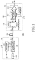
- FIG 1 shows, by way of illustrative and non-limitative example, the construction of an NRZ (non-return-to-zero) differential polarization shift-keying optical transmission system according to a first preferred embodiment of the present invention.
- the optical transmission system 100 includes a transmitter unit (TX) 110 and a receiver unit (RX) 160, which are connected to each other by an optical fiber 150.
- the transmitter unit 110 includes a light source (LS) 120, a precoder 130, and a polarization modulator 140.
- the receiver unit 160 includes a 1-bit delay interferometer 170 and a balanced receiver 210.
- the balanced receiver 210 includes first and second optical detectors 212, 214 and a differential amplifier 216.
- Each of the first and second optical detectors 212, 214 includes a photodiode (PD), which is a conventional photoelectric element.
- the differential amplifier 216 includes an output terminal, a (-) input terminal connected with the first optical detector 212, and a (+) input terminal connected with the second optical detector 214.
- the light source 120 of the transmitter unit 110 outputs CW-mode light and includes a conventional CW laser diode.
- the precoder 130 is adapted to precode inputted data S1, shown in FIG 3, to generate a precoded electrical signal S2 and includes a 1-bit delay line 134 and an EXOR (exclusive OR) circuit 132.
- the precoder 130 may be constructed in various ways as long as it performs a precoding function.
- the precoder may be composed of a binary counter and a delay line. The binary counter counts inputted clock signals when inputted data has a predetermined value ('0' or '1') and outputs the result.
- the data S1 is given as, for example, '101010011000110'.
- the polarization modulator 140 uses the precoded electrical signal S2 to modulate, through polarization modulation, the light from the light source 120 and outputs a polarization-modulated optical signal S3.
- each '1' bit and '0' bit After being subject to the polarization modulation, each '1' bit and '0' bit have polarization modes (TE and TM modes) which are perpendicular to each other (that is, the angle between them is 90°).
- TE and TM modes polarization modes
- a '1' bit from the precoded electrical signal S2 has a TE mode component only and a '0' bit from the same has a TM mode component only.
- FIG 4 shows the construction of the 1-bit delay interferometer 170 and FIG 5 shows respective signals S4-S9 according to their position within the receiver unit 160.
- the receiver unit 160 is described below with reference to FIGs. 1, 4, and 5.
- the 1-bit delay interferometer 170 includes a beam splitter (BS) 180, first and second delay lines 192 and 194, and an optical coupler (OC) 200.
- BS beam splitter
- OC optical coupler
- the beam splitter 180 has a first input port 182 and first and second output ports 184, 186.
- the first input port 182 is connected with the optical fiber 150.
- the beam splitter 180 splits the polarization-modulated optical signal S3, which is inputted to the first input port 182, into first and second split optical signals through intensity split.
- the first and second split optical signals are outputted via the first and second output ports 184, 186, respectively.
- the optical coupler 200 has first and second input ports 202, 204 and first and second output ports 206, 208.
- the first input port 202 of the optical coupler 200 is connected with the first output port 184 of the beam splitter 180 via the first delay line 192 and the second input port 204 of the coupler is connected with the second output port 186 of the beam splitter 180 via the second delay line 194.
- the second delay line 194 is longer than the first delay line 192 by a length which corresponds to 1 bit.
- the second split optical signal hereinafter, referred to as a "delayed optical signal" S4 is delayed by 1 bit more than the first split optical signal S3, which has passed through the first delay line 192.
- the optical coupler 200 inverts the phase of a part of the first split optical signal S3, which is inputted to the second input port 202 of the coupler, to generate a phase-inverted optical signal.
- the optical coupler 200 causes a part of the delayed optical signal S4 to interfere with another part of the first split optical signal S3 and generate a constructive-interferential optical signal S5, which is outputted via the first output port 206 of the optical coupler.
- bits which have the same polarization and the same phase relative to the first split optical signal S3 and the delayed optical signal S4 are outputted as constructive-interferential bits and, on the other hand, bits which have orthogonal polarization but the same phase are outputted as bits whose polarization is slanted 45° relative to a TE mode axis.
- the optical coupler 200 causes another part of the delayed optical signal S4 to interfere with the phase-inverted optical signal and generate a destructive-interferential optical signal S6, which is outputted via the second output port 208 of the coupler.
- the destructive-interferential optical signal S6 on one hand, bits which have the same polarization and the same phase relative to the first split optical signal S3 and the delayed optical signal S4 undergo destructive interference with one another and are outputted as extinct bits ('0' bits) and, on the other hand, bits which have orthogonal polarization but the same phase are outputted as bits whose polarization is slanted 135° relative to a TE mode axis.
- the first optical detector 212 is connected with the first output port 206 of the optical coupler 200 and is adapted to output a first detection signal S7, which is obtained through photoelectric conversion of the constructive-interferential optical signal S5 inputted from the first output port of the coupler.
- the second optical detector 214 is connected with the second output port 208 of the optical coupler 200 and is adapted to output a second detection signal S8, which is obtained through photoelectric conversion of the destructive-interferential optical signal S6 inputted from the second output port of the coupler.
- the differential amplifier 216 outputs, via the output terminal, a differential signal S9 corresponding to a difference between the first and second detection signals S7, S8, which are inputted to the (-) and (+) input terminals, respectively.
- a comparison of FIGs. 3 and 5 shoes that the differential signal S9 outputted from the receiver 160 is equal to the data S 1 inputted to the transmitter 110.
- FIG 6 shows one example of a construction of an RZ (return-to-zero) differential polarization shift-keying optical transmission system according to a second preferred embodiment of the present invention.
- the optical transmission system 300 is identical to the optical transmission system 100 shown in FIG 1, except that the precoder 130 is removed and an auxiliary optical modulator 340 is added for RZ coding. Therefore, repeated descriptions of the same components, except the auxiliary optical modulator 340, are omitted.
- the optical transmission system 300 includes a transmitter unit 310 and a receiver unit 360, which are connected to each other by an optical fiber 350.
- the transmitter unit 310 includes a light source 320; a polarization modulator 330 adapted to receive, as input, data and CW-mode light from the light source; and the auxiliary optical modulator 340.
- the receiver unit 360 includes a 1-bit delay interferometer 370 and a balanced receiver 380.
- the balanced receiver 380 has first and second optical detectors 382, 384 and a differential amplifier 3 86.
- the auxiliary optical modulator 340 generates an optical pulse stream, which corresponds to a clock frequency, using an inputted clock signal or a half-frequency signal of a clock.
- a polarization-modulated optical signal which is inputted from the polarization modulator 330, is loaded into the optical pulse stream and is transmitted via the optical fiber 350.
- an RZ mode has a reception sensitivity which is improved by about 2 dB, compared with an NRZ mode, and is advantageous in that the transmission length of the optical transmission system 300 can be extended or a margin of the optical transmission system 300 can be assured.
- FIG 7 shows an exemplary construction of an RZ (return-to-zero) differential polarization shift-keying optical transmission system according to a third preferred embodiment of the present invention.
- the optical transmission system 400 is identical to the optical transmission system 300 shown in FIG 6, except that the serial order of arrangement of a polarization modulator 440 and an auxiliary optical modulator 430 is reverse to that of the counterpart components in FIG 6. Therefore, repeated descriptions of the same components will be omitted.
- the optical transmission system 400 includes a transmitter unit 410 and a receiver unit 460, which are connected to each other by an optical fiber 450.
- the transmitter unit 410 includes a light source 420, the auxiliary optical modulator 430, and the polarization modulator 440 adapted to receive, as input, data and an optical pulse stream from the auxiliary optical modulator 430.
- the receiver unit 460 includes a 1-bit delay interferometer 470 and a balanced receiver 480.
- the balanced receiver 480 has first and second optical detectors 482, 484 and a differential amplifier 486.
- the light source 420 outputs CW-mode light.
- the auxiliary optical modulator 430 uses an inputted clock signal or a half-frequency signal of a clock to generate, from the CW-mode light, an optical pulse stream which corresponds to a clock frequency.
- the polarization modulator 440 modulates the optical pulse stream through polarization modulation and generates a polarization-modulated optical signal, which is then transmitted via the optical fiber 450.
- a differential polarization shift-keying optical transmission system uses a polarization modulation mode to implement a receiver unit that is composed of a 1-bit delay interferometer and a balanced receiver.
- the resulting device affords superior reception sensitivity and is less subject to the Kerr nonlinear effect of optical fibers.
- the need is eliminated for any additional active controller device.
- a long-distance optical transmission system can therefore be realized at a substantially reduced cost, and with remarkably improved system performance.
Landscapes
- Physics & Mathematics (AREA)
- Electromagnetism (AREA)
- Engineering & Computer Science (AREA)
- Computer Networks & Wireless Communication (AREA)
- Signal Processing (AREA)
- General Physics & Mathematics (AREA)
- Optics & Photonics (AREA)
- Optical Communication System (AREA)
Abstract
Description
Claims (20)
- A differential polarization shift-keying optical transmission system comprising:a transmitter unit configured to precode inputted data to form a precoded signal and to use the precoded signal to generate and output a polarization-modulated optical signal; anda receiver unit connected with the transmitter unit via an optical fiber for optical transmission, said receiver unit including:a delay interferometer configured to split the optical signal from the transmitter unit into first and second split optical signals, generate a delayed optical signal by causing the second split optical signal to be delayed, generate a phase-inverted optical signal by inverting the phase of a part of the first split optical signal, generate a constructive-interferential optical signal by causing a part of the delayed optical signal to interfere with another part of the first split optical signal, and generate a destructive-interferential optical signal by causing another part of the delayed optical signal to interfere with the phase-inverted optical signal; anda balanced receiver configured to output a differential signal between the constructive-interferential optical signal and the destructive-interferential optical signal.
- The differential polarization shift-keying optical transmission system as claimed in claim 1, wherein the transmitter unit includes:a light source configured to output CW-mode light;a precoder configured to perform the precoding of the inputted data, said precoded signal being a precoded electrical signal; anda polarization modulator configured to use the precoded signal to modulate, through polarization modulation, the light from the light source in performing the generating and outputting of the polarization-modulated optical signal.
- The differential polarization shift-keying optical transmission system as claimed in claim 1 or 2, wherein the transmitter unit includes:a light source configured to output CW-mode light;a polarization modulator configured to use the inputted data to modulate, through polarization modulation, the light from the light source in performing the generating and outputting of the polarization-modulated optical signal; andan auxiliary optical modulator configured to generate an optical pulse stream which has a frequency, load into the optical pulse stream the outputted polarization-modulated optical signal, and transmit the optical pulse stream via the optical fiber.
- The differential polarization shift-keying optical transmission system as claimed in one of claims 1 to 3, wherein the transmitter unit includes:a light source configured to generate CW-mode light;an auxiliary optical modulator configured to generate from the CW-mode light an optical pulse stream, which has a frequency; anda polarization modulator configured to use the inputted data to modulate, through polarization modulation, the optical pulse stream in performing the generating and outputting of the polarization-modulated optical signal, said outputting occurring via the optical fiber.
- The differential polarization shift-keying optical transmission system as claimed in one of claims 1 to 4, wherein the delay interferometer is a 1-bit delay interferometer.
- The differential polarization shift-keying optical transmission system as claimed in claim 5, wherein the 1-bit delay interferometer includes a beam splitter configured to perform the split, through intensity split, and output said first and second split optical signals via first and second output ports of the beam splitter, said optical signal being inputted to a first input port of the beam splitter, said first input port being in optical connection with the optical fiber.
- The differential polarization shift-keying optical transmission system as claimed in claim 6, wherein the 1-bit delay interferometer further includes first and second delay lines which are in connection with the first and second output ports, respectively, and are configured to generate said delayed optical signal by causing the second split optical signal to be more delayed than the first split optical signal by 1 bit.
- The differential polarization shift-keying optical transmission system as claimed in claim 7, wherein the 1-bit delay interferometer further includes an optical coupler configured for the generating of the phase-inverted, constructive-interferential and destructive-interferential optical signals, said first split optical signal being inputted to an input port of the optical coupler, said input port of the optical coupler being in connection with the first delay line, said constructive-interferential and destructive-interferential optical signals being outputted, respectively, via first and second output ports of the optical coupler.
- The differential polarization shift-keying optical transmission system as claimed in claim 8, wherein the balanced receiver includes a first optical detector which is in optical connection with the first output port of the optical coupler and is configured to output a first detection signal, which is obtained through photoelectric conversion of the constructive-interferential optical signal.
- The differential polarization shift-keying optical transmission system as claimed in claim 9, wherein the balanced receiver further includes a second optical detector which is in optical connection with the second output port of the optical coupler and is configured to output a second detection signal, which is obtained through photoelectric conversion of the destructive-interferential optical signal.
- The differential polarization shift-keying optical transmission system as claimed in claim 10, wherein the balanced receiver further includes a differential amplifier which includes a (-) input terminal connected with the first optical detector, a (+) input terminal connected with the second optical detector, and an output terminal and is configured to output, via the output terminal, the differential signal corresponding to a difference between the first and second detection signals, which are inputted to the (-) and (+) input terminals, respectively.
- A transmitter unit configured to precode inputted data to form a precoded signal and to use the precoded signal to generate and output a polarization-modulated optical signal.
- The transmitter unit of claim 12, said transmitter unit comprising:a light source configured to output CW-mode light;a precoder configured to perform the precoding of the inputted data, said precoded signal being a precoded electrical signal; anda polarization modulator configured to use the precoded signal to modulate, through polarization modulation, the light from the light source in performing the generating and outputting of the polarization-modulated optical signal.
- The transmitter unit of claim 12 or 13, said transmitter unit comprising:a light source configured to output CW-mode light;a polarization modulator configured to use the inputted data to modulate, through polarization modulation, the light from the light source in performing the generating and outputting of the polarization-modulated optical signal; andan auxiliary optical modulator configured to generate an optical pulse stream which has a frequency, load into the optical pulse stream the outputted polarization-modulated optical signal, and transmit the optical pulse stream via an optical fiber.
- The transmitter unit of one of claims 12 to 14, said transmitter unit comprising:a light source configured to generate CW-mode light;an auxiliary optical modulator configured to generate from the CW-mode light an optical pulse stream, which has a frequency; anda polarization modulator configured to use the inputted data to modulate, through polarization modulation, the optical pulse stream in performing the generating and outputting of the polarization-modulated optical signal, said outputting occurring via an optical fiber.
- A receiver unit comprising:a 1-bit delay interferometer configured to split an optical signal into first and second split optical signals, generate a delayed optical signal by causing the second split optical signal to be delayed, generate a phase-inverted optical signal by inverting the phase of a part of the first split optical signal, generate a constructive-interferential optical signal by causing a part of the delayed optical signal to interfere with another part of the first split optical signal, and generate a destructive-interferential optical signal by causing another part of the delayed optical signal to interfere with the phase-inverted optical signal; anda balanced receiver configured to output a differential signal between the constructive-interferential optical signal and the destructive-interferential optical signal.
- The receiver unit of claim 16, wherein the 1-bit delay interferometer includes a beam splitter configured to perform the split, through intensity split, and output said first and second split optical signals via first and second output ports of the beam splitter, said optical signal being inputted to a first input port of the beam splitter, said first input port being in optical connection with an optical fiber.
- The receiver unit of claim 17, wherein the 1-bit delay interferometer further includes first and second delay lines which are in connection with the first and second output ports, respectively, and are configured to generate said delayed optical signal by causing the second split optical signal to be more delayed than the first split optical signal by 1 bit.
- The receiver unit of claim 18, wherein the 1-bit delay interferometer further includes an optical coupler configured for the generating of the phase-inverted, constructive-interferential and destructive-interferential optical signals, said first split optical signal being inputted to an input port of the optical coupler, said input port of the optical coupler being in connection with the first delay line, said constructive-interferential and destructive-interferential optical signals being outputted, respectively, via first and second output ports of the optical coupler.
- The receiver unit of claim 19, wherein the balanced receiver includes a first optical detector which is in optical connection with the first output port of the optical coupler and is configured to output a first detection signal, which is obtained through photoelectric conversion of the constructive-interferential optical signal; a second optical detector which is in optical connection with the second output port of the optical coupler and is configured to output a second detection signal, which is obtained through photoelectric conversion of the destructive-interferential optical signal; and a differential amplifier which includes a (-) input terminal connected with the first optical detector, a (+) input terminal connected with the second optical detector, and an output terminal and is configured to output, via the output terminal, the differential signal corresponding to a difference between the first and second detection signals, which are inputted to the (-) and (+) input terminals, respectively.
Applications Claiming Priority (2)
| Application Number | Priority Date | Filing Date | Title |
|---|---|---|---|
| KR2003084041 | 2003-11-25 | ||
| KR1020030084041A KR100584433B1 (en) | 2003-11-25 | 2003-11-25 | Differential Polarization Modulation Optical Transmission System |
Publications (3)
| Publication Number | Publication Date |
|---|---|
| EP1536578A2 true EP1536578A2 (en) | 2005-06-01 |
| EP1536578A3 EP1536578A3 (en) | 2005-11-02 |
| EP1536578B1 EP1536578B1 (en) | 2007-03-14 |
Family
ID=34464740
Family Applications (1)
| Application Number | Title | Priority Date | Filing Date |
|---|---|---|---|
| EP04027100A Expired - Lifetime EP1536578B1 (en) | 2003-11-25 | 2004-11-15 | Differential polarization shift-keying optical transmission system |
Country Status (6)
| Country | Link |
|---|---|
| US (1) | US20050111851A1 (en) |
| EP (1) | EP1536578B1 (en) |
| JP (1) | JP2005160065A (en) |
| KR (1) | KR100584433B1 (en) |
| CN (1) | CN100374910C (en) |
| DE (1) | DE602004005290T2 (en) |
Cited By (2)
| Publication number | Priority date | Publication date | Assignee | Title |
|---|---|---|---|---|
| WO2008125848A1 (en) * | 2007-04-12 | 2008-10-23 | Uws Ventures Limited | A receiver |
| RU2761760C1 (en) * | 2021-03-05 | 2021-12-13 | Валерий Константинович Любезнов | Method and device for receiving and detecting an optical manipulated scanning signal of a given area |
Families Citing this family (18)
| Publication number | Priority date | Publication date | Assignee | Title |
|---|---|---|---|---|
| KR100594072B1 (en) * | 2004-10-06 | 2006-06-30 | 삼성전자주식회사 | Differential Phase Modulated and Frequency Modulated Optical Signal Receivers |
| GB2428149B (en) * | 2005-07-07 | 2009-10-28 | Agilent Technologies Inc | Multimode optical fibre communication system |
| US8503881B1 (en) * | 2007-04-06 | 2013-08-06 | University Of Central Florida Research Foundation, Inc. | Systems for extending WDM transmission into the O-band |
| KR100860549B1 (en) * | 2007-06-25 | 2008-09-26 | 광주과학기술원 | Optical Signal Processing System and Method Using Polarization Modulation Phenomenon |
| US9019087B2 (en) * | 2007-10-16 | 2015-04-28 | Immersion Corporation | Synchronization of haptic effect data in a media stream |
| EP2206306B1 (en) * | 2007-10-16 | 2017-03-29 | Oclaro Subsystems, Inc. | Balanced phase-shaped binary transmission in optical communications |
| CN101170363B (en) * | 2007-10-26 | 2010-12-08 | 中兴通讯股份有限公司 | An Optical Differential Polarization Shift Keying System and Its Signal Sending Device and Method |
| CN101860500B (en) | 2009-04-13 | 2013-10-09 | 华为技术有限公司 | Methods, devices and systems for generating and receiving phase polarization modulation signals |
| KR101382619B1 (en) * | 2009-07-24 | 2014-04-07 | 한국전자통신연구원 | Apparatus and method for optical transmitting, and apparatus and method for optical receiving |
| GB201002963D0 (en) * | 2010-02-22 | 2010-04-07 | Uws Ventures Ltd | A communication system |
| CN101795159B (en) * | 2010-03-26 | 2012-09-26 | 武汉邮电科学研究院 | High-speed WDM (Wavelength Division Multiplexing) light communication system and method for resisting non-linearity effect in same |
| KR101347294B1 (en) * | 2010-07-21 | 2014-01-03 | 한국전자통신연구원 | Optical receiving apparatus and method for controlling phase offset for differential quadrature phase shift keying |
| JP5675219B2 (en) * | 2010-08-27 | 2015-02-25 | キヤノン株式会社 | Optical pulse generator, terahertz spectrometer and tomography device |
| CN104180831A (en) * | 2013-05-24 | 2014-12-03 | 无锡万润光子技术有限公司 | Sensitivity-enhanced optical time domain reflection distributed Michelson interferometer based on two-core optical fiber |
| CN103743674A (en) * | 2013-09-30 | 2014-04-23 | 北京航空航天大学 | Method and system for enhancing non-specular reflection effect |
| US10333627B2 (en) * | 2017-06-26 | 2019-06-25 | Inphi Corporation | Rx delay line inteferometer tracking in closed-loop module control for communication |
| CN111555863B (en) * | 2019-02-12 | 2022-04-29 | 科大国盾量子技术股份有限公司 | Sending end, encoding method and quantum key distribution system for time phase-polarization combined encoding |
| CN112113515B (en) * | 2020-10-14 | 2022-03-11 | 福建师范大学 | Phase encoding and phase decoding method and device for single interferometric reading phase |
Family Cites Families (16)
| Publication number | Priority date | Publication date | Assignee | Title |
|---|---|---|---|---|
| US4352071A (en) * | 1979-06-22 | 1982-09-28 | Communications Satellite Corporation | Planar QPSK demodulator |
| IT1238535B (en) * | 1989-11-14 | 1993-08-18 | Cselt Centro Studi Lab Telecom | COHERENT COMMUNICATION SYSTEM IN OPTICAL FIBER WITH DIFFERENT POLARIZATION IN TRANSMISSION |
| WO1995007584A1 (en) * | 1993-09-09 | 1995-03-16 | British Telecommunications Public Limited Company | System and method for quantum cryptography |
| GB2334641A (en) * | 1998-02-11 | 1999-08-25 | Northern Telecom Ltd | Multiplexed transmission of optical signals |
| JP3173591B2 (en) * | 1998-06-09 | 2001-06-04 | 日本電気株式会社 | Optical transmitter, optical transmission system and signal light modulation method |
| GB9818941D0 (en) * | 1998-08-28 | 1998-10-21 | Northern Telecom Ltd | Polarisation mode dispersion compensation |
| GB9820493D0 (en) * | 1998-09-22 | 1998-11-11 | Secr Defence | Optical phase detector |
| US6626589B1 (en) * | 1999-12-29 | 2003-09-30 | Nortel Networks Limited | Optical packet switching |
| US6522462B2 (en) * | 2001-06-29 | 2003-02-18 | Super Light Wave Corp. | All optical logic using cross-phase modulation amplifiers and mach-zehnder interferometers with phase-shift devices |
| US6643063B2 (en) * | 2001-11-14 | 2003-11-04 | Oplink Communications, Inc. | Deinterleaver with high isolation and dispersion compensation and 50/200GHz interleaver and deinterleaver |
| US7277647B2 (en) * | 2002-03-14 | 2007-10-02 | Lucent Technologies Inc. | System and method of optical transmission |
| JP2003307717A (en) * | 2002-04-17 | 2003-10-31 | Sumitomo Electric Ind Ltd | Optical signal processing device |
| US6760142B2 (en) * | 2002-05-13 | 2004-07-06 | Lucent Technologies Inc. | Delay interferometer optical pulse generator |
| US7260330B2 (en) * | 2002-11-04 | 2007-08-21 | The Boeing Company | Optical communication system using correlation receiver |
| JP4554519B2 (en) * | 2003-08-27 | 2010-09-29 | 三菱電機株式会社 | Optical transmitter |
| US20050069330A1 (en) * | 2003-09-29 | 2005-03-31 | Yuan-Hua Kao | System and method for optical transmission |
-
2003
- 2003-11-25 KR KR1020030084041A patent/KR100584433B1/en not_active Expired - Fee Related
-
2004
- 2004-07-28 US US10/901,277 patent/US20050111851A1/en not_active Abandoned
- 2004-09-28 CN CNB2004100120353A patent/CN100374910C/en not_active Expired - Fee Related
- 2004-11-11 JP JP2004327916A patent/JP2005160065A/en active Pending
- 2004-11-15 DE DE602004005290T patent/DE602004005290T2/en not_active Expired - Fee Related
- 2004-11-15 EP EP04027100A patent/EP1536578B1/en not_active Expired - Lifetime
Cited By (2)
| Publication number | Priority date | Publication date | Assignee | Title |
|---|---|---|---|---|
| WO2008125848A1 (en) * | 2007-04-12 | 2008-10-23 | Uws Ventures Limited | A receiver |
| RU2761760C1 (en) * | 2021-03-05 | 2021-12-13 | Валерий Константинович Любезнов | Method and device for receiving and detecting an optical manipulated scanning signal of a given area |
Also Published As
| Publication number | Publication date |
|---|---|
| CN1621874A (en) | 2005-06-01 |
| EP1536578B1 (en) | 2007-03-14 |
| DE602004005290T2 (en) | 2007-06-28 |
| JP2005160065A (en) | 2005-06-16 |
| KR20050050332A (en) | 2005-05-31 |
| DE602004005290D1 (en) | 2007-04-26 |
| CN100374910C (en) | 2008-03-12 |
| KR100584433B1 (en) | 2006-05-26 |
| EP1536578A3 (en) | 2005-11-02 |
| US20050111851A1 (en) | 2005-05-26 |
Similar Documents
| Publication | Publication Date | Title |
|---|---|---|
| EP1536578A2 (en) | Differential polarization shift-keying optical transmission system | |
| Yonenaga et al. | Dispersion-tolerant optical transmission system using duobinary transmitter and binary receiver | |
| US11606144B2 (en) | Pluggable optical module and optical communication system | |
| US11245474B2 (en) | Pluggable optical module and optical communication system | |
| JP3721062B2 (en) | Optical transmitter | |
| CA2588585C (en) | Method and apparatus for bias and alignment control in an optical signal transmitter | |
| US20100189437A1 (en) | Optical receiver and optical reception method compatible with differential quadrature phase shift keying | |
| US20120121264A1 (en) | Apparatus and method for transmitting light, and apparatus and method for receiving light | |
| JP2011530885A (en) | Frequency offset polarization multiplexed modulation format and system incorporating the same | |
| KR100703410B1 (en) | Offset Quadrature Phase Shift Keying Method and Optical Transmitter | |
| GB2354598A (en) | An optical modulator | |
| KR100594155B1 (en) | Dual Binary Optical Transmitter Resistant to Color Dispersion | |
| CN101170363B (en) | An Optical Differential Polarization Shift Keying System and Its Signal Sending Device and Method | |
| US9325423B1 (en) | Systems and methods for complementary signal transmission | |
| JP2004364288A (en) | System and method for alternate mark inversion and duobinary optical transmission | |
| CN113708844B (en) | Polarization controller and polarization control method | |
| US7483640B2 (en) | Optical multilevel-coded signal transmission system and method thereof, optical transmitter, and multilevel-coded signal light generating method | |
| US10425166B2 (en) | Optical transmitter, optical transmission apparatus, and optical modulation method | |
| US6728490B1 (en) | Optical transmitter, optical receiver, optical transmission system, and optical transmission method | |
| JP5424939B2 (en) | Optical phase noise suppression circuit, phase fluctuation detection circuit, and phase fluctuation detection method | |
| JP4028463B2 (en) | Optical transmitter and optical transmitter / receiver | |
| Kang et al. | 1650-km transmission of 50-Gb/s NRZ and RZ-DQPSK signals generated using an electroabsorption modulators-silica planar lightwave circuit hybrid integrated device | |
| KR100559138B1 (en) | Optical communication system and its modulation and transmission method | |
| JP2011182197A (en) | Optical noise reduction circuit, and optical noise reduction method | |
| JP2010062654A (en) | Optical transmission apparatus and light transmission system |
Legal Events
| Date | Code | Title | Description |
|---|---|---|---|
| PUAI | Public reference made under article 153(3) epc to a published international application that has entered the european phase |
Free format text: ORIGINAL CODE: 0009012 |
|
| 17P | Request for examination filed |
Effective date: 20041115 |
|
| AK | Designated contracting states |
Kind code of ref document: A2 Designated state(s): AT BE BG CH CY CZ DE DK EE ES FI FR GB GR HU IE IS IT LI LU MC NL PL PT RO SE SI SK TR |
|
| AX | Request for extension of the european patent |
Extension state: AL HR LT LV MK YU |
|
| PUAL | Search report despatched |
Free format text: ORIGINAL CODE: 0009013 |
|
| AK | Designated contracting states |
Kind code of ref document: A3 Designated state(s): AT BE BG CH CY CZ DE DK EE ES FI FR GB GR HU IE IS IT LI LU MC NL PL PT RO SE SI SK TR |
|
| AX | Request for extension of the european patent |
Extension state: AL HR LT LV MK YU |
|
| AKX | Designation fees paid |
Designated state(s): DE FR GB |
|
| GRAP | Despatch of communication of intention to grant a patent |
Free format text: ORIGINAL CODE: EPIDOSNIGR1 |
|
| RAP1 | Party data changed (applicant data changed or rights of an application transferred) |
Owner name: SAMSUNG ELECTRONICS CO., LTD. |
|
| GRAS | Grant fee paid |
Free format text: ORIGINAL CODE: EPIDOSNIGR3 |
|
| GRAA | (expected) grant |
Free format text: ORIGINAL CODE: 0009210 |
|
| AK | Designated contracting states |
Kind code of ref document: B1 Designated state(s): DE FR GB |
|
| REG | Reference to a national code |
Ref country code: GB Ref legal event code: FG4D |
|
| REF | Corresponds to: |
Ref document number: 602004005290 Country of ref document: DE Date of ref document: 20070426 Kind code of ref document: P |
|
| ET | Fr: translation filed | ||
| PLBE | No opposition filed within time limit |
Free format text: ORIGINAL CODE: 0009261 |
|
| STAA | Information on the status of an ep patent application or granted ep patent |
Free format text: STATUS: NO OPPOSITION FILED WITHIN TIME LIMIT |
|
| 26N | No opposition filed |
Effective date: 20071217 |
|
| PGFP | Annual fee paid to national office [announced via postgrant information from national office to epo] |
Ref country code: DE Payment date: 20081114 Year of fee payment: 5 |
|
| PGFP | Annual fee paid to national office [announced via postgrant information from national office to epo] |
Ref country code: FR Payment date: 20081112 Year of fee payment: 5 |
|
| PGFP | Annual fee paid to national office [announced via postgrant information from national office to epo] |
Ref country code: GB Payment date: 20081112 Year of fee payment: 5 |
|
| GBPC | Gb: european patent ceased through non-payment of renewal fee |
Effective date: 20091115 |
|
| REG | Reference to a national code |
Ref country code: FR Ref legal event code: ST Effective date: 20100730 |
|
| PG25 | Lapsed in a contracting state [announced via postgrant information from national office to epo] |
Ref country code: FR Free format text: LAPSE BECAUSE OF NON-PAYMENT OF DUE FEES Effective date: 20091130 |
|
| PG25 | Lapsed in a contracting state [announced via postgrant information from national office to epo] |
Ref country code: DE Free format text: LAPSE BECAUSE OF NON-PAYMENT OF DUE FEES Effective date: 20100601 |
|
| PG25 | Lapsed in a contracting state [announced via postgrant information from national office to epo] |
Ref country code: GB Free format text: LAPSE BECAUSE OF NON-PAYMENT OF DUE FEES Effective date: 20091115 |