EP1536524A1 - Connector - Google Patents
Connector Download PDFInfo
- Publication number
- EP1536524A1 EP1536524A1 EP03794099A EP03794099A EP1536524A1 EP 1536524 A1 EP1536524 A1 EP 1536524A1 EP 03794099 A EP03794099 A EP 03794099A EP 03794099 A EP03794099 A EP 03794099A EP 1536524 A1 EP1536524 A1 EP 1536524A1
- Authority
- EP
- European Patent Office
- Prior art keywords
- contact
- contact members
- points
- connector
- rows
- Prior art date
- Legal status (The legal status is an assumption and is not a legal conclusion. Google has not performed a legal analysis and makes no representation as to the accuracy of the status listed.)
- Withdrawn
Links
Images




Classifications
-
- H—ELECTRICITY
- H01—ELECTRIC ELEMENTS
- H01R—ELECTRICALLY-CONDUCTIVE CONNECTIONS; STRUCTURAL ASSOCIATIONS OF A PLURALITY OF MUTUALLY-INSULATED ELECTRICAL CONNECTING ELEMENTS; COUPLING DEVICES; CURRENT COLLECTORS
- H01R12/00—Structural associations of a plurality of mutually-insulated electrical connecting elements, specially adapted for printed circuits, e.g. printed circuit boards [PCB], flat or ribbon cables, or like generally planar structures, e.g. terminal strips, terminal blocks; Coupling devices specially adapted for printed circuits, flat or ribbon cables, or like generally planar structures; Terminals specially adapted for contact with, or insertion into, printed circuits, flat or ribbon cables, or like generally planar structures
- H01R12/50—Fixed connections
- H01R12/51—Fixed connections for rigid printed circuits or like structures
- H01R12/55—Fixed connections for rigid printed circuits or like structures characterised by the terminals
- H01R12/58—Fixed connections for rigid printed circuits or like structures characterised by the terminals terminals for insertion into holes
-
- H—ELECTRICITY
- H01—ELECTRIC ELEMENTS
- H01R—ELECTRICALLY-CONDUCTIVE CONNECTIONS; STRUCTURAL ASSOCIATIONS OF A PLURALITY OF MUTUALLY-INSULATED ELECTRICAL CONNECTING ELEMENTS; COUPLING DEVICES; CURRENT COLLECTORS
- H01R13/00—Details of coupling devices of the kinds covered by groups H01R12/70 or H01R24/00 - H01R33/00
- H01R13/02—Contact members
- H01R13/22—Contacts for co-operating by abutting
- H01R13/24—Contacts for co-operating by abutting resilient; resiliently-mounted
- H01R13/2435—Contacts for co-operating by abutting resilient; resiliently-mounted with opposite contact points, e.g. C beam
-
- H—ELECTRICITY
- H01—ELECTRIC ELEMENTS
- H01R—ELECTRICALLY-CONDUCTIVE CONNECTIONS; STRUCTURAL ASSOCIATIONS OF A PLURALITY OF MUTUALLY-INSULATED ELECTRICAL CONNECTING ELEMENTS; COUPLING DEVICES; CURRENT COLLECTORS
- H01R12/00—Structural associations of a plurality of mutually-insulated electrical connecting elements, specially adapted for printed circuits, e.g. printed circuit boards [PCB], flat or ribbon cables, or like generally planar structures, e.g. terminal strips, terminal blocks; Coupling devices specially adapted for printed circuits, flat or ribbon cables, or like generally planar structures; Terminals specially adapted for contact with, or insertion into, printed circuits, flat or ribbon cables, or like generally planar structures
- H01R12/70—Coupling devices
- H01R12/71—Coupling devices for rigid printing circuits or like structures
- H01R12/712—Coupling devices for rigid printing circuits or like structures co-operating with the surface of the printed circuit or with a coupling device exclusively provided on the surface of the printed circuit
- H01R12/714—Coupling devices for rigid printing circuits or like structures co-operating with the surface of the printed circuit or with a coupling device exclusively provided on the surface of the printed circuit with contacts abutting directly the printed circuit; Button contacts therefore provided on the printed circuit
-
- H—ELECTRICITY
- H01—ELECTRIC ELEMENTS
- H01R—ELECTRICALLY-CONDUCTIVE CONNECTIONS; STRUCTURAL ASSOCIATIONS OF A PLURALITY OF MUTUALLY-INSULATED ELECTRICAL CONNECTING ELEMENTS; COUPLING DEVICES; CURRENT COLLECTORS
- H01R12/00—Structural associations of a plurality of mutually-insulated electrical connecting elements, specially adapted for printed circuits, e.g. printed circuit boards [PCB], flat or ribbon cables, or like generally planar structures, e.g. terminal strips, terminal blocks; Coupling devices specially adapted for printed circuits, flat or ribbon cables, or like generally planar structures; Terminals specially adapted for contact with, or insertion into, printed circuits, flat or ribbon cables, or like generally planar structures
- H01R12/70—Coupling devices
- H01R12/71—Coupling devices for rigid printing circuits or like structures
- H01R12/72—Coupling devices for rigid printing circuits or like structures coupling with the edge of the rigid printed circuits or like structures
- H01R12/721—Coupling devices for rigid printing circuits or like structures coupling with the edge of the rigid printed circuits or like structures cooperating directly with the edge of the rigid printed circuits
-
- H—ELECTRICITY
- H01—ELECTRIC ELEMENTS
- H01R—ELECTRICALLY-CONDUCTIVE CONNECTIONS; STRUCTURAL ASSOCIATIONS OF A PLURALITY OF MUTUALLY-INSULATED ELECTRICAL CONNECTING ELEMENTS; COUPLING DEVICES; CURRENT COLLECTORS
- H01R12/00—Structural associations of a plurality of mutually-insulated electrical connecting elements, specially adapted for printed circuits, e.g. printed circuit boards [PCB], flat or ribbon cables, or like generally planar structures, e.g. terminal strips, terminal blocks; Coupling devices specially adapted for printed circuits, flat or ribbon cables, or like generally planar structures; Terminals specially adapted for contact with, or insertion into, printed circuits, flat or ribbon cables, or like generally planar structures
- H01R12/70—Coupling devices
- H01R12/77—Coupling devices for flexible printed circuits, flat or ribbon cables or like structures
- H01R12/79—Coupling devices for flexible printed circuits, flat or ribbon cables or like structures connecting to rigid printed circuits or like structures
Definitions
- the present invention relates to a connector for connecting printed circuit boards, flexible printed wiring boards (hereinafter abbreviated to FPC), or a printed circuit board and an FPC, for example.
- FPC flexible printed wiring boards
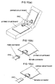
- the above connector is used, for example, in a bending part (hinged part) of a folding type cell phone for connecting printed circuit boards in an upper case and a lower case.
- a bending part hinged part
- a lower case a bending part (hinged part) of a folding type cell phone for connecting printed circuit boards in an upper case and a lower case.
- male connectors attached to the opposite ends of an FPC are inserted in female connectors with terminals thereof soldered to ends of the circuit boards in the respective cases (see Japanese Patent Publication "Kokai" No. 9-82439 (pages 4-6, Figs. 1-14), for example).
- electrodes formed at opposite ends of an FPC are inserted in female connectors with terminals thereof soldered to ends of the circuit boards in the respective cases (see Japanese Patent Publication "Kokai" No. 8-186628 (pages 3-4, Figs. 1-5), for example).
- Example 1 requires four connectors, with male and female put together
- Example 2 requires only two female connectors.
- a solder mounting step is required for attaching the connectors to the circuit boards in the cases.
- the present invention has made having regard to the state of the art noted above, and its object is to provide a connector for realizing compactness and space saving in time of increasing electrodes, a simplified element construction and solderless mounting.
- a connector according to the present invention has the following characteristic features.
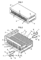
- a first characteristic feature of the present invention lies in comprising, as shown in Figs. 1 to 6, contact members 1 having elastically deformable points of contact formed in two locations, and a main connector body 2 for insulating and holding a plurality of contact members 1 arranged at intervals in a width direction with said points of contact A, B in the two locations of the respective contact members 1 being in the same positions as seen in the direction of arrangement, wherein said main connector body 2 includes a pair of socket portions 3 for receiving board ends 10 defining land electrodes 10a, 10b corresponding to said points of contact A, B of the respective contact members 1 lying in the same positions as seen in the direction of arrangement, so that the land electrodes 10a, 10b are in pressure contact with the corresponding points of contact A, B.
- the plurality of contact members having the elastically deformable points of contact formed in two locations are arranged at intervals in the direction of width.
- the board ends defining land electrodes corresponding to the points of contact of the respective contact members lying in the same positions as seen in the direction of arrangement are inserted, respectively, into the pair of socket portions of the main connector body which insulates and holds the contact members with the points of contact in the two locations being in the same positions as seen in the direction of arrangement. Then, the point of contacts of the contact members are pushed by the board ends to become elastically deformed, and the land electrodes formed on the board ends are placed in pressure contact with the corresponding points of contact of the contact members.
- the land electrodes formed on one of the board ends make a pressure contact with the points of contact in one of the two locations of the contact members, and the land electrodes formed on the other board end make a pressure contact with the points of contact in the other of the two locations of the contact members.
- the land electrodes of the above two board ends are conductively connected by the respective contact members.
- the main connector body insulates and holds the plurality of contact members arranged at intervals in the direction of width, and the two board ends to be connected are inserted into the main connector body to place the land electrodes of each board end in pressure contact with the points of contact in each end region of the contact members.
- This construction can achieve compactness and space saving by reducing the intervals at which the contact members are juxtaposed, despite an increase in the number of contact members for coping with multiple electrodes.
- the element construction is simple in that only the two elements, i.e. the contact members and the main connector body, are required, which achieves a reduction in die cost.
- the two board ends have only to be placed in pressure contact with the respective contact members, without requiring solder mounting, which eliminates the restriction as to the order of mounting the board ends.
- the flexibility of unit manufacture may be improved.
- a connector is provided for realizing compactness and space saving in time of increased electrodes, a simplified element construction and solderless mounting.
- a second characteristic feature of the present invention lies in that, in the first characteristic feature, as shown in Figs. 4 and 6, said contact members 1 are formed in an S-shape as seen in the direction of arrangement, and are held in a middle part of the S-shape by said main connector body 2, with said points of contact A, B being formed in end regions 1a, 1b of the S-shape extending in the same direction in which said board ends 10 are inserted for pressure contact.
- the contact members formed in an S-shape as seen in the direction of arrangement are held in a middle part of the S-shape by the main connector body, with the points of contact being formed in the end regions of the S-shape extending in the same direction in which the board ends are inserted for pressure contact therewith.
- the board ends are inserted, the end regions of the S-shaped contact members are pushed by the board ends, and the board ends can smoothly make a pressure contact with the point of contacts in the end regions of the S-shaped contact members.
- the end regions of the S-shaped contact members cease to be pushed by the board ends, and can smoothly return to the original state.
- a preferred embodiment of the connector which has a construction for hardly deforming the contact members in time of insertion or withdrawal of the board ends such as printed circuit boards or FPCs.
- a third characteristic feature of the present invention lies in that, in the first or second characteristic feature, the pair of socket portions 3 are formed in two opposite surfaces of the main connector body to receive said board ends 10 inserted in opposite directions.
- the two board ends are inserted in opposite directions into the pair of socket portions formed in the two opposite surfaces of the main connector body.
- the two board ends connected by the connector are arranged in the opposite sides of the connector to extend in the same direction without overlapping each other. This minimizes a mounting height and reduces a mounting space.
- a preferred embodiment of the connector which enables space saving in the connection and mounting of the boards using the connector.
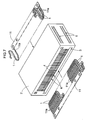
- a fourth characteristic feature of the present invention lies in that, in the first or second characteristic feature, as shown in Figs. 2 and 4, said main connector body 2 includes partition walls 4 for defining a plurality of divisions K for individually accommodating said contact members 1, and guides 5 for guiding said contact members 1 to be accommodated in said divisions K to positions to attain said arrangement; and said contact members 1 define guided portions 1c to be guided by said guides 5, and held portions 1d for press fitting with said partition walls 4 in time of guidance into said divisions K.
- the contact members are individually placed in the plurality of divisions defined by the partition walls in the main connector body, while guiding the guided portions formed on the contact members with the guides of the main connector body. Then, the contact members are guided to positions to attain said arrangement, and the held portions formed on the contact members press fit with, to be fixedly held by, the partition walls in time of guidance into the divisions.
- the contact members may be held in said arrangement in the main connector body.
- a preferred embodiment of the connector is provided for enabling assembly by a simple operation.
- a fifth characteristic feature of the present invention lies in that, in the first or second characteristic feature, as shown in Figs. 2 and 6, said contact members 1 are arranged in a plurality of rows with a gap in the directions of insertion of said board ends 10 into said socket portions 3.
- the contact members are arranged in a plurality of rows with a gap in the directions of insertion of said board ends into said socket portions.
- the board ends having the land electrodes formed in a plurality of rows and corresponding to the points of contact of the contact members are inserted into the respective socket portions, thereby establishing conduction between the land electrodes in the plurality of rows on the two board ends. That is, by arranging the contact members in a plurality of rows, while enlarging the intervals (pitch) at which the contact members are arranged in each row, an arrangement at a small pitch of the contact members is realized as the whole connector. This enables a connection of board ends having land electrodes formed with a narrow pitch.
- the greater number of electrodes results in the greater length of the connector in the direction of arrangement of the contact members.
- a preferred embodiment of the connector is provided which realizes compactness by minimizing the length of the connector despite an increase in the number of electrodes.
- a sixth characteristic feature of the present invention lies in that, in the fifth characteristic feature, as shown in Fig. 5, the positions of said points of contact A, B in the respective rows of said contact members 1 are staggered between the rows.
- the positions of the points of contact in the respective rows of the contact members are staggered between the rows, and the positions of the land electrodes on the board ends are also staggered between the rows in a corresponding relationship with the above.
- a preferred embodiment of the connector which can simplify circuit patterns on the board ends to be connected.
- a seventh characteristic feature of the present invention lies in that, in the fifth characteristic feature, as shown in Fig. 2, said points of contact A, B in the two locations are different in shape from each other, and are formed in positions of rotation symmetry through 180 degrees about the middle part of each of said contact members 1, said contact members 1 being arranged in two rows, with postures of the contact members 1 in the respective rows being reversed by 180 degrees between the rows.
- the contact members with said points of contact in the two locations different in shape from each other and formed in positions of rotation symmetry through 180 degrees about the middle part are arranged in two rows, with the postures of the contact members are reversed 180 degrees between the rows.
- the contact members of one type are arranged in the 180 degree posture reversal, whereby the points of contact located adjacent the inlets of the socket portions and the points of contact located in the depths have the same shapes.
- the contact members when elastically deformed by the board ends inserted into the respective socket portions, are displaced in the same state.
- a preferred embodiment of the connector which, while communizing the contact members, can maintain an excellent connection of the contact members to the board ends inserted in the respective socket portions.
- An eighth characteristic feature of the present invention lies in that, in the first or second characteristic feature, as shown in Figs. 2 and 6, said main connector body 2 includes retainers 6 for pressing on and holding said board ends 10 inserted in said socket portions 3.
- said board end inserted in the socket portions of said main connector body are pressed and held by the retainers provided in the main connector body, to prevent them from falling off the socket portions.
- a preferred embodiment of the connector which does not allow the board ends inserted in the connector to become detached with ease, thereby improving reliability in time of use.
- the connector according to this invention includes contact members 1 having elastically deformable points of contact A and B formed in two locations, and a main connector body 2 for insulating and holding a plurality of contact members 1 arranged at intervals in a width direction with the two points of contact A and B of the respective contact members 1 being in the same positions as seen in the direction of arrangement.
- Fig. 5 (b) is a cross section taken on line X-X shown in Fig. 5 (a)
- Fig. 6 is a view in vertical section taken on line Y-Y shown in Fig. 5 (a).
- the above main connector body 2 has a pair of socket portions 3 for receiving board ends 10 defining land electrodes 10a and 10b corresponding to the points of contact A and B of the respective contact members 1 lying in the same positions as seen in the direction of arrangement, so that the land electrodes 10a and 10b are in pressure contact with the corresponding points of contact A and B.
- the pair of socket portions 3 are formed in two opposite surfaces of the main connector body 2 to receive the board ends 10 inserted in opposite directions.
- the contact members 1 are formed in an S-shape as seen in the direction of arrangement, and are held in a middle part of the S-shape by the main connector body 2, with the points of contact A and B being formed in opposite end regions 1a and 1b of the S-shape extending in the same directions in which the board ends 10 are inserted for pressure contact.
- the contact members 1 are formed of a copper alloy, with the above points of contact A and B plated with gold.
- the main connector body 2 is formed of a plastic resin.
- the main connector body 2 has partition walls 4 for defining a plurality of divisions K of thin width for accommodating the plurality of contact members 1, respectively, and guides 5 for guiding the contact members 1 to be accommodated in the respective divisions K to the positions forming the state of arrangement.
- the guides 5 are formed of members integral with right and left partition walls 4 of the respective divisions K, and have upper surfaces 5a extending along the directions of insertion of the board ends 10, and receiving surfaces 5b at upstream ends in the directions of insertion.
- each S-shaped contact member 1 has guided portions 1c guided by the guides 4, and held portions 1d for press fitting with, to be fixedly held by, the partition walls 4 in time of guidance into the divisions K.
- each S-shaped contact member 1 has, formed in the middle region thereof, a linear portion of larger width than the other portions and narrower than the division K.
- the upper surface 1c of the linear middle portion acts as the guided portion 1c, and a pair of right and left tapered portions formed on side surfaces of the linear middle portion as staggered along the direction of insertion and protruding in obliquely sideways directions act as the held portions 1d.
- the contact members 1 are arranged in a plurality of rows with a gap in the directions of insertion of the board ends 10 into the socket portions 3.
- the positions of the points of contact A and B in the rows of the contact members 1 are staggered from one another between the rows.
- the contact members 1 are arranged in two rows, and the positions of the points of contact A and B are staggered by half (1/2 pitch) the pitch (e.g. 0.5mm) between the rows.
- the land electrodes 10a and 10b of the board ends 10 inserted are also formed in two rows, and the positions of the land electrodes 10a and 10b are staggered between the rows by 1/2 pitch.
- the two points of contact A and B of each contact member are different in shape, and are formed in positions of rotation symmetry through 180 degrees about the middle position of the contact member 1.
- the postures of the contact members 1 in the rows are reversed by 180 degrees between the rows.
- the inward land electrodes 10a of the board ends 10 contact the points of contact A of the contact members 1 located adjacent the inlets of the socket portions 3, and the outward land electrodes 10b of the board ends 10 contact the points of contact B of the contact members 1 located in the depths of the socket portions 3.
- the inward land electrodes 10a of one of the board ends 10 and the outward land electrodes 10b of the other board end 10 become conductive through the contact members 1.
- the two printed circuit boards having the board ends 10 are connected electrically.
- the main connector body 2 includes retainers 6 for pressing on and holding the board ends 10 inserted in the socket portions 3.
- right and left side walls of each socket portion 3 have elastic pieces 6 having proximal ends located in the depth in the direction of insertion, and distal ends with projections 6a for contacting lateral positions of the board end 10.
- the elastic pieces 6 act as the retainers 6.
- the contact members 1 are held by carriers 11 as arranged in the two separate rows. With the carriers 11 gripped by inserting jigs not shown, the contact members 1 are inserted from the two opposite faces of the main connector body 2 to be placed in the corresponding divisions K, respectively. In time of this insertion, the upper surfaces 1c of the linear middle portions of the contact members 1 are guided by the upper surfaces 5a of the guides 5 of the main connector body 2, and the insertion is stopped when the contact members 1 abut with the receiving surfaces 5b of the guides 5 of the main connector body 2.
- each contact member 1 is cut at a cutout part and separated from the carrier 11a.
- Fig. 8 (a) shows a case of first inserting the FPC into one of the socket portions 3 of the connector, and thereafter inserting the printed circuit board into the other socket portion 3 of the connector, and (b) shows a case of first inserting the printed circuit board into one of the socket portions 3 of the connector, and thereafter inserting the FPC board into the other socket portion 3 of the connector.
- the above printed circuit board and FPC have, formed in each end region thereof, two rows of land electrodes 10a and 10b in forward and rearward positions in the direction of insertion, and staggered by 1/2 pitch (e.g. 0.25mm).
- a mounting position of the connector is determined by inserting the connector in the printed circuit board since, usually, the printed circuit board is fixedly supported in a housing, case or the like.
- FPCs since FPCs usually are not fixed, it is necessary to mount the connector as supported by using a separate holding member.
- Fig. 9 shows a case of using connectors of the present invention to connect, at a bending part of a folding type cell phone, the printed circuit boards in the upper case and the printed circuit board in the lower case.
- Fig. 9 (a) an end of the printed circuit board disposed in each case is inserted into and connected to one of the socket portions 3 of one of the connectors of the present invention.
- the land electrodes formed at the opposite ends of an FPC disposed in a rolled state at the above bending part are inserted into and connected to the other socket portions 3 of the respective connectors.
- Fig. 9 (b) shows a perspective view of the FPC alone.
- the connector according to this invention may be used for connecting printed circuit boards, flexible printed wiring boards (hereinafter abbreviated to FPC), or a printed circuit board and an FPC, for example.
- FPC flexible printed wiring boards
Landscapes
- Coupling Device And Connection With Printed Circuit (AREA)
Abstract
Contact members (1) have elastically deformable points of
contact (A) (B) formed in two locations, and a main connector body (2) is
provided for insulating and holding a plurality of contact members (1)
arranged at intervals in a width direction with the points of contact (A)
(B) in the two locations of the respective contact members (1) being in
the same positions as seen in the direction of arrangement. The main
connector body (2) includes a pair of socket portions (3) for receiving
board ends (10) defining land electrodes corresponding to the points of
contact (A) (B) of the respective contact members (1) lying in the same
positions as seen in the direction of arrangement, so that the land
electrodes are in pressure contact with the corresponding points of
contact (A) (B).
Description
The present invention relates to a connector for connecting
printed circuit boards, flexible printed wiring boards (hereinafter
abbreviated to FPC), or a printed circuit board and an FPC, for example.
As shown in Fig. 10, the above connector is used, for example, in
a bending part (hinged part) of a folding type cell phone for connecting
printed circuit boards in an upper case and a lower case. Specifically,
in Example 1 in Fig. 10 (b), male connectors attached to the opposite
ends of an FPC are inserted in female connectors with terminals thereof
soldered to ends of the circuit boards in the respective cases (see
Japanese Patent Publication "Kokai" No. 9-82439 (pages 4-6, Figs. 1-14),
for example). In Example 2 in Fig. 10 (c), electrodes formed at opposite
ends of an FPC are inserted in female connectors with terminals thereof
soldered to ends of the circuit boards in the respective cases (see
Japanese Patent Publication "Kokai" No. 8-186628 (pages 3-4, Figs. 1-5),
for example).
In the prior art noted above, while Example 1 requires four
connectors, with male and female put together, Example 2 requires only
two female connectors. In any case, a solder mounting step is required
for attaching the connectors to the circuit boards in the cases. This
results in disadvantages of the connectors becoming large in time of
increasing electrodes, and a complicated element construction. There
is also a disadvantage of an assembling order being restricted since it is
necessary to perform the solder mounting step first.
The present invention has made having regard to the state of
the art noted above, and its object is to provide a connector for realizing
compactness and space saving in time of increasing electrodes, a
simplified element construction and solderless mounting.
A connector according to the present invention has the following
characteristic features.
A first characteristic feature of the present invention lies in
comprising, as shown in Figs. 1 to 6, contact members 1 having
elastically deformable points of contact formed in two locations, and a
main connector body 2 for insulating and holding a plurality of contact
members 1 arranged at intervals in a width direction with said points of
contact A, B in the two locations of the respective contact members 1
being in the same positions as seen in the direction of arrangement,
wherein said main connector body 2 includes a pair of socket portions 3
for receiving board ends 10 defining land electrodes 10a, 10b
corresponding to said points of contact A, B of the respective contact
members 1 lying in the same positions as seen in the direction of
arrangement, so that the land electrodes 10a, 10b are in pressure
contact with the corresponding points of contact A, B.
With this construction, the plurality of contact members having
the elastically deformable points of contact formed in two locations are
arranged at intervals in the direction of width. The board ends
defining land electrodes corresponding to the points of contact of the
respective contact members lying in the same positions as seen in the
direction of arrangement are inserted, respectively, into the pair of
socket portions of the main connector body which insulates and holds
the contact members with the points of contact in the two locations
being in the same positions as seen in the direction of arrangement.
Then, the point of contacts of the contact members are pushed by the
board ends to become elastically deformed, and the land electrodes
formed on the board ends are placed in pressure contact with the
corresponding points of contact of the contact members.
That is, when the two board ends to be connected are inserted
into the pair of socket portions, respectively, the land electrodes formed
on one of the board ends make a pressure contact with the points of
contact in one of the two locations of the contact members, and the land
electrodes formed on the other board end make a pressure contact with
the points of contact in the other of the two locations of the contact
members. Thus, the land electrodes of the above two board ends are
conductively connected by the respective contact members.
Thus, the main connector body insulates and holds the plurality
of contact members arranged at intervals in the direction of width, and
the two board ends to be connected are inserted into the main connector
body to place the land electrodes of each board end in pressure contact
with the points of contact in each end region of the contact members.
This construction can achieve compactness and space saving by
reducing the intervals at which the contact members are juxtaposed,
despite an increase in the number of contact members for coping with
multiple electrodes. The element construction is simple in that only
the two elements, i.e. the contact members and the main connector body,
are required, which achieves a reduction in die cost. Further, the two
board ends have only to be placed in pressure contact with the
respective contact members, without requiring solder mounting, which
eliminates the restriction as to the order of mounting the board ends.
In the case, for example, of an apparatus set having a plurality of units
finally assembled after being manufactured in different locations, the
flexibility of unit manufacture may be improved.
Thus, a connector is provided for realizing compactness and
space saving in time of increased electrodes, a simplified element
construction and solderless mounting.
A second characteristic feature of the present invention lies in
that, in the first characteristic feature, as shown in Figs. 4 and 6, said
contact members 1 are formed in an S-shape as seen in the direction of
arrangement, and are held in a middle part of the S-shape by said main
connector body 2, with said points of contact A, B being formed in end
regions 1a, 1b of the S-shape extending in the same direction in which
said board ends 10 are inserted for pressure contact.
With this construction, the contact members formed in an
S-shape as seen in the direction of arrangement are held in a middle
part of the S-shape by the main connector body, with the points of
contact being formed in the end regions of the S-shape extending in the
same direction in which the board ends are inserted for pressure contact
therewith. When the board ends are inserted, the end regions of the
S-shaped contact members are pushed by the board ends, and the board
ends can smoothly make a pressure contact with the point of contacts in
the end regions of the S-shaped contact members. When the inserted
board ends are withdrawn, the end regions of the S-shaped contact
members cease to be pushed by the board ends, and can smoothly return
to the original state.
With contact members formed in a V-shape or W-shape as seen
in the direction of arrangement as comparative examples, when the
board ends are inserted from the two opposite directions, one of the end
regions of the V-shape or W-shape extends in the opposite directions to
the directions of insertion of the board ends, which could deform the
board ends being inserted. The S-shaped contact members according to
the present invention can avoid such deformation.
Thus, a preferred embodiment of the connector is provided
which has a construction for hardly deforming the contact members in
time of insertion or withdrawal of the board ends such as printed circuit
boards or FPCs.
A third characteristic feature of the present invention lies in
that, in the first or second characteristic feature, the pair of socket
portions 3 are formed in two opposite surfaces of the main connector
body to receive said board ends 10 inserted in opposite directions.
With this construction, the two board ends are inserted in
opposite directions into the pair of socket portions formed in the two
opposite surfaces of the main connector body.
That is, the two board ends connected by the connector are
arranged in the opposite sides of the connector to extend in the same
direction without overlapping each other. This minimizes a mounting
height and reduces a mounting space.
Thus, a preferred embodiment of the connector is provided
which enables space saving in the connection and mounting of the
boards using the connector.
A fourth characteristic feature of the present invention lies in
that, in the first or second characteristic feature, as shown in Figs. 2
and 4, said main connector body 2 includes partition walls 4 for defining
a plurality of divisions K for individually accommodating said contact
members 1, and guides 5 for guiding said contact members 1 to be
accommodated in said divisions K to positions to attain said
arrangement; and said contact members 1 define guided portions 1c to
be guided by said guides 5, and held portions 1d for press fitting with
said partition walls 4 in time of guidance into said divisions K.
With this construction, the contact members are individually
placed in the plurality of divisions defined by the partition walls in the
main connector body, while guiding the guided portions formed on the
contact members with the guides of the main connector body. Then,
the contact members are guided to positions to attain said arrangement,
and the held portions formed on the contact members press fit with, to
be fixedly held by, the partition walls in time of guidance into the
divisions.
That is, by an operation to accommodating the plurality of
contact members in the plurality of divisions formed in the main
connector body, the contact members may be held in said arrangement
in the main connector body.
Thus, a preferred embodiment of the connector is provided for
enabling assembly by a simple operation.
A fifth characteristic feature of the present invention lies in
that, in the first or second characteristic feature, as shown in Figs. 2
and 6, said contact members 1 are arranged in a plurality of rows with a
gap in the directions of insertion of said board ends 10 into said socket
portions 3.
With this construction, the contact members are arranged in a
plurality of rows with a gap in the directions of insertion of said board
ends into said socket portions. The board ends having the land
electrodes formed in a plurality of rows and corresponding to the points
of contact of the contact members are inserted into the respective socket
portions, thereby establishing conduction between the land electrodes in
the plurality of rows on the two board ends. That is, by arranging the
contact members in a plurality of rows, while enlarging the intervals
(pitch) at which the contact members are arranged in each row, an
arrangement at a small pitch of the contact members is realized as the
whole connector. This enables a connection of board ends having land
electrodes formed with a narrow pitch.
Consequently, where, for example, the contact members are
arranged in one row, because of the size (especially width) of the contact
members, or for securing insulation between the contact members, the
greater number of electrodes results in the greater length of the
connector in the direction of arrangement of the contact members. As
opposed to this, a preferred embodiment of the connector is provided
which realizes compactness by minimizing the length of the connector
despite an increase in the number of electrodes.
A sixth characteristic feature of the present invention lies in
that, in the fifth characteristic feature, as shown in Fig. 5, the positions
of said points of contact A, B in the respective rows of said contact
members 1 are staggered between the rows.
With this construction, the positions of the points of contact in
the respective rows of the contact members are staggered between the
rows, and the positions of the land electrodes on the board ends are also
staggered between the rows in a corresponding relationship with the
above.
Therefore, of the rows of land electrodes formed with a narrow
pitch on the board ends, straight or near straight, simple circuit
patterns may be passed between the land electrodes in the row located
inward and the land electrodes in the row located outward, to draw out
signal lines to the circuits in the boards.
Thus, a preferred embodiment of the connector is provided
which can simplify circuit patterns on the board ends to be connected.
A seventh characteristic feature of the present invention lies in
that, in the fifth characteristic feature, as shown in Fig. 2, said points of
contact A, B in the two locations are different in shape from each other,
and are formed in positions of rotation symmetry through 180 degrees
about the middle part of each of said contact members 1, said contact
members 1 being arranged in two rows, with postures of the contact
members 1 in the respective rows being reversed by 180 degrees
between the rows.
With this construction, the contact members with said points of
contact in the two locations different in shape from each other and
formed in positions of rotation symmetry through 180 degrees about the
middle part, are arranged in two rows, with the postures of the contact
members are reversed 180 degrees between the rows.
That is, the contact members of one type are arranged in the
180 degree posture reversal, whereby the points of contact located
adjacent the inlets of the socket portions and the points of contact
located in the depths have the same shapes. The contact members,
when elastically deformed by the board ends inserted into the respective
socket portions, are displaced in the same state.
Thus, a preferred embodiment of the connector is provided
which, while communizing the contact members, can maintain an
excellent connection of the contact members to the board ends inserted
in the respective socket portions.
An eighth characteristic feature of the present invention lies in
that, in the first or second characteristic feature, as shown in Figs. 2
and 6, said main connector body 2 includes retainers 6 for pressing on
and holding said board ends 10 inserted in said socket portions 3.
With this construction, said board end inserted in the socket
portions of said main connector body are pressed and held by the
retainers provided in the main connector body, to prevent them from
falling off the socket portions.
Thus, a preferred embodiment of the connector is provided
which does not allow the board ends inserted in the connector to become
detached with ease, thereby improving reliability in time of use.
An embodiment of the present invention will be described
hereinafter with reference to the drawings.
An embodiment of a connector according to the present
invention will be described with reference to the drawings.
As shown in Figs. 1 through 6, the connector according to this
invention includes contact members 1 having elastically deformable
points of contact A and B formed in two locations, and a main connector
body 2 for insulating and holding a plurality of contact members 1
arranged at intervals in a width direction with the two points of contact
A and B of the respective contact members 1 being in the same positions
as seen in the direction of arrangement. Fig. 5 (b) is a cross section
taken on line X-X shown in Fig. 5 (a), Fig. 6 is a view in vertical section
taken on line Y-Y shown in Fig. 5 (a).
The above main connector body 2 has a pair of socket portions 3
for receiving board ends 10 defining land electrodes 10a and 10b
corresponding to the points of contact A and B of the respective contact
members 1 lying in the same positions as seen in the direction of
arrangement, so that the land electrodes 10a and 10b are in pressure
contact with the corresponding points of contact A and B. The pair of
socket portions 3 are formed in two opposite surfaces of the main
connector body 2 to receive the board ends 10 inserted in opposite
directions.
The contact members 1 are formed in an S-shape as seen in the
direction of arrangement, and are held in a middle part of the S-shape
by the main connector body 2, with the points of contact A and B being
formed in opposite end regions 1a and 1b of the S-shape extending in
the same directions in which the board ends 10 are inserted for pressure
contact. The contact members 1 are formed of a copper alloy, with the
above points of contact A and B plated with gold. The main connector
body 2 is formed of a plastic resin.
Next, a structure for holding the contact members 1 in the main
connector body 2 will be described. First, the main connector body 2
has partition walls 4 for defining a plurality of divisions K of thin width
for accommodating the plurality of contact members 1, respectively, and
guides 5 for guiding the contact members 1 to be accommodated in the
respective divisions K to the positions forming the state of arrangement.
Specifically, the guides 5 are formed of members integral with right and
left partition walls 4 of the respective divisions K, and have upper
surfaces 5a extending along the directions of insertion of the board ends
10, and receiving surfaces 5b at upstream ends in the directions of
insertion.
On the other hand, the contact members 1 have guided portions
1c guided by the guides 4, and held portions 1d for press fitting with, to
be fixedly held by, the partition walls 4 in time of guidance into the
divisions K. Specifically, each S-shaped contact member 1 has, formed
in the middle region thereof, a linear portion of larger width than the
other portions and narrower than the division K. The upper surface 1c
of the linear middle portion acts as the guided portion 1c, and a pair of
right and left tapered portions formed on side surfaces of the linear
middle portion as staggered along the direction of insertion and
protruding in obliquely sideways directions act as the held portions 1d.
The contact members 1 are arranged in a plurality of rows with
a gap in the directions of insertion of the board ends 10 into the socket
portions 3. The positions of the points of contact A and B in the rows of
the contact members 1 are staggered from one another between the rows.
Specifically, the contact members 1 are arranged in two rows, and the
positions of the points of contact A and B are staggered by half (1/2
pitch) the pitch (e.g. 0.5mm) between the rows. In a corresponding
relationship to this, the land electrodes 10a and 10b of the board ends
10 inserted are also formed in two rows, and the positions of the land
electrodes 10a and 10b are staggered between the rows by 1/2 pitch.
The two points of contact A and B of each contact member are
different in shape, and are formed in positions of rotation symmetry
through 180 degrees about the middle position of the contact member 1.
The postures of the contact members 1 in the rows are reversed by 180
degrees between the rows. As a result, the inward land electrodes 10a
of the board ends 10 contact the points of contact A of the contact
members 1 located adjacent the inlets of the socket portions 3, and the
outward land electrodes 10b of the board ends 10 contact the points of
contact B of the contact members 1 located in the depths of the socket
portions 3. Thus, the inward land electrodes 10a of one of the board
ends 10 and the outward land electrodes 10b of the other board end 10
become conductive through the contact members 1. The two printed
circuit boards having the board ends 10 are connected electrically.
The main connector body 2 includes retainers 6 for pressing on
and holding the board ends 10 inserted in the socket portions 3.
Specifically, right and left side walls of each socket portion 3 have
elastic pieces 6 having proximal ends located in the depth in the
direction of insertion, and distal ends with projections 6a for contacting
lateral positions of the board end 10. The elastic pieces 6 act as the
retainers 6.
Next, a method of assembling the connector will be described.
As shown in Fig. 7, the contact members 1 are held by carriers 11 as
arranged in the two separate rows. With the carriers 11 gripped by
inserting jigs not shown, the contact members 1 are inserted from the
two opposite faces of the main connector body 2 to be placed in the
corresponding divisions K, respectively. In time of this insertion, the
upper surfaces 1c of the linear middle portions of the contact members 1
are guided by the upper surfaces 5a of the guides 5 of the main
connector body 2, and the insertion is stopped when the contact
members 1 abut with the receiving surfaces 5b of the guides 5 of the
main connector body 2. At the same time, the tapered portions 1d
formed on the side surfaces of the linear middle portions of the contact
members 1 press fit with the partition walls 4 of the main connector
body 2 to be thereby held in place. The postures of the contact
members 1 inserted from the two surfaces are vertically reversed,
whereby, in the socket portions 3, the points of contact adjacent the
inlets and in the depths are located in the same positions (the points of
contact A being adjacent the inlets and the points of contact B being in
the depths). Finally, each contact member 1 is cut at a cutout part and
separated from the carrier 11a.
Next, an example of using the connector of the present
invention to connect a printed circuit board and an FPC will be
described.
Fig. 8 (a) shows a case of first inserting the FPC into one of the
socket portions 3 of the connector, and thereafter inserting the printed
circuit board into the other socket portion 3 of the connector, and (b)
shows a case of first inserting the printed circuit board into one of the
socket portions 3 of the connector, and thereafter inserting the FPC
board into the other socket portion 3 of the connector. Although not
shown, it is also possible to connect printed circuit boards or FPCs to
each other by the same operation. The above printed circuit board and
FPC have, formed in each end region thereof, two rows of land
electrodes 10a and 10b in forward and rearward positions in the
direction of insertion, and staggered by 1/2 pitch (e.g. 0.25mm).
In the above connection, where at least one of the objects
connected is a printed circuit board, a mounting position of the
connector is determined by inserting the connector in the printed circuit
board since, usually, the printed circuit board is fixedly supported in a
housing, case or the like. Where FPCs are connected, since FPCs
usually are not fixed, it is necessary to mount the connector as
supported by using a separate holding member.
Next, Fig. 9 shows a case of using connectors of the present
invention to connect, at a bending part of a folding type cell phone, the
printed circuit boards in the upper case and the printed circuit board in
the lower case. Specifically, as shown in Fig. 9 (a), an end of the
printed circuit board disposed in each case is inserted into and
connected to one of the socket portions 3 of one of the connectors of the
present invention. Next, the land electrodes formed at the opposite
ends of an FPC disposed in a rolled state at the above bending part are
inserted into and connected to the other socket portions 3 of the
respective connectors. Fig. 9 (b) shows a perspective view of the FPC
alone.
The connector according to this invention may be used for
connecting printed circuit boards, flexible printed wiring boards
(hereinafter abbreviated to FPC), or a printed circuit board and an FPC,
for example.
Claims (8)
- A connector comprising contact members (1) having elastically deformable points of contact formed in two locations, and a main connector body (2) for insulating and holding a plurality of contact members (1) arranged at intervals in a width direction with said points of contact (A) (B) in the two locations of the respective contact members (1) being in the same positions as seen in the direction of arrangement,
wherein said main connector body (2) includes a pair of socket portions (3) for receiving board ends (10) defining land electrodes (10a) (10b) corresponding to said points of contact (A) (B) of the respective contact members (1) lying in the same positions as seen in the direction of arrangement, so that the land electrodes (10a) (10b) are in pressure contact with the corresponding points of contact (A) (B). - A connector as defined in claim 1, wherein said contact members (1) are formed in an S-shape as seen in the direction of arrangement, and are held in a middle part of the S-shape by said main connector body (2), with said points of contact (A) (B) being formed in end regions (1a) (1b) of the S-shape extending in the same direction in which said board ends (10) are inserted for pressure contact.
- A connector as defined in claim 1 or 2, wherein said pair of socket portions (3) are formed in two opposite surfaces of said main connector body (2) to receive said board ends (10) inserted in opposite directions.
- A connector as defined in claim 1 or 2, wherein:said main connector body (2) includes partition walls (4) for defining a plurality of divisions (K) for individually accommodating said contact members (1), and guides (5) for guiding said contact members (1) to be accommodated in said divisions (K) to positions to attain said arrangement; andsaid contact members (1) define guided portions (1c) to be guided by said guides (5), and held portions (1d) for press fitting with said partition walls (4) in time of guidance into said divisions (K).
- A connector as defined in claim 1 or 2, wherein said contact members (1) are arranged in a plurality of rows with a gap in the directions of insertion of said board ends (10) into said socket portions (3).
- A connector as defined in claim 5, wherein the positions of said points of contact (A) (B) in the respective rows of said contact members (1) are staggered between the rows.
- A connector as defined in claim 5, wherein said points of contact (A) (B) in the two locations are different in shape from each other, and are formed in positions of rotation symmetry through 180 degrees about the middle part of each of said contact members (1), said contact members (1) being arranged in two rows, with postures of the contact members (1) in the respective rows being reversed by 180 degrees between the rows.
- A connector as defined in claim 1 or 2, wherein said main connector body (2) includes retainers (6) for pressing on and holding said board ends (10) inserted in said socket portions (3).
Applications Claiming Priority (3)
| Application Number | Priority Date | Filing Date | Title |
|---|---|---|---|
| JP2002257894A JP3657250B2 (en) | 2002-09-03 | 2002-09-03 | connector |
| JP2002257894 | 2002-09-03 | ||
| PCT/JP2003/010807 WO2004023604A1 (en) | 2002-09-03 | 2003-08-26 | Connector |
Publications (2)
| Publication Number | Publication Date |
|---|---|
| EP1536524A1 true EP1536524A1 (en) | 2005-06-01 |
| EP1536524A4 EP1536524A4 (en) | 2007-05-02 |
Family
ID=31973003
Family Applications (1)
| Application Number | Title | Priority Date | Filing Date |
|---|---|---|---|
| EP03794099A Withdrawn EP1536524A4 (en) | 2002-09-03 | 2003-08-26 | Connector |
Country Status (7)
| Country | Link |
|---|---|
| US (1) | US7137849B2 (en) |
| EP (1) | EP1536524A4 (en) |
| JP (1) | JP3657250B2 (en) |
| KR (1) | KR100548619B1 (en) |
| CN (1) | CN100375338C (en) |
| TW (1) | TWI276267B (en) |
| WO (1) | WO2004023604A1 (en) |
Cited By (1)
| Publication number | Priority date | Publication date | Assignee | Title |
|---|---|---|---|---|
| WO2017025162A1 (en) * | 2015-08-13 | 2017-02-16 | Rosenberger Hochfrequenztechnik Gmbh & Co. Kg | Board-to-board connector for signal-transmitting connection of two circuit boards |
Families Citing this family (33)
| Publication number | Priority date | Publication date | Assignee | Title |
|---|---|---|---|---|
| JP4380428B2 (en) * | 2004-06-11 | 2009-12-09 | オムロン株式会社 | connector |
| EP1894027A1 (en) | 2005-04-27 | 2008-03-05 | Aehr Test Systems, Inc. | Apparatus for testing electronic devices |
| US20090291593A1 (en) | 2005-06-30 | 2009-11-26 | Prescott Atkinson | High frequency broadside-coupled electrical connector |
| KR101317612B1 (en) * | 2006-09-20 | 2013-10-14 | 엔지케이 인슐레이터 엘티디 | Electric connector |
| TWM314950U (en) * | 2007-01-26 | 2007-07-01 | Tai Twun Entpr Co Ltd | Connector having protection function of inserted card |
| US7794240B2 (en) * | 2007-04-04 | 2010-09-14 | Amphenol Corporation | Electrical connector with complementary conductive elements |
| JP4912244B2 (en) * | 2007-07-13 | 2012-04-11 | ホシデン株式会社 | Electrical connector |
| US7800382B2 (en) | 2007-12-19 | 2010-09-21 | AEHR Test Ststems | System for testing an integrated circuit of a device and its method of use |
| US8641229B2 (en) | 2008-07-08 | 2014-02-04 | Virginia Optoelectronics, Inc. | Waterproof flexible and rigid LED lighting systems and devices |
| US20110255287A1 (en) * | 2008-07-08 | 2011-10-20 | Li Qing Charles | Connectors for led strip lighting |
| US9228732B2 (en) | 2008-07-08 | 2016-01-05 | Us Vaopto, Inc. | Modular LED lighting systems, including flexible, rigid, and waterproof lighting strips and connectors |
| US8030957B2 (en) | 2009-03-25 | 2011-10-04 | Aehr Test Systems | System for testing an integrated circuit of a device and its method of use |
| US7969175B2 (en) * | 2009-05-07 | 2011-06-28 | Aehr Test Systems | Separate test electronics and blower modules in an apparatus for testing an integrated circuit |
| WO2011140438A2 (en) | 2010-05-07 | 2011-11-10 | Amphenol Corporation | High performance cable connector |
| US8657627B2 (en) | 2011-02-02 | 2014-02-25 | Amphenol Corporation | Mezzanine connector |
| CN104704682B (en) | 2012-08-22 | 2017-03-22 | 安费诺有限公司 | High-frequency electrical connector |
| WO2015112717A1 (en) | 2014-01-22 | 2015-07-30 | Amphenol Corporation | High speed, high density electrical connector with shielded signal paths |
| KR101545975B1 (en) | 2014-05-23 | 2015-08-21 | 주식회사 듀링플러스 | Double-side-female type connector |
| US10541482B2 (en) | 2015-07-07 | 2020-01-21 | Amphenol Fci Asia Pte. Ltd. | Electrical connector with cavity between terminals |
| KR102842851B1 (en) | 2016-01-08 | 2025-08-05 | 에어 테스트 시스템즈 | Method and system for thermal control of devices in an electronics tester |
| TWI790798B (en) | 2016-08-23 | 2023-01-21 | 美商安芬諾股份有限公司 | Connector configurable for high performance |
| US10649022B2 (en) | 2017-03-03 | 2020-05-12 | Aehr Test Systems | Electronics tester |
| CN107809020B (en) * | 2017-11-10 | 2023-12-19 | 厦门广泓工贸有限公司 | Power panel bridging connector and connection structure applied to same |
| CN208862209U (en) | 2018-09-26 | 2019-05-14 | 安费诺东亚电子科技(深圳)有限公司 | A kind of connector and its pcb board of application |
| TW202439723A (en) | 2019-02-19 | 2024-10-01 | 美商安芬諾股份有限公司 | Electrical connector and method for manufacturing electrical connector |
| TWI725674B (en) * | 2019-12-19 | 2021-04-21 | 瀚荃股份有限公司 | Single row connector assembly and single row connector |
| TW202534957A (en) | 2020-01-27 | 2025-09-01 | 美商Fci美國有限責任公司 | High speed, high density direct mate orthogonal connector |
| TW202607982A (en) | 2020-01-27 | 2026-02-16 | 美商Fci美國有限責任公司 | Electrical connector |
| CN215816516U (en) | 2020-09-22 | 2022-02-11 | 安费诺商用电子产品(成都)有限公司 | Electrical connector |
| CN213636403U (en) | 2020-09-25 | 2021-07-06 | 安费诺商用电子产品(成都)有限公司 | Electrical connector |
| EP4226165A4 (en) | 2020-10-07 | 2024-10-30 | AEHR Test Systems | Electronics tester |
| CN215266741U (en) | 2021-08-13 | 2021-12-21 | 安费诺商用电子产品(成都)有限公司 | High-performance card connector meeting high-bandwidth transmission |
| CN121114723A (en) | 2022-12-30 | 2025-12-12 | 雅赫测试系统公司 | Electronic tester |
Family Cites Families (17)
| Publication number | Priority date | Publication date | Assignee | Title |
|---|---|---|---|---|
| US4738625A (en) * | 1986-09-29 | 1988-04-19 | Bell Telephone Laboratories, Inc. | Electrical connectors for circuit panels |
| JPS6454682A (en) * | 1987-08-25 | 1989-03-02 | Seiko Epson Corp | Connector |
| JPH03156872A (en) * | 1989-11-15 | 1991-07-04 | Oki Densen Kk | Both-end card edge connector |
| US5020999A (en) | 1990-07-19 | 1991-06-04 | International Business Machines Corporation | Personal computer with connector assembly having integral retainer |
| JP2568729Y2 (en) * | 1992-12-11 | 1998-04-15 | 住友電装株式会社 | Electrical connector of tape wire connector |
| JPH0664386U (en) * | 1993-02-16 | 1994-09-09 | 沖電線株式会社 | Flexible board and rigid board relay connector |
| JPH0817528A (en) * | 1994-06-27 | 1996-01-19 | Oki Densen Kk | Relay connector for flexible base and rigid base |
| JP2926212B2 (en) | 1995-09-08 | 1999-07-28 | 日本航空電子工業株式会社 | Hinge connector |
| JP2658935B2 (en) | 1994-12-30 | 1997-09-30 | 日本電気株式会社 | Electronic device having hinge structure |
| JP2717373B2 (en) * | 1995-02-09 | 1998-02-18 | 日本航空電子工業株式会社 | FPC connector |
| FR2737352B1 (en) * | 1995-07-28 | 1997-08-29 | Itt Composants Instr | ELECTRICAL CONNECTOR FOR CONNECTION OF A CARD WITH AN INTEGRATED CIRCUIT (S) WITH CONTACT |
| JP3479960B2 (en) * | 1996-07-10 | 2003-12-15 | 住友電装株式会社 | FPC connector |
| US6089920A (en) * | 1998-05-04 | 2000-07-18 | Micron Technology, Inc. | Modular die sockets with flexible interconnects for packaging bare semiconductor die |
| JP3381059B2 (en) * | 1998-06-29 | 2003-02-24 | 日本航空電子工業株式会社 | Socket connector |
| JP3845244B2 (en) * | 2000-03-24 | 2006-11-15 | ユニオンマシナリ株式会社 | Connection holding means |
| JP3380539B2 (en) * | 2000-10-13 | 2003-02-24 | 山一電機株式会社 | Flat cable connector |
| TWM254741U (en) * | 2003-12-02 | 2005-01-01 | Hon Hai Prec Ind Co Ltd | Electrical connector |
-
2002
- 2002-09-03 JP JP2002257894A patent/JP3657250B2/en not_active Expired - Fee Related
-
2003
- 2003-07-28 TW TW092120552A patent/TWI276267B/en not_active IP Right Cessation
- 2003-08-20 KR KR1020030057466A patent/KR100548619B1/en not_active Expired - Fee Related
- 2003-08-26 CN CNB038208881A patent/CN100375338C/en not_active Expired - Fee Related
- 2003-08-26 US US10/526,202 patent/US7137849B2/en not_active Expired - Fee Related
- 2003-08-26 EP EP03794099A patent/EP1536524A4/en not_active Withdrawn
- 2003-08-26 WO PCT/JP2003/010807 patent/WO2004023604A1/en not_active Ceased
Cited By (4)
| Publication number | Priority date | Publication date | Assignee | Title |
|---|---|---|---|---|
| WO2017025162A1 (en) * | 2015-08-13 | 2017-02-16 | Rosenberger Hochfrequenztechnik Gmbh & Co. Kg | Board-to-board connector for signal-transmitting connection of two circuit boards |
| KR20180037955A (en) * | 2015-08-13 | 2018-04-13 | 로젠버거 호흐프리쿠벤츠테흐닉 게엠베하 운트 코. 카게 | Board-to-board connector for signal transmission connection of two printed circuit boards |
| JP2018523278A (en) * | 2015-08-13 | 2018-08-16 | ローゼンベルガー ホーフフレクベンツテクニーク ゲーエムベーハー ウント ツェーオー カーゲー | Board to board connector for signal transmission connection of two printed circuit boards |
| US10553975B2 (en) | 2015-08-13 | 2020-02-04 | Rosenberger Hochfrequenztechnik Gmbh & Co. Kg | Board-to-board connector for signal-transmitting connection of two circuit boards |
Also Published As
| Publication number | Publication date |
|---|---|
| TW200405629A (en) | 2004-04-01 |
| CN100375338C (en) | 2008-03-12 |
| TWI276267B (en) | 2007-03-11 |
| KR100548619B1 (en) | 2006-01-31 |
| KR20040020790A (en) | 2004-03-09 |
| EP1536524A4 (en) | 2007-05-02 |
| CN1679209A (en) | 2005-10-05 |
| US7137849B2 (en) | 2006-11-21 |
| JP3657250B2 (en) | 2005-06-08 |
| WO2004023604A1 (en) | 2004-03-18 |
| JP2004095473A (en) | 2004-03-25 |
| US20050282439A1 (en) | 2005-12-22 |
Similar Documents
| Publication | Publication Date | Title |
|---|---|---|
| US7137849B2 (en) | Connector | |
| JPH0628791Y2 (en) | Terminal in electrical connector | |
| CN1059985C (en) | Electrical connector with improved contact retention | |
| JPH10189169A (en) | Contact for electric connector | |
| JPH0613134A (en) | Connector with ground bus | |
| US20040248450A1 (en) | Plug-type connector and electric connector comprising the same | |
| US8851928B2 (en) | Electrical connector | |
| US7112072B2 (en) | Ground bus for an electrical connector | |
| US6045408A (en) | Electrical connector having folded electrical contacts | |
| US6692273B1 (en) | Straddle mount connector | |
| JPH08293346A (en) | Electrical connector and connector assembly | |
| JP2000150054A (en) | Joint connector | |
| US20040214457A1 (en) | Board-to-board electrical connector assembly | |
| CN2572578Y (en) | Edge snap fastening connector | |
| US20080014789A1 (en) | Coaxial Cable Grounding Structure, Connector and Method for Connecting Cable In Said Connector | |
| JP2009520325A (en) | Electrical connector assembly and manufacturing method thereof | |
| EP1530262A2 (en) | Multiconnection device | |
| EP1713147B1 (en) | An electrical connector | |
| JP2003272736A (en) | Electrical connector | |
| US6634893B1 (en) | Electrical connector having retention contact tails and non-retention contact tails for retaining to a PCB prior to soldering as well as reducing force of inserting the contact tails to the PCB | |
| CN101527415B (en) | electronic switching device | |
| US6042397A (en) | Board-mounted connector | |
| CN2458772Y (en) | Electric connector | |
| JPH06176808A (en) | Surface-mounting electric connector for printed-circuit board | |
| WO2004004072A2 (en) | Board connecting connector and method of producing the same |
Legal Events
| Date | Code | Title | Description |
|---|---|---|---|
| PUAI | Public reference made under article 153(3) epc to a published international application that has entered the european phase |
Free format text: ORIGINAL CODE: 0009012 |
|
| 17P | Request for examination filed |
Effective date: 20050302 |
|
| AK | Designated contracting states |
Kind code of ref document: A1 Designated state(s): AT BE BG CH CY CZ DE DK EE ES FI FR GB GR HU IE IT LI LU MC NL PT RO SE SI SK TR |
|
| RBV | Designated contracting states (corrected) |
Designated state(s): DE FR GB |
|
| A4 | Supplementary search report drawn up and despatched |
Effective date: 20070404 |
|
| 17Q | First examination report despatched |
Effective date: 20110523 |
|
| STAA | Information on the status of an ep patent application or granted ep patent |
Free format text: STATUS: THE APPLICATION IS DEEMED TO BE WITHDRAWN |
|
| 18D | Application deemed to be withdrawn |
Effective date: 20111005 |