EP1536406B1 - Pixel circuit for time-divisionally driving two sub-pixels in a flat panel display - Google Patents
Pixel circuit for time-divisionally driving two sub-pixels in a flat panel display Download PDFInfo
- Publication number
- EP1536406B1 EP1536406B1 EP04090456A EP04090456A EP1536406B1 EP 1536406 B1 EP1536406 B1 EP 1536406B1 EP 04090456 A EP04090456 A EP 04090456A EP 04090456 A EP04090456 A EP 04090456A EP 1536406 B1 EP1536406 B1 EP 1536406B1
- Authority
- EP
- European Patent Office
- Prior art keywords
- light emitting
- thin film
- elements
- gate
- driving
- Prior art date
- Legal status (The legal status is an assumption and is not a legal conclusion. Google has not performed a legal analysis and makes no representation as to the accuracy of the status listed.)
- Active
Links
- 239000010409 thin film Substances 0.000 claims description 97
- 239000003990 capacitor Substances 0.000 claims description 11
- 238000000034 method Methods 0.000 description 32
- 238000010586 diagram Methods 0.000 description 28
- 230000007274 generation of a signal involved in cell-cell signaling Effects 0.000 description 15
- 102100036285 25-hydroxyvitamin D-1 alpha hydroxylase, mitochondrial Human genes 0.000 description 5
- 101000875403 Homo sapiens 25-hydroxyvitamin D-1 alpha hydroxylase, mitochondrial Proteins 0.000 description 5
- 229920001621 AMOLED Polymers 0.000 description 3
- 239000003086 colorant Substances 0.000 description 2
- 230000002708 enhancing effect Effects 0.000 description 2
- 239000011159 matrix material Substances 0.000 description 2
- 101100122010 Methanocella arvoryzae (strain DSM 22066 / NBRC 105507 / MRE50) glmM gene Proteins 0.000 description 1
- 101150049281 PRM1 gene Proteins 0.000 description 1
- 230000007547 defect Effects 0.000 description 1
- 239000004973 liquid crystal related substance Substances 0.000 description 1
Images


Classifications
-
- G—PHYSICS
- G09—EDUCATION; CRYPTOGRAPHY; DISPLAY; ADVERTISING; SEALS
- G09G—ARRANGEMENTS OR CIRCUITS FOR CONTROL OF INDICATING DEVICES USING STATIC MEANS TO PRESENT VARIABLE INFORMATION
- G09G3/00—Control arrangements or circuits, of interest only in connection with visual indicators other than cathode-ray tubes
- G09G3/20—Control arrangements or circuits, of interest only in connection with visual indicators other than cathode-ray tubes for presentation of an assembly of a number of characters, e.g. a page, by composing the assembly by combination of individual elements arranged in a matrix no fixed position being assigned to or needed to be assigned to the individual characters or partial characters
- G09G3/22—Control arrangements or circuits, of interest only in connection with visual indicators other than cathode-ray tubes for presentation of an assembly of a number of characters, e.g. a page, by composing the assembly by combination of individual elements arranged in a matrix no fixed position being assigned to or needed to be assigned to the individual characters or partial characters using controlled light sources
- G09G3/30—Control arrangements or circuits, of interest only in connection with visual indicators other than cathode-ray tubes for presentation of an assembly of a number of characters, e.g. a page, by composing the assembly by combination of individual elements arranged in a matrix no fixed position being assigned to or needed to be assigned to the individual characters or partial characters using controlled light sources using electroluminescent panels
- G09G3/32—Control arrangements or circuits, of interest only in connection with visual indicators other than cathode-ray tubes for presentation of an assembly of a number of characters, e.g. a page, by composing the assembly by combination of individual elements arranged in a matrix no fixed position being assigned to or needed to be assigned to the individual characters or partial characters using controlled light sources using electroluminescent panels semiconductive, e.g. using light-emitting diodes [LED]
- G09G3/3208—Control arrangements or circuits, of interest only in connection with visual indicators other than cathode-ray tubes for presentation of an assembly of a number of characters, e.g. a page, by composing the assembly by combination of individual elements arranged in a matrix no fixed position being assigned to or needed to be assigned to the individual characters or partial characters using controlled light sources using electroluminescent panels semiconductive, e.g. using light-emitting diodes [LED] organic, e.g. using organic light-emitting diodes [OLED]
- G09G3/3225—Control arrangements or circuits, of interest only in connection with visual indicators other than cathode-ray tubes for presentation of an assembly of a number of characters, e.g. a page, by composing the assembly by combination of individual elements arranged in a matrix no fixed position being assigned to or needed to be assigned to the individual characters or partial characters using controlled light sources using electroluminescent panels semiconductive, e.g. using light-emitting diodes [LED] organic, e.g. using organic light-emitting diodes [OLED] using an active matrix
- G09G3/3233—Control arrangements or circuits, of interest only in connection with visual indicators other than cathode-ray tubes for presentation of an assembly of a number of characters, e.g. a page, by composing the assembly by combination of individual elements arranged in a matrix no fixed position being assigned to or needed to be assigned to the individual characters or partial characters using controlled light sources using electroluminescent panels semiconductive, e.g. using light-emitting diodes [LED] organic, e.g. using organic light-emitting diodes [OLED] using an active matrix with pixel circuitry controlling the current through the light-emitting element
-
- G—PHYSICS
- G09—EDUCATION; CRYPTOGRAPHY; DISPLAY; ADVERTISING; SEALS
- G09G—ARRANGEMENTS OR CIRCUITS FOR CONTROL OF INDICATING DEVICES USING STATIC MEANS TO PRESENT VARIABLE INFORMATION
- G09G2300/00—Aspects of the constitution of display devices
- G09G2300/04—Structural and physical details of display devices
- G09G2300/0439—Pixel structures
- G09G2300/0452—Details of colour pixel setup, e.g. pixel composed of a red, a blue and two green components
-
- G—PHYSICS
- G09—EDUCATION; CRYPTOGRAPHY; DISPLAY; ADVERTISING; SEALS
- G09G—ARRANGEMENTS OR CIRCUITS FOR CONTROL OF INDICATING DEVICES USING STATIC MEANS TO PRESENT VARIABLE INFORMATION
- G09G2300/00—Aspects of the constitution of display devices
- G09G2300/04—Structural and physical details of display devices
- G09G2300/0439—Pixel structures
- G09G2300/0465—Improved aperture ratio, e.g. by size reduction of the pixel circuit, e.g. for improving the pixel density or the maximum displayable luminance or brightness
-
- G—PHYSICS
- G09—EDUCATION; CRYPTOGRAPHY; DISPLAY; ADVERTISING; SEALS
- G09G—ARRANGEMENTS OR CIRCUITS FOR CONTROL OF INDICATING DEVICES USING STATIC MEANS TO PRESENT VARIABLE INFORMATION
- G09G2300/00—Aspects of the constitution of display devices
- G09G2300/08—Active matrix structure, i.e. with use of active elements, inclusive of non-linear two terminal elements, in the pixels together with light emitting or modulating elements
- G09G2300/0804—Sub-multiplexed active matrix panel, i.e. wherein one active driving circuit is used at pixel level for multiple image producing elements
-
- G—PHYSICS
- G09—EDUCATION; CRYPTOGRAPHY; DISPLAY; ADVERTISING; SEALS
- G09G—ARRANGEMENTS OR CIRCUITS FOR CONTROL OF INDICATING DEVICES USING STATIC MEANS TO PRESENT VARIABLE INFORMATION
- G09G2300/00—Aspects of the constitution of display devices
- G09G2300/08—Active matrix structure, i.e. with use of active elements, inclusive of non-linear two terminal elements, in the pixels together with light emitting or modulating elements
- G09G2300/0809—Several active elements per pixel in active matrix panels
- G09G2300/0814—Several active elements per pixel in active matrix panels used for selection purposes, e.g. logical AND for partial update
-
- G—PHYSICS
- G09—EDUCATION; CRYPTOGRAPHY; DISPLAY; ADVERTISING; SEALS
- G09G—ARRANGEMENTS OR CIRCUITS FOR CONTROL OF INDICATING DEVICES USING STATIC MEANS TO PRESENT VARIABLE INFORMATION
- G09G2300/00—Aspects of the constitution of display devices
- G09G2300/08—Active matrix structure, i.e. with use of active elements, inclusive of non-linear two terminal elements, in the pixels together with light emitting or modulating elements
- G09G2300/0809—Several active elements per pixel in active matrix panels
- G09G2300/0842—Several active elements per pixel in active matrix panels forming a memory circuit, e.g. a dynamic memory with one capacitor
-
- G—PHYSICS
- G09—EDUCATION; CRYPTOGRAPHY; DISPLAY; ADVERTISING; SEALS
- G09G—ARRANGEMENTS OR CIRCUITS FOR CONTROL OF INDICATING DEVICES USING STATIC MEANS TO PRESENT VARIABLE INFORMATION
- G09G2310/00—Command of the display device
- G09G2310/02—Addressing, scanning or driving the display screen or processing steps related thereto
- G09G2310/0235—Field-sequential colour display
-
- G—PHYSICS
- G09—EDUCATION; CRYPTOGRAPHY; DISPLAY; ADVERTISING; SEALS
- G09G—ARRANGEMENTS OR CIRCUITS FOR CONTROL OF INDICATING DEVICES USING STATIC MEANS TO PRESENT VARIABLE INFORMATION
- G09G2320/00—Control of display operating conditions
- G09G2320/06—Adjustment of display parameters
- G09G2320/0606—Manual adjustment
-
- G—PHYSICS
- G09—EDUCATION; CRYPTOGRAPHY; DISPLAY; ADVERTISING; SEALS
- G09G—ARRANGEMENTS OR CIRCUITS FOR CONTROL OF INDICATING DEVICES USING STATIC MEANS TO PRESENT VARIABLE INFORMATION
- G09G2320/00—Control of display operating conditions
- G09G2320/06—Adjustment of display parameters
- G09G2320/0666—Adjustment of display parameters for control of colour parameters, e.g. colour temperature
-
- G—PHYSICS
- G09—EDUCATION; CRYPTOGRAPHY; DISPLAY; ADVERTISING; SEALS
- G09G—ARRANGEMENTS OR CIRCUITS FOR CONTROL OF INDICATING DEVICES USING STATIC MEANS TO PRESENT VARIABLE INFORMATION
- G09G3/00—Control arrangements or circuits, of interest only in connection with visual indicators other than cathode-ray tubes
- G09G3/20—Control arrangements or circuits, of interest only in connection with visual indicators other than cathode-ray tubes for presentation of an assembly of a number of characters, e.g. a page, by composing the assembly by combination of individual elements arranged in a matrix no fixed position being assigned to or needed to be assigned to the individual characters or partial characters
- G09G3/22—Control arrangements or circuits, of interest only in connection with visual indicators other than cathode-ray tubes for presentation of an assembly of a number of characters, e.g. a page, by composing the assembly by combination of individual elements arranged in a matrix no fixed position being assigned to or needed to be assigned to the individual characters or partial characters using controlled light sources
Definitions
- the present invention relates to an emissive display device and, more particularly, to an organic light emitting device (OLED) display and a method of time-divisionally driving two light emitting elements among R, G and B electroluminescent (EL) elements of two adjacent pixels.
- OLED organic light emitting device
- US 6,421,033 B1 discloses an addressing scheme for use with current-driven emissive display devices having a single driving circuit connected to a plurality of adjacent light-emitting elements. An electrode of each of the plurality of adjacent light-emitting elements is connected to the single driving circuit and the other floats when the light-emitting element is switched off.
- LCDs liquid crystal displays
- OLED displays are widely used as portable information displays having features such as light weight, thin profile, and the like.
- the OLED displays have better performance in terms of luminance and wide viewing angle than LCDs, such that they attract an attention as next generation flat panel displays.
- one pixel is composed of R, G and B unit pixels each including an EL element.
- an R, G or B organic emission layer is interposed between an anode electrode and G or B organic emission layer is interposed between an anode electrode and a cathode electrode, so that light is emitted from the R, G and B organic emission layers by voltages applied to the anode electrode and the cathode electrode.
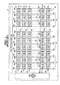
- Fig. 1 illustrates a configuration of a conventional active matrix OLED 10.
- the conventional active matrix OLED 10 includes a pixel portion 100, a gate line driving circuit 110, a data line driving circuit 120 and a control unit (not shown).
- the pixel portion 100 includes a plurality of gate lines 111 - 11 m to which scan signals S1 - Sm are provided from the gate line driving circuit 110, a plurality of data lines 121 (121R, 121G, 121B) - 12n (12nR, 12nG, 12nB) for supplying data signals (DR1, DG1, DB1) - (DRn, DGn, DBn) from the data line driving circuit 120, and a plurality of power lines 131 (131R, 131G, 131B) to 13n (13nR, 13nG, 13nB) for providing power supply voltages VDD1 - VDDn.
- a plurality of pixels P11 - Pmn connected to the plurality of gate lines 111 - 11 m, the plurality of data lines 121 - 12n, and the plurality of power lines 131 - 13n are arranged in a matrix form.
- Each of the pixels P11 - Pmn is composed of three unit pixels, i.e., R, G and B unit pixels (PR11, PG11, PB11) - (PRmn, PGmn, PBmn), and is connected to the corresponding one gate line, one data line and one power supply line of the plurality of gate lines, data lines, and power supply lines.
- the pixel P11 is composed of an R unit pixel PR11, a G unit pixel PG11 and a B unit pixel PB11.
- the pixel P11 is connected to a first gate line 111 of the plurality of gate lines 111 - 11 m that provides a first scan signal S1, a first data line of the plurality of data lines 121 - 12n, and a first power line 131 of the plurality of power lines 131 - 13n.
- the R unit pixel PR11 of the pixel P11 is connected to the first gate line 111, an R data line 121R, to which an R data signal DR1 is provided, of the first data lines 121, and an R power line 131 R of the first power lines 131.
- the G unit pixel PG11 is connected to the first gate line 111, a G data line 121G, to which a G data signal DG1 is provided, of the first data lines 121, and a G power line 131G of the first power lines 131.
- the B unit pixel PB11 is connected to the first gate line 111, a B data line 121B, to which a B data signal DB1 is provided, of the first data lines 121, and a B power line 131B of the first power lines 131.
- Fig. 2 shows a pixel circuit of the conventional OLED, illustrating a circuit diagram of one pixel P11 composed of R, G and B unit pixels.
- the R unit pixel PR11 of the R, G and B unit pixels PR11, PG11, PB11 constituting the pixel P11 includes a switching transistor M1_R in which the scan signal S1 applied from the first gate line 111 is provided to a gate, and the data signal DR1 from the R data line 121 R is provided to a source.
- the R unit pixel PR11 also includes a driving transistor M2_R in which a gate is connected to a drain of the switching transistor M1_R and the power supply voltage VDD1 from the power supply line 131 R is provided to a source.
- a capacitor C1_R is connected between the gate and the source of the driving transistor M2_R.
- the R unit pixel PR11 includes an R EL element EL1_R in which an anode is connected to a drain of the driving transistor M2_R and a cathode is connected to a ground voltage VSS.
- the G unit pixel PG11 includes: a switching transistor M1_G in which the scan signal S1 applied from the first gate line 111 is provided to a gate, and the data signal DG1 from the G data line 121 G is provided to a source.
- the G unit pixel PG11 also includes a driving transistor M2_G in which a gate is connected to a drain of the switching transistor M1_G and the power supply voltage VDD1 from the power supply line 131G is provided to a source.
- a capacitor C1_G is connected between the gate and the source of the driving transistor M2_G.
- the G unit pixel PG11 includes a G EL element EL1_G in which an anode is connected to a drain of the driving transistor M2_G and a cathode is connected to the ground Vss.
- the B unit pixel PB11 includes a switching transistor M1_B in which the scan signal S1 applied from the first gate line 111 is provided to a gate and the data signal DB1 from the B data line 121 B is provided to a source.
- the B unit pixel PB11 also includes a driving transistor M2_B in which a gate is connected to a drain of the switching transistor M1_B and the power supply voltage VDD1 from the power supply line 131B is provided to a source.
- a capacitor C1_B is connected between the gate and the source of the driving transistor M2_B.
- the B unit pixel PB11 includes a B EL element EL1_B in which an anode is connected to the drain of the driving transistor M2_B and a cathode is connected to the ground voltage VSS.
- the switching transistors M1_R, M1_G, M1_B of the R, G and B unit pixels constituting the pixel P11 are driven thereby, and the R, G and B data DR1, DG1, DB1 from the R, G and B data lines 121R, 121G, 121B are applied, respectively, to the gates of the driving transistors M2_R, M2_G, and M2_B.
- the driving transistors M2_R, M2_G, M2_G provide the EL elements EL1_R, EL1_G, EL1_B with respective driving currents corresponding to a difference between the data signals DR1, DG1, DB1 applied to the gates and the power supply voltage VDD1 supplied from respective R, G and B power supply lines 131R, 131G, 131B.
- the EL elements EL1_R, EL1_G. EL1_B are driven by the driving currents applied through the respective driving transistors M2_R, M2_G, M2_B, thereby resulting in driving the pixel P11.
- the capacitors C1_R, C1_G, C1_B store the respective data signals DR1, DG1, DB1 applied to the R, G and B data lines 121R, 121G and 121B.
- the first gate line is driven, and then, the pixels P11-P1n connected to the first gate line 111 are driven.
- the switching transistors of the R, G and B unit pixels (PR11 - PR1n), (PG11 - PG1n), (PB11 - PB1n) of the pixels P11- P1n connected to the first gate line 111 are driven by the scan signal S1 applied to the first gate line 111.
- the R, G and B data signals D(S1) (DR1 - DRn), (DG1 - DGn), (DB1 - DBn) from the R, G and B data lines (121R - 12nR), (121G - 12nG), (121 B - 12nB) constituting the first to the n th data lines 121 to 12n are respectively applied to the gates of the driving transistors of the R, G and B unit pixels at the same time.
- the driving transistors of the R, G and B unit pixels provide the R, G and B EL elements with the driving currents corresponding to the R, G and B data signals D (S1) (DR1 to DRn), (DG1 to DGn), (DB1 to DBn) each applied to the R, G and B data lines 121R to 121nR, 121G to 12nG, 121B to 12nB. Therefore, when the scan signal S1 is applied to the first gate line 111, the EL elements constituting the R, G and B unit pixels (PR11 - PR1n), (PG11 - PG1n), (PB11 - PB1n) of the pixels P11 - P1n connected to the first gate line 111 are driven at the same time.
- data signals D(S2) (DR1 - DRn), (DG1 - DGn), (DB1 - DBn) from the R, G and B data lines (121R - 12nR), (121 G - 12nG), (121 B - 12nB) constituting the first to the n th data lines 121 to 12n are applied to the R, G and B unit pixels (PR21 - PR2n), (PG21 - PG2n), (PB21 - PB2n) of the pixels (P21 - P2n) connected to the second gate line 112.
- the EL elements constituting the R, G and B unit pixels (PR21 - PR2n), (PG21 - PG2n), (PB21 - PB2n) of the pixels (P21 - P2n) connected to the second gate line 112 are simultaneously driven by the driving currents corresponding to the data signals D (S2)(DR1- DRn), (DG1- DGn), (DB1 -DBn).
- the EL elements constituting the R, G and B unit pixels PRm1 - PRmn), (PGm1 - PGmn), (PBm1 - PBmn) of the pixels (Pm1 - Pmn) connected to the m th gate line 11 m are simultaneously driven according to the R, G and B data signals D(Sm) (DR1 - DRn), (DG1 - DGn), (DB1 - DBn) applied to the R, G and B data lines (121R - 12nR), (121G - 12nG), (121B - 12nB).
- the scan signals S1 - Sm are sequentially applied from the first gate line 111 to the m th gate line 11 m, the pixels (P11 - P1 n) - (Pm1 - Pmn) connected to each gate line 111 - 11 m are sequentially driven, thereby displaying a picture by driving the pixels during one frame 1 F.
- each pixel is composed of three R, G and B unit pixels, and by each R, G and B unit pixel, the driving devices, that is, a switching thin film transistor and a driving thin film transistor and a capacitor, for driving the R, G and B EL elements, are arranged. Further, the data line and a power supply line for providing the data signal and the power supply (ELVDD) to each driving device are respectively arranged in each unit pixel.
- the driving devices that is, a switching thin film transistor and a driving thin film transistor and a capacitor, for driving the R, G and B EL elements.
- the conventional display device has problems in that, as a plurality of lines and a plurality of devices are arranged in each pixel, a circuit constitution is complex, and thus, a probability that a defect is generated is increased, thereby lowering yield.
- each pixel area is reduced, and thus, it is difficult to arrange many devices in one pixel, and the aperture ratio is also reduced.
- the present invention relates to an organic light emitting display as defined by claims 1-4.
- an OLED display 50 includes a pixel portion 500, a gate line driving circuit 510, a data line driving circuit 520, and a light emitting control signal generation circuit 590.
- the gate line driving circuit 510 sequentially generates scan signals S1 - Sm to the gate lines of the pixel portion 500 during one frame.
- the data line driving circuit 520 sequentially provides R, G and B data signals (D1a - D1c) ⁇ (Dna - Dnc) to the data lines of the pixel portion 500 each time the scan signal is applied during one frame.
- the light emitting control signal generation circuit 590 sequentially generates the light emitting control signals (EC_11, 21) - (EC_1m, 2m), for controlling the light emitting of the R, G and B EL elements, to the light emitting control lines each time the scan signal is applied during one frame.
- the pixel portion 500 includes a plurality of gate lines 511 - 51 m to which respective scan signals S1 - Sm from the gate line driving circuit 510 are provided, and a plurality of data lines (521 a - 521 c) ⁇ (52na - 52nc) to which respective data signals (D1a - D1c) ⁇ (Dna - Dnc) from the data line driving circuit 520 are applied.
- the pixel portion 500 also includes a plurality of light emitting control lines (591a, 591b) ⁇ (59ma, 59mb) to which respective light emitting control signals (EC_11, EC_21) ⁇ (EC_1 m, 2m) from the light emitting control signal generation circuit 590 are provided, and a plurality of power supply lines (531a - 531c) ⁇ (53na - 53nc) to which respective power supply voltages (VDD1a - VDD1c) ⁇ (VDDna - VDDnc) are provided.
- the pixel portion 500 also includes a plurality of pixels connected to the plurality of gate lines (511 - 51m), the plurality of data lines (521 a - 521c) ⁇ (52na - 52nc), the plurality of light emitting control lines (591 a, 591b - 59ma, 59mb), and the plurality of power supply lines (531a - 531c) ⁇ (53na - 53nc), and arranged in a matrix form.
- Two adjacent pixels (P11, P12) ⁇ (Pm2n-1, Pm2n) along the gate line among the plurality of pixels P11 - Pm2n are connected to a corresponding one of the plurality of gate lines 511 - 51 m, three corresponding data lines among the plurality of data lines (521a - 521c) ⁇ (52na - 52nc), two corresponding light emitting control lines among the plurality of light emitting control lines (591a - 591b) ⁇ (59ma - 59mb), and three corresponding power supply lines among the plurality of power supply lines (531a - 531c) ⁇ (53na - 53nc).
- two adjacent pixels P11, P12 are connected to the gate line 511 that provides the first scan signal S1 among the plurality of gate lines 511 - 51m, the data lines 521 a - 521c that provide the data signals D1 a - D1c among the plurality of data lines (521a - 521c) ⁇ (52na - 52nc), the light emitting control lines 591a, 591b that generate light emitting control signals EC_11, EC_21 among the plurality of light emitting control lines (591 a, 591 b) - (59ma, 59mb), and the power supply lines 531a - 531c among the plurality of power supply lines (531a - 531c) ⁇ (53na - 53nc).
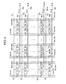
- Fig. 8 is a block configuration diagram schematically illustrating a pixel circuit of two adjacent pixels, for the OLED display according to the first exemplary embodiment of the present invention shown in Fig. 6.
- Fig. 8 shows two adjacent pixels P11, P12 among the plurality of pixels for illustrative purposes only with the understanding that the other pairs of adjacent pixels shown in FIG. 6 have substantially the same configuration and operate in substantially the same manner.
- two adjacent pixels P11, P12 includes a display element 560 having R, G and B EL elements (EL1_R, EL1_G, EL1_B) 532a, (EL2_R, EL2_G, EL2_B) 532b, and first to third active devices ("active elements") 570a - 570c for driving the R, G and B EL elements (EL1_R, EL1_G, EL1_B), (EL2_R, EL2_G, EL2_B).
- the first active device 570a is connected to the gate line 511, the data line 521a, the light emitting control lines 591 a, 591 b and the power supply line 531 a.
- the second active device 570b is connected to the gate line 511, the data line 521b, the light emitting control lines 591a, 591 b, and the power supply line 531 b.
- the third active device 570c is connected to the gate line 511, the data line 521 c, the light emitting control lines 59 1 a, 591 b and the power supply line 531c.
- anode and cathode electrodes of R and G EL elements EL1_R, EL1_G among the R, G and B EL elements EL1_R, EL1_G, EL1_B of the first pixel P11 are connected between the first active device 570a and the ground VSS.
- anode and cathode electrodes of a B EL element EL1_B of the first pixel P11 and an R EL element EL2_R among the R, G and B EL elements EL2_R, EL2_G, EL2_B of the second pixel P12 are connected.
- the anode and cathode electrodes of the G and B EL elements EL2_G, EL2_B of the second pixel P12 are connected between the third active device 570c and the ground.
- two EL elements (EL1_R, EL1_G), (EL1_B. EL2_R) or (EL2_G, EL2_B) among R, G and B EL elements (EL1_R, EL1_G, EL1_B) 532a, (EL2_R, EL2_G, EL2_B) 532b of two adjacent pixels P11, P12 share a corresponding one of the active devices 570a, 570b and 570c. Therefore, two EL elements (EL1_R, EL1_G). (EL1_B. EL2_R) or (EL2_G, EL2_B) that share the corresponding one of the active devices 570a, 570b and 570c are time-divisionally sequentially driven by subframes constituting one frame.
- the R, G and B EL elements (EL1_R, EL1_G, EL1_B) 532a, (EL2_R, EL2_G, EL2_B) 532b of two pixels P11, P12, the EL elements EL1_R, EL1_B, EL2_G among R, G and B EL elements (EL1_R, EL1_G, EL1_B), (EL2_R, EL2_G, EL2_B) sharing one active device 570a, 570b or 570c are grouped into a first EL element group, and the remaining EL elements EL1_G, EL2_R, EL2_B are grouped into a second EL element group.
- the EL elements EL1_R, EL1_B, EL2_G belonging to the first EL element group of two EL element groups are substantially simultaneously driven, and then the EL elements EL1_G, EL2_R, EL2_B belonging to the second EL element group are substantially simultaneously driven in the next subframe.
- one frame is divided into two subframes, and two light emitting elements (EL1_R, EL1_G), (EL1_B, EL2_R), (EL2_G, EL2_B) among R, G and B EL elements (EL1_R, EL1_G, EL1_B), (EL2_R, EL2_G, EL2_B) of two adjacent pixels are respectively driven time-divisionally by each active device (570a, 570b, 570c) by subframes.
- the light emitting elements EL1_R, EL1_B and EL2_G are substantially simultaneously driven in one subframe by the respective active devices 570a, 570b, 570c and in the next frame, the light emitting elements EL1_G, EL2_R and EL2_B are substantially simultaneously driven by respective active devices 570a, 570b, 570c, thereby driving the adjacent pixels P11, P12 and displaying a predetermined color.
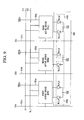
- Fig. 10 illustrates a block configuration diagram of a pixel circuit in the OLED display with a sequential driving method according to the first exemplary embodiment of the present invention of Fig. 8, and Fig. 12 illustrates a pixel circuit that can be applied as the pixel circuit of Fig. 10.
- the pixel circuits of Fig. 10 and Fig. 12 illustrate a detailed example of the pixel circuit for sequentially driving the R, G and B EL elements EL1_R, EL1_G, EL1_B, EL2_R, EL2_G, EL2_B of two adjacent pixels P11, P12 by time division during one frame.
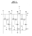
- the first active device 570a for driving a first display device 560a includes a first drive device 571 a and a first sequential control device 575a.
- the first drive device 571 a includes a first P-type thin film transistor M51a having a gate connected to the gate line 511 and a source connected to the data line 521 a; a second P-type thin film transistor M52a having a source connected to the power supply line 531 a and a gate connected to a drain of the first thin film transistor; and a capacitor C51 a connected between the power supply line 531 a and the gate of the second thin film transistor M52a.
- the first sequential control device 575a includes a third P-type thin film transistor M53a having the light emitting control signal EC_11 from the light emitting control line 591 a applied to a gate, and a source connected to a drain of the second thin film transistor M52a; and a fourth P-type thin film transistor M54a having the light emitting control signal EC_21 from the light emitting control line 591 b applied to a gate, and a source connected to the drain of the second thin film transistor M52a.
- the first display device 560a includes an R EL element EL1_R of the first pixel P11 having an anode electrode and a cathode electrode respectively connected to a drain of the third thin film transistor M53a and the ground; and a G EL element EL1_G of the first pixel P11 having an anode electrode and a cathode electrode respectively connected to a drain of the fourth thin film transistor M54a and the ground.
- the second active device 570b for driving a second display device 560b includes a second drive device 571 b and a second sequential control device 575b.
- the second drive device 571 b includes a first P-type thin film transistor M51 b having a gate connected to the gate line 511 and a source connected to the data line 521b; and a second P-type thin film transistor M52b having a source connected to the power supply line 531 b and a gate connected to a drain of the first thin film transistor M51b; and a capacitor connected between the power supply line 531b and the gate of the second thin film transistor M52b.
- the second sequential control device 575b includes a third P-type thin film transistor M53b having the light emitting control signal EC_11 from the light emitting control line 591a applied to a gate, and a source connected to a drain of the second thin film transistor M52b; and a fourth P-type thin film transistor M54b having the light emitting control signal EC_21 from the light emitting control line 591 b applied to a gate, and a source connected to the drain of the second thin film transistor M52b.
- the second display device 560b includes a B EL element EL1_B of the first pixel P11 having an anode electrode and a cathode electrode respectively connected to a drain of the third thin film transistor M53b and the ground; and an R EL element EL2_R of the second pixel P12 having an anode and a cathode respectively connected to a drain of the fourth thin film transistor M54b and the ground.
- the third active device 570c for driving a third display device 560c includes a third drive device 571 c and a third sequential control device 575c.
- the third drive device 571 c includes a first P-type thin film transistor M51 c having a gate connected to the gate line 511 and a source connected to the data line 521c; and a second P-type thin film transistor M52c having a source connected to the power supply line 531 c and a gate connected to a drain of the first thin film transistor M51 c; and a capacitor C51 c connected between the power supply line 531c and the gate of the second thin film transistor M52c.
- the third sequential control device 575c includes a third P-type thin film transistor M53c having the light emitting control signal EC_11 from the light emitting control line 591 a applied to a gate, and a source connected to a drain of the second thin film transistor M52c; and a fourth P-type thin film transistor M54c having the light emitting control signal EC_21 from the light emitting control line 591 b applied to a gate, and a source connected to the drain of the second thin film transistor M52c.
- the third display device 560c includes a G EL element EL2_G of the second pixel P12 having an anode electrode and a cathode electrode respectively connected to a drain of the third thin film transistor M53c and the ground; and a B EL element EL2_B of the second pixel P12 having an anode and a cathode respectively connected to a drain of the fourth thin film transistor M54c and the ground.
- each one of scan signals S1 - Sm from the gate line driving circuit 110 is sequentially applied to a plurality of gate lines, so that m scan signals are applied thereto during one frame.
- R, G and B data signals (DR1 - DRn), (DG1 - DGn), (DB1 - DBn) from the data line driving circuit 120 are simultaneously applied to R, G and B data lines to drive the pixels.
- one frame is divided into two subframes, and during each subframe, the scan signal from the gate line driving circuit 510 is applied to each gate line, and thus, 2m scan signals are applied during one frame.
- the switching transistors M51a - M51 c of the first to third drive devices 571a - 571 c are turned on, and the R data signal D1a and the B data signal D1b of the first pixel P11 and the G data signal D1c of the second pixel P12 are provided to the driving transistors M52a - M52c from the data lines 521a - 521c.
- the R EL element EL1_R and B EL element EL1_B of the first pixel and the G EL element EL2_G of the second pixel are substantially simultaneously driven corresponding to the R data signal D1a and the B data signal D1b of the first pixel P11 and the G data signal D1c of the second pixel P12.
- the scan signal S1 is applied to the first gate line 511, so that the G data signal D1a of the fist pixel P11 and the R data signal D1b and the B data signal D1c of the second pixel P12 are provided from the data lines 521 a - 521 c to the driving transistors M52a - M52c.
- the thin film transistors M54a - M54c are turned on by the light emitting control signal EC_21 provided from the light emitting control line 591 b, so that the G EL element EL1_G of the first pixel P11 and the R EL element EL2_R and the B EL element EL2_B of the second pixel P12 are substantially simultaneously driven corresponding to the G data signal D1 a of the first pixel P11 and the R data signal D1b and the B data signal D1c of the second pixel P12.
- the R, G and B EL elements of the two pixels can be time-divisionally driven during one frame. That is, referring to Fig.
- EL1_R, EL1_B, EL2_G among the R, G and B EL elements (EL1_R, EL1_G, EL1_B), (EL2_R, EL2_G, EL2_B) of the first and second pixels (P11, P12) into the first group, and EL1_G, EL2_R, EL2_B into the second group, the first group of EL elements (EL1_R, EL1_B, EL2_G) during the first subframe, and the second group of EL elements (EL1_G. EL2_R, EL2_B) during the second subframe are driven to display the picture.
- the EL elements having different colors simultaneously emit light during one subframe, two or more different colors emit light within one subframe.
- the active devices 570a - 570c are shared by grouping the R, G and B EL elements of two adjacent pixels by two, thereby simplifying the circuit configuration.
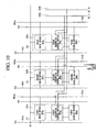
- Fig. 13 has almost the same configuration as the detailed circuit of the pixel portion shown in Fig. 12. It can be seen in FIG. 13 that a second sequential control device 575b' is configured slightly differently from that of the second sequential control device 575b of Figs. 11 and 12, while the rest of the pixel circuit elements are substantially the same.
- the second sequential control device 575b' has a third P-type thin film transistor M53b' having the light emitting control signal EC_21 from the light emitting control line 591 b applied to a gate, and a source connected to a drain of the second thin film transistor M52b; and a fourth P-type thin film transistor M54b' having the light emitting control signal EC_11 from the light emitting control line 591 a applied to a gate, and a source connected to the drain of the second thin film transistor M52b.
- the R EL element EL1_R of the first pixel P11 and the R and G EL elements EL2_R, EL2_G of the second pixel P12 are grouped into the first group of EL elements
- the G and B EL elements EL1_G, EL1_B of the first pixel P11 and the B EL element EL2_B of the second pixel P12 are grouped into the second group of EL elements. Therefore, in the first subframe of one frame, the first group of EL elements, the R EL element EL1_R of the first pixel P11 and the R and G EL element EL2_R, EL2_G of the second pixel P12, are substantially simultaneously driven.
- the second group of EL elements the G and the B EL element EL1_G, EL1_B of the first pixel P11 and the B EL element EL2_B of the second pixel P12, are substantially simultaneously driven.
- FIGs. 12 and 13 only illustrate grouping of the R, G and B EL elements of the first and second pixels P11, P12 arranged on the same first gate line, for those adjacent pixels as shown in Fig. 6, the EL elements of two adjacent pixels are grouped into the first and second groups in substantially the same manner as described above.
- Fig. 15 is an operational waveform diagram for illustrating a method of sequentially driving the OLED display of Fig. 4 by time division, which shows an operational waveform diagram of the sequential light emitting method that sequentially light emit the EL elements by scan line within each subframe.
- a method of driving the OLED in the sequential light emitting method will be described as follows with reference to the operational waveform diagram of Fig. 15.
- the first gate line 511 is driven. Further, the data signals for driving the EL elements belonging to the first group among the R, G and B EL elements of the pixels P11 - P12n connected to the first gate line 511 are provided to the corresponding driving transistors as the data signals (D1a - D1c) ⁇ (Dna - Dnc) from the data line driving circuit 520 .
- the thin film transistors for controlling the EL elements belonging to the first group among the thin film transistors constituting the sequential control devices are turned on, so that the driving currents corresponding to the data signals (D1a - D1c) ⁇ (Dna - Dnc) are provided to drive the EL elements of the first group.
- the data signals (D1a - D1c) ⁇ (Dna - Dnc) for driving the EL elements belonging to the second group are provided through the data lines (521a - 521c) - (52na - 52nc) to the corresponding transistors.
- the thin film transistors for controlling the second group of EL elements among the thin film transistors of the sequential control devices are turned on, so that the driving currents corresponding to the data signals (D1a - D1c) - (Dna - Dnc) are provided to drive the EL elements of the second group.
- the data signals (D1a - D1c) ⁇ (Dna - Dnc) are sequentially applied to the data lines (521 a - 521c) ⁇ (52na - 52nc).
- the light emitting control signals (EC_11, EC_21) ⁇ (EC_1m, EC_2m) for sequentially controlling the R, G and B EL elements of two adjacent pixels among pixels (P11 - P12n) - (Pm1 - Pm2n) connected to the gate lines 511 - 51 m from the light emitting control signal generation circuit 590 through light emitting control lines 591 a, 591 b are sequentially generated to the sequential control devices.
- the thin film transistors corresponding to the first EL element group among the thin film transistors of the sequential control devices are turned on to drive the EL elements of the first group according to the data signals (D1a - D1c) ⁇ (Dna - Dnc).
- the thin film transistors corresponding to the second EL element group among the thin film transistors of the sequential control devices are turned on to drive the EL elements of the second group according to the data signals (D1a - D1c) ⁇ (Dna - Dnc).
- one frame is divided into two subframes, and in the first subframe, the EL elements grouped into the first group among the R, G and B EL elements of two adjacent pixels among pixels connected to the first to m th gate lines 511 - 51 m are sequentially driven. Further, in the second subframe, the EL elements grouped into the second group are sequentially driven, thereby sequentially driving the EL elements grouped into the first group and the EL elements grouped into the second group and displaying the picture, by each subframe within one frame.
- Fig. 17 is another operational waveform diagram for illustrating a method of sequentially driving the OLED display of Fig. 4 by time division, which is a collective light emitting method that collectively light emit the EL elements connected to the scan line in each subframe.
- a method of driving the OLED display by a collective light emitting method will now be described as follows with reference to the operational waveform diagram of Fig. 17.
- the collective light emitting method divides one frame 1 F into two subframes 1SF, 2SF, and divides again each subframe 1SF, 2SF into a data write period and a pixel light emitting period.
- the data write period of the first subframe 1SF when the scan signals S1 - Sm are sequentially applied from the gate line driving circuit 510 to the fist gate line 511 to the m th gate line 51m, the data signals (D1a - D1c) ⁇ (Dna - Dnc) for driving the EL elements belonging to the first group among the R, G and B EL elements of the pixels (P11 - P12n) ⁇ (Pm1 - Pm2n) connected to the first gate line 511 to the m th gate line 51m are sequentially provided to each corresponding driving transistor from the data line driving circuit 520.
- low-state light emitting control signals EC_11 - EC1m and high-state light emitting control signals EC_21 - EC_2m are respectively provided at the same time to each of the light emitting control lines (591a - 59ma) and (591 b - 59mb) from the light emitting control signal generation circuit 590, so that the thin film transistors for controlling the EL elements belonging to the first group among the thin film transistors of the sequential control devices are substantially simultaneously turned on.
- the driving currents corresponding to the data signals (D1a - D1c) ⁇ (Dna - Dnc) are substantially simultaneously provided to the EL elements of the first group, thereby collectively light emitting the EL elements of the first group.
- data signals (D1a - D1c) ⁇ (Dna - Dnc) for driving the EL elements belonging to the second group among the R, G and B EL elements of pixels (P11 - P12n) ⁇ (Pm1 - Pm2n) connected to the first gate line 511 to the m th gate line 51 m are sequentially provided to each corresponding driving transistor from the data line driving circuit 520.
- high-state light emitting control signals EC_11 - EC1 m and low-state light emitting control signals EC_21 - EC_2m are substantially simultaneously provided to each of the light emitting control lines (591a - 59ma) and (591b - 59mb) from the light emitting control signal generation circuit 590 respectively, so that the thin film transistors for controlling the EL elements belonging to the second group among the thin film transistors of the sequential control devices are substantially simultaneously turned on.
- the driving currents corresponding to the data signals (D1a - D1c) ⁇ (Dna - Dnc) are substantially simultaneously provided to the EL elements of the second group, thereby collectively light emitting the EL elements of the second group. In this manner, the picture is displayed within one frame.
- an OLED display 50' is almost identical to the OLED display 50 of Figs. 4 and 6.
- the light emitting control signals (EC_11, EC_21) ⁇ (EC_1m, EC_2m) are provided from the light emitting control signal generation circuit 590 through each pair of light emitting control lines (591a, 591 b) - (59ma, 59mb) to the pixels (P11 - P12n) ⁇ (Pm1 - Pm2n) arranged in the same scan line.
- the light emitting control signals EC_1 ⁇ EC_m are provided from a light emitting control signal generation circuit 590' through one light emitting control line 591 - 59m to pixels (P11' - P12n') ⁇ (Pm1' - Pm2n') arranged in the same scan line.
- Fig. 9 is a block configuration diagram that schematically illustrates the pixel circuit of two adjacent pixels, in the OLED display 50' according to the second exemplary embodiment of the present invention shown in Fig. 7, and Fig. 11 illustrates a detailed block configuration diagram of the pixel circuit of Fig. 9.
- Fig. 14 illustrates an example of the detailed configuration of the pixel circuit shown in Figs. 9 and 11.
- Figs. 9, 11 and 14 only two adjacent pixels, i.e., the first and second pixels P11', P12' are shown for illustrative purposes.
- two adjacent pixels P11', P12' include a display element 560 having the R, G and B EL elements (EL1_R, EL1_G, EL1_B) 532a, (EL2_R, EL2_G, EL2_B) 532b, and first to third active elements ("active devices") 570a' - 570c' for driving the R, G and B EL elements (EL1_R, EL1_G, EL1_B) 532a, (EL2_R, EL2_G, EL2_B) 532b.
- the first to third active elements 570a' - 570c' respectively include the first to third drive devices 571 a - 571c and the sequential control devices 575a" - 575c".
- the first to third drive devices 571a - 571c of the first to third active elements 570a' - 570c' have the same configuration as the corresponding elements of the first exemplary embodiment as illustrated in Fig. 12.
- the grouping method of the display element 560 having the first to third display devices 560a - 560c is also the same as that of the pixel circuit of the first exemplary embodiment as illustrated in Fig. 12.
- the first sequential control device 575a" of the first active element 570a' includes a P-type thin film transistor M53a" having a light emitting control signal EC_1 provided through the light emitting control line 591 applied to a gate, a source connected to a drain of the driving transistor M52a of the drive device 571 a, and a drain connected to an anode electrode of the EL element EL1_R of the display device 560a.
- the first sequential control device 575a" also includes an N-type thin film transistor M54a" having the light emitting control signal EC_1 applied to a gate through the light emitting control line 591, a drain connected to the driving transistor M52a of the drive device 571 a, and a source connected to the anode electrode of the EL element EL1_G of the display device 560a.
- the second sequential control device 575b" of the second active element 570b' includes a P-type thin film transistor M53b" having the light emitting control signal EC_1 applied to a gate through the light emitting control line 591, a source connected to a drain of the driving transistor M52b of the drive device 571 b, and a drain connected to the anode electrode of the EL element EL1_B of the display device 560b.
- the second sequential control device 575b" also includes an N-type thin film transistor M54b" having the light emitting control signal EC_1 applied to a gate through the light emitting control line 591, a drain connected to the drain of the driving transistor M52b of the drive device 571 b, and a source connected to the anode electrode of the EL element EL2_R of the display device 560b.
- the third sequential control device 575c" of the third active element 570c' includes a P-type thin film transistor M53c" having the light emitting control signal EC_1 provided through the light emitting control line 591 applied to a gate, a source connected to the drain of the driving transistor M52c of the drive device, and a drain connected to the anode electrode of the EL element EL2_G of the display device 560c.
- the third sequential control device 575c" also includes an N-type thin film transistor M54c" having the light emitting control signal EC_1 provided through the light emitting control line 591 applied to a gate, a drain connected to the drain of the driving transistor M52c of the drive device 571c, and a source connected to the anode electrode of the EL element EL2_B of the display device 560c.
- each of the sequential control devices 575a - 575c includes a P-type thin film transistor and an N-type thin film transistor, and is identical to the method of driving the pixel circuit of the first exemplary embodiment except that the second exemplary embodiment is controlled through only one light emitting control signal per scan line.
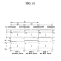
- Fig. 16 is an operational waveform diagram for illustrating a method of time-divisionally driving the OLED display of Fig. 5, which is a sequential light emitting method that sequentially light emit the EL elements by scan line within each subframe.
- a method of driving the OLED display by sequential light emitting method will now be described as follows with reference to the operational waveform diagram of Fig. 16.
- the scan signal S1 is applied form the gate line driving circuit 510 to the first gate line 511
- the first gate line 511 is driven, and the data signals, as (D1a - D1c) ⁇ (Dna - Dnc), for driving the EL elements belonging to the first group among the R, G and B EL elements of the pixels P11' - P2n' connected to the first gate line 511 from the data line driving circuit 520 are provided to the corresponding driving transistors.
- the low-state light emitting control signal EC_1 through the light emitting control line 591 from the light emitting control signal generation circuit 590' is generated, only the p-type thin film transistors for controlling the EL elements belonging to the first group among the thin film transistors constituting the sequential control device are turned on, so that the driving currents corresponding to the data signals (D1a - D1c) ⁇ (Dna - Dnc) are provided to drive the EL elements of the first group.
- the data signals (D1a - D1c) ⁇ (Dna - Dnc) for driving the EL elements belonging to the second group are provided to the data lines (521a - 521c) ⁇ (52na - 52nc), so that the driving transistors corresponding to the EL elements belonging to the second group are driven.
- n-type thin film transistors for controlling the EL elements belonging to the second group among the thin film transistors of the sequential control devices are turned on, and the driving currents corresponding to the data signals (D1a - D1c) ⁇ (Dna - Dnc) are provided to drive the EL elements of the second group.
- the scan signals are applied to the gate lines 511 - 51 m by each subframe of one frame by repeating the operation as illustrated above, the data signals (521a - 521c) ⁇ (52na - 52nc) are sequentially applied to the data lines (521a - 521c) ⁇ (52na - 52nc), and the light emitting control signals EC_1 - EC_m for sequentially controlling the R, G and B EL elements of two adjacent pixels among pixels (P11' - P12n') ⁇ (Pm1' - Pm2n') connected to the gate line (511 - 51 m) through the light emitting control line 591 from the light emitting control signal generation circuit 590' are sequentially applied to the sequential control devices.
- the p-type thin film transistors corresponding to the first group of EL elements among the thin film transistors of the sequential control devices are turned on, and based on the data signals (D1a - D1c) ⁇ (Dna - Dnc), the EL elements of the first group are driven.
- the n-type thin film transistors corresponding to the second group of EL elements among the thin film transistors of the sequential control devices are turned on, so that based on the data signals (D1a - D1c) ⁇ (Dna - Dnc), the EL elements of the second group are driven.
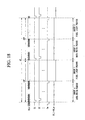
- Fig. 18 is another operational waveform diagram for illustrating a method of time-divisionally driving the OLED display of Fig. 5, which is a collective light emitting method that collectively light emit the EL elements connected to the scan line within each subframe.
- a method of driving the OLED display by the collective light emitting method will now be described as follows with reference to the operational waveform of Fig. 18.
- the data signals (D1a - D1c) ⁇ (Dna - Dnc) for driving the EL elements belonging to the first group among the R, G and B EL elements of the pixels (P11' - P12n') ⁇ (Pm1' - Pm2n') connected to the first gate line 511 to the m th gate line 51 m are provided to the corresponding driving transistors from the data line driving circuit 520.
- low-state light emitting control signals EC_1 - EC_m from the light emitting control signal generation circuit 590' are substantially simultaneously provided to the light emitting control lines 591 - 59m, so that the thin film transistors for controlling the EL elements belonging to the first group among the thin film transistors of the sequential control devices are substantially simultaneously turned on. Therefore, the driving currents corresponding to the data signals (D1a - D1c) ⁇ (Dna - Dnc) are substantially simultaneously provided to the EL elements of the first group, so that the EL elements of the first group collectively emit light at substantially the same time.
- high-state light emitting control signals EC_1 - EC_m are substantially simultaneously provided from the light emitting control signal generation circuit 590' to each of the light emitting control lines 591 - 59m, so that thin film transistors for controlling the EL elements belonging to the second group among the thin film transistors of the sequential control devices are substantially simultaneously turned on. Therefore, the driving currents corresponding to the data signals (D1a - D1c) ⁇ (Dna - Dnc) are substantially simultaneously provided to the second group of EL elements, so that the EL elements of the second group collectively emit light at substantially the same time. In this manner, the picture is displayed in one frame.
- the method of driving the OLED display according to the first and second exemplary embodiments of the present invention divides one frame into two subframes, and in the first subframe, sequentially or collectively drives the EL elements grouped into the first group among the R, G and B EL elements of two adjacent pixels among the pixels connected to the first to the m th gate line (511 - 51m). Further, in the second subframe, the method sequentially or collectively drives the EL elements grouped into the second group. This way, the EL elements grouped into the first group and the EL elements grouped into the second group are time-divisionally driven, and the picture is displayed by each subframe within one frame.
- R, G and B EL elements of two adjacent pixels are classified into two groups and are time-divisionally driven by each subframe where grouping the EL elements belonging to the first group and the EL elements belonging to the second group are arbitrarily changeable, and the driving sequence of the first and second EL groups is also changeable.
- one or more pixels of the OLED display may also include white (W) EL elements instead of or in addition to one of more of R, G and B EL elements.
- the El elements may be arranged in a stripe type or a delta type.
- white balance can be adjusted by adjusting the light emitting time of the R, G and B EL elements.
- a turn-on time of the thin film transistor of the sequential control device that is, the duty ratio of the light emitting control signal, can be adjusted to adjust the light emitting time of the R, G and B EL elements, thereby adjusting the white balance.
- each of the first to third drive devices includes two thin film transistors, that is, the switching transistor and the driving transistor, and one capacitor.
- any configuration capable of driving the light emitting elements constituting the display device 560 may be used for the drive devices, and all methods capable of enhancing the driving characteristics of the light emitting element of the display device 560 may be used.
- a threshold voltage compensation device and/or other suitable devices may be added.
- the thin film transistors used in the first to third drive devices 571a - 571 c are P-type thin film transistors
- one or more N-type thin film transistors and/or a combination of N-type thin film transistors and P-type thin film transistors may be used instead.
- the N-type or P-type thin film transistor may be configured to operate in a depletion mode or in an enhancement mode.
- a various types of switching devices such as a thin film diode (TFD), a diode, and/or TRS (triodic rectifier switch), etc., may also be used.
- first to third sequential control devices 575a, 575b, 575c or 575a", 575b", 575c" are configured only with P-type thin film transistors or a combination of the N-type and P-type thin film transistors in the described exemplary embodiments
- the sequential control devices may also be configured with any other suitable combination of different types of transistors.
- the N-type thin film transistors or the P-type thin film transistors may be configured to operate in the depletion mode or in the enhancement mode.
- various different types of switching devices such as a TFD, a diode, a TRS (triodic rectifier switch), etc. may also be used.
- any suitable configuration may be used for the sequential control devices to sequentially drive the R, G and B EL elements.
- R, G and B EL elements driven with one active element are described as an example, the method of driving the R, G and B EL elements with one active element as illustrated in the exemplary embodiments of the present invention may also be applied to other light emitting element based display devices, such as a field emission display (FED), and the like.
- the light emitting elements may be Field Emission Diodes.
- the OLED display according to the exemplary embodiments of the present invention as illustrated above shares two EL elements driving thin film transistors and the switching thin film transistors among two adjacent R, G and B EL elements, thus driven by time division, thereby enabling high definition, reducing the number of the devices and lines, and enhancing the aperture ratio and yield.
Abstract
Description
- The present invention relates to an emissive display device and, more particularly, to an organic light emitting device (OLED) display and a method of time-divisionally driving two light emitting elements among R, G and B electroluminescent (EL) elements of two adjacent pixels.
-
US 6,421,033 B1 discloses an addressing scheme for use with current-driven emissive display devices having a single driving circuit connected to a plurality of adjacent light-emitting elements. An electrode of each of the plurality of adjacent light-emitting elements is connected to the single driving circuit and the other floats when the light-emitting element is switched off. - Recently, liquid crystal displays (LCDs) and OLED displays are widely used as portable information displays having features such as light weight, thin profile, and the like. The OLED displays have better performance in terms of luminance and wide viewing angle than LCDs, such that they attract an attention as next generation flat panel displays.
- Generally, in an active matrix OLED display, one pixel is composed of R, G and B unit pixels each including an EL element. In each EL element, an R, G or B organic emission layer is interposed between an anode electrode and G or B organic emission layer is interposed between an anode electrode and a cathode electrode, so that light is emitted from the R, G and B organic emission layers by voltages applied to the anode electrode and the cathode electrode.
- Fig. 1 illustrates a configuration of a conventional
active matrix OLED 10. - Referring to Fig. 1, the conventional active matrix OLED 10 includes a
pixel portion 100, a gateline driving circuit 110, a dataline driving circuit 120 and a control unit (not shown). Thepixel portion 100 includes a plurality of gate lines 111 - 11 m to which scan signals S1 - Sm are provided from the gateline driving circuit 110, a plurality of data lines 121 (121R, 121G, 121B) - 12n (12nR, 12nG, 12nB) for supplying data signals (DR1, DG1, DB1) - (DRn, DGn, DBn) from the dataline driving circuit 120, and a plurality of power lines 131 (131R, 131G, 131B) to 13n (13nR, 13nG, 13nB) for providing power supply voltages VDD1 - VDDn. - In the
pixel portion 100, a plurality of pixels P11 - Pmn connected to the plurality of gate lines 111 - 11 m, the plurality of data lines 121 - 12n, and the plurality of power lines 131 - 13n are arranged in a matrix form. Each of the pixels P11 - Pmn is composed of three unit pixels, i.e., R, G and B unit pixels (PR11, PG11, PB11) - (PRmn, PGmn, PBmn), and is connected to the corresponding one gate line, one data line and one power supply line of the plurality of gate lines, data lines, and power supply lines. - For example, the pixel P11 is composed of an R unit pixel PR11, a G unit pixel PG11 and a B unit pixel PB11. The pixel P11 is connected to a
first gate line 111 of the plurality of gate lines 111 - 11 m that provides a first scan signal S1, a first data line of the plurality of data lines 121 - 12n, and afirst power line 131 of the plurality of power lines 131 - 13n. - In other words, the R unit pixel PR11 of the pixel P11 is connected to the
first gate line 111, anR data line 121R, to which an R data signal DR1 is provided, of thefirst data lines 121, and anR power line 131 R of thefirst power lines 131. The G unit pixel PG11 is connected to thefirst gate line 111, aG data line 121G, to which a G data signal DG1 is provided, of thefirst data lines 121, and aG power line 131G of thefirst power lines 131. The B unit pixel PB11 is connected to thefirst gate line 111, aB data line 121B, to which a B data signal DB1 is provided, of thefirst data lines 121, and aB power line 131B of thefirst power lines 131. - Fig. 2 shows a pixel circuit of the conventional OLED, illustrating a circuit diagram of one pixel P11 composed of R, G and B unit pixels.
- Referring to Fig. 2, the R unit pixel PR11 of the R, G and B unit pixels PR11, PG11, PB11 constituting the pixel P11 includes a switching transistor M1_R in which the scan signal S1 applied from the
first gate line 111 is provided to a gate, and the data signal DR1 from theR data line 121 R is provided to a source. The R unit pixel PR11 also includes a driving transistor M2_R in which a gate is connected to a drain of the switching transistor M1_R and the power supply voltage VDD1 from thepower supply line 131 R is provided to a source. A capacitor C1_R is connected between the gate and the source of the driving transistor M2_R. In addition, the R unit pixel PR11 includes an R EL element EL1_R in which an anode is connected to a drain of the driving transistor M2_R and a cathode is connected to a ground voltage VSS. - Likewise, the G unit pixel PG11 includes: a switching transistor M1_G in which the scan signal S1 applied from the
first gate line 111 is provided to a gate, and the data signal DG1 from theG data line 121 G is provided to a source. The G unit pixel PG11 also includes a driving transistor M2_G in which a gate is connected to a drain of the switching transistor M1_G and the power supply voltage VDD1 from thepower supply line 131G is provided to a source. A capacitor C1_G is connected between the gate and the source of the driving transistor M2_G. In addition, the G unit pixel PG11 includes a G EL element EL1_G in which an anode is connected to a drain of the driving transistor M2_G and a cathode is connected to the ground Vss. - Further, the B unit pixel PB11 includes a switching transistor M1_B in which the scan signal S1 applied from the
first gate line 111 is provided to a gate and the data signal DB1 from theB data line 121 B is provided to a source. The B unit pixel PB11 also includes a driving transistor M2_B in which a gate is connected to a drain of the switching transistor M1_B and the power supply voltage VDD1 from thepower supply line 131B is provided to a source. A capacitor C1_B is connected between the gate and the source of the driving transistor M2_B. In addition, the B unit pixel PB11 includes a B EL element EL1_B in which an anode is connected to the drain of the driving transistor M2_B and a cathode is connected to the ground voltage VSS. - In an operation of the pixel circuit illustrated above, when the scan signal S1 is applied to the
gate line 111, the switching transistors M1_R, M1_G, M1_B of the R, G and B unit pixels constituting the pixel P11 are driven thereby, and the R, G and B data DR1, DG1, DB1 from the R, G andB data lines - The driving transistors M2_R, M2_G, M2_G provide the EL elements EL1_R, EL1_G, EL1_B with respective driving currents corresponding to a difference between the data signals DR1, DG1, DB1 applied to the gates and the power supply voltage VDD1 supplied from respective R, G and B
power supply lines B data lines - The operation of the conventional OLED having a configuration as illustrated above will now be described with reference to the driving waveform diagram of Fig. 3.
- First, when the scan signal S1 is applied to the
first gate line 111, the first gate line is driven, and then, the pixels P11-P1n connected to thefirst gate line 111 are driven. - In other words, the switching transistors of the R, G and B unit pixels (PR11 - PR1n), (PG11 - PG1n), (PB11 - PB1n) of the pixels P11- P1n connected to the
first gate line 111 are driven by the scan signal S1 applied to thefirst gate line 111. When the switching transistors are driven, the R, G and B data signals D(S1) (DR1 - DRn), (DG1 - DGn), (DB1 - DBn) from the R, G and B data lines (121R - 12nR), (121G - 12nG), (121 B - 12nB) constituting the first to the nth data lines 121 to 12n are respectively applied to the gates of the driving transistors of the R, G and B unit pixels at the same time. - The driving transistors of the R, G and B unit pixels provide the R, G and B EL elements with the driving currents corresponding to the R, G and B data signals D (S1) (DR1 to DRn), (DG1 to DGn), (DB1 to DBn) each applied to the R, G and
B data lines 121R to 121nR, 121G to 12nG, 121B to 12nB. Therefore, when the scan signal S1 is applied to thefirst gate line 111, the EL elements constituting the R, G and B unit pixels (PR11 - PR1n), (PG11 - PG1n), (PB11 - PB1n) of the pixels P11 - P1n connected to thefirst gate line 111 are driven at the same time. - Likewise, when the scan signal S2 for driving a
second gate line 112 is applied, data signals D(S2) (DR1 - DRn), (DG1 - DGn), (DB1 - DBn) from the R, G and B data lines (121R - 12nR), (121 G - 12nG), (121 B - 12nB) constituting the first to the nth data lines 121 to 12n are applied to the R, G and B unit pixels (PR21 - PR2n), (PG21 - PG2n), (PB21 - PB2n) of the pixels (P21 - P2n) connected to thesecond gate line 112. - The EL elements constituting the R, G and B unit pixels (PR21 - PR2n), (PG21 - PG2n), (PB21 - PB2n) of the pixels (P21 - P2n) connected to the
second gate line 112 are simultaneously driven by the driving currents corresponding to the data signals D (S2)(DR1- DRn), (DG1- DGn), (DB1 -DBn). - By repeating such operations, when the scan signal Sm is finally applied to the mth gate line 11 m, the EL elements constituting the R, G and B unit pixels (PRm1 - PRmn), (PGm1 - PGmn), (PBm1 - PBmn) of the pixels (Pm1 - Pmn) connected to the mth gate line 11 m are simultaneously driven according to the R, G and B data signals D(Sm) (DR1 - DRn), (DG1 - DGn), (DB1 - DBn) applied to the R, G and B data lines (121R - 12nR), (121G - 12nG), (121B - 12nB).
- Therefore, if the scan signals S1 - Sm are sequentially applied from the
first gate line 111 to the mth gate line 11 m, the pixels (P11 - P1 n) - (Pm1 - Pmn) connected to each gate line 111 - 11 m are sequentially driven, thereby displaying a picture by driving the pixels during oneframe 1 F. - However, in the OLED having the above structure, each pixel is composed of three R, G and B unit pixels, and by each R, G and B unit pixel, the driving devices, that is, a switching thin film transistor and a driving thin film transistor and a capacitor, for driving the R, G and B EL elements, are arranged. Further, the data line and a power supply line for providing the data signal and the power supply (ELVDD) to each driving device are respectively arranged in each unit pixel.
- Therefore, for each pixel, three data lines and three power supply lines are arranged, and at least six transistors, that is, three switching thin film transistors and three driving thin film transistors, and three capacitors are required. Further, for each pixel controlled by a light emitting control signal, a separate light emitting control line for providing the light emitting control signal is required. Hence, the conventional display device has problems in that, as a plurality of lines and a plurality of devices are arranged in each pixel, a circuit constitution is complex, and thus, a probability that a defect is generated is increased, thereby lowering yield.
- Further, there is another problem that as the display device becomes high definition, each pixel area is reduced, and thus, it is difficult to arrange many devices in one pixel, and the aperture ratio is also reduced.
- The present invention relates to an organic light emitting display as defined by claims 1-4.
- The present invention will be better understood from the following detailed description of the exemplary embodiment thereof taken in conjunction with the accompanying drawings, and its scope will be pointed out in the appended claims.
- The above and other features of the present invention will become more apparent to those of ordinary skill in the art by describing in detail certain exemplary embodiments thereof with reference to the attached drawings in which:
- Fig. 1 is a configuration diagram of a conventional OLED display;
- Fig. 2 is a configuration diagram of a pixel circuit of the OLED display of Fig. 1;
- Fig. 3 is an operational waveform of the OLED display of Fig. 1;
- Fig. 4 is a block configuration diagram of an OLED display according to a first exemplary embodiment of the present invention;
- Fig. 5 is a block configuration diagram of an OLED display according to a second exemplary embodiment of the present invention;
- Fig. 6 is a configuration diagram of a pixel portion of the OLED display of Fig. 4;
- Fig. 7 is a configuration diagram of a pixel portion of the OLED display of Fig. 5;
- Fig. 8 is a block configuration diagram of a pixel circuit of the OLED display of Fig. 4;
- Fig. 9 is a block configuration diagram of a pixel circuit of the OLED display of Fig. 5;
- Fig. 10 is a detailed block configuration diagram of the pixel circuit of Fig. 8;
- Fig. 11 is a detailed block configuration diagram of the pixel circuit of Fig. 9;
- Fig. 12 illustrates a pixel circuit that can be applied as the pixel circuit of Fig. 10;
- Fig. 13 illustrates another pixel circuit that can be applied as the pixel circuit of Fig. 10;
- Fig. 14 illustrates a pixel circuit that can be applied as the pixel circuit of Fig. 11;
- Fig. 15 illustrates an operational waveform diagram where the OLED display of Fig. 4 is driven in a sequential light emitting driving method;
- Fig. 16 illustrates an operational waveform diagram where the OLED display of Fig. 5 is driven in a sequential light emitting driving method;
- Fig. 17 illustrates an operational waveform diagram where the OLED display of Fig. 4 is driven in a collective light emitting driving method; and
- Fig. 18 illustrates an operational waveform diagram where the OLED display of Fig. 5 is driven in a collective light emitting driving method.
- The present invention will now be described more fully hereinafter with reference to the accompanying drawings, in which certain exemplary embodiments of the present invention are shown. This invention may, however, be embodied in different forms and should not be construed as being limited to the embodiments set forth herein. Like reference numerals/characters designate like elements throughout the specification.
- Referring to Fig. 4, an
OLED display 50 includes apixel portion 500, a gateline driving circuit 510, a dataline driving circuit 520, and a light emitting controlsignal generation circuit 590. The gateline driving circuit 510 sequentially generates scan signals S1 - Sm to the gate lines of thepixel portion 500 during one frame. The data line drivingcircuit 520 sequentially provides R, G and B data signals (D1a - D1c) ~ (Dna - Dnc) to the data lines of thepixel portion 500 each time the scan signal is applied during one frame. The light emitting controlsignal generation circuit 590 sequentially generates the light emitting control signals (EC_11, 21) - (EC_1m, 2m), for controlling the light emitting of the R, G and B EL elements, to the light emitting control lines each time the scan signal is applied during one frame. - Referring now to Fig. 6, the
pixel portion 500 includes a plurality of gate lines 511 - 51 m to which respective scan signals S1 - Sm from the gateline driving circuit 510 are provided, and a plurality of data lines (521 a - 521 c) ~ (52na - 52nc) to which respective data signals (D1a - D1c) ~ (Dna - Dnc) from the data line drivingcircuit 520 are applied. Thepixel portion 500 also includes a plurality of light emitting control lines (591a, 591b) ~ (59ma, 59mb) to which respective light emitting control signals (EC_11, EC_21) ~ (EC_1 m, 2m) from the light emitting controlsignal generation circuit 590 are provided, and a plurality of power supply lines (531a - 531c) ~ (53na - 53nc) to which respective power supply voltages (VDD1a - VDD1c) ~ (VDDna - VDDnc) are provided. - The
pixel portion 500 also includes a plurality of pixels connected to the plurality of gate lines (511 - 51m), the plurality of data lines (521 a - 521c) ~ (52na - 52nc), the plurality of light emitting control lines (591 a, 591b - 59ma, 59mb), and the plurality of power supply lines (531a - 531c) ~ (53na - 53nc), and arranged in a matrix form. Two adjacent pixels (P11, P12) ~ (Pm2n-1, Pm2n) along the gate line among the plurality of pixels P11 - Pm2n are connected to a corresponding one of the plurality of gate lines 511 - 51 m, three corresponding data lines among the plurality of data lines (521a - 521c) ~ (52na - 52nc), two corresponding light emitting control lines among the plurality of light emitting control lines (591a - 591b) ~ (59ma - 59mb), and three corresponding power supply lines among the plurality of power supply lines (531a - 531c) ~ (53na - 53nc). - For example, two adjacent pixels P11, P12 are connected to the
gate line 511 that provides the first scan signal S1 among the plurality of gate lines 511 - 51m, thedata lines 521 a - 521c that provide the data signals D1 a - D1c among the plurality of data lines (521a - 521c) ~ (52na - 52nc), the light emittingcontrol lines power supply lines 531a - 531c among the plurality of power supply lines (531a - 531c) ~ (53na - 53nc). - Fig. 8 is a block configuration diagram schematically illustrating a pixel circuit of two adjacent pixels, for the OLED display according to the first exemplary embodiment of the present invention shown in Fig. 6. Fig. 8 shows two adjacent pixels P11, P12 among the plurality of pixels for illustrative purposes only with the understanding that the other pairs of adjacent pixels shown in FIG. 6 have substantially the same configuration and operate in substantially the same manner.
- Referring to Fig. 8, two adjacent pixels P11, P12 includes a
display element 560 having R, G and B EL elements (EL1_R, EL1_G, EL1_B) 532a, (EL2_R, EL2_G, EL2_B) 532b, and first to third active devices ("active elements") 570a - 570c for driving the R, G and B EL elements (EL1_R, EL1_G, EL1_B), (EL2_R, EL2_G, EL2_B). The firstactive device 570a is connected to thegate line 511, thedata line 521a, the light emittingcontrol lines power supply line 531 a. The secondactive device 570b is connected to thegate line 511, thedata line 521b, the light emittingcontrol lines power supply line 531 b. The thirdactive device 570c is connected to thegate line 511, thedata line 521 c, the light emitting control lines 59 1 a, 591 b and thepower supply line 531c. - Further, between the first
active device 570a and the ground VSS, anode and cathode electrodes of R and G EL elements EL1_R, EL1_G among the R, G and B EL elements EL1_R, EL1_G, EL1_B of the first pixel P11 are connected. Between the secondactive device 570b and the ground, anode and cathode electrodes of a B EL element EL1_B of the first pixel P11 and an R EL element EL2_R among the R, G and B EL elements EL2_R, EL2_G, EL2_B of the second pixel P12 are connected. Between the thirdactive device 570c and the ground, the anode and cathode electrodes of the G and B EL elements EL2_G, EL2_B of the second pixel P12 are connected. - In the pixel circuit having the configuration as described above, two EL elements (EL1_R, EL1_G), (EL1_B. EL2_R) or (EL2_G, EL2_B) among R, G and B EL elements (EL1_R, EL1_G, EL1_B) 532a, (EL2_R, EL2_G, EL2_B) 532b of two adjacent pixels P11, P12 share a corresponding one of the
active devices active devices - In other words, in the R, G and B EL elements (EL1_R, EL1_G, EL1_B) 532a, (EL2_R, EL2_G, EL2_B) 532b of two pixels P11, P12, the EL elements EL1_R, EL1_B, EL2_G among R, G and B EL elements (EL1_R, EL1_G, EL1_B), (EL2_R, EL2_G, EL2_B) sharing one
active device - Therefore, according to the first exemplary embodiment of the present invention, one frame is divided into two subframes, and two light emitting elements (EL1_R, EL1_G), (EL1_B, EL2_R), (EL2_G, EL2_B) among R, G and B EL elements (EL1_R, EL1_G, EL1_B), (EL2_R, EL2_G, EL2_B) of two adjacent pixels are respectively driven time-divisionally by each active device (570a, 570b, 570c) by subframes. That is, the light emitting elements EL1_R, EL1_B and EL2_G are substantially simultaneously driven in one subframe by the respective
active devices active devices - Fig. 10 illustrates a block configuration diagram of a pixel circuit in the OLED display with a sequential driving method according to the first exemplary embodiment of the present invention of Fig. 8, and Fig. 12 illustrates a pixel circuit that can be applied as the pixel circuit of Fig. 10. The pixel circuits of Fig. 10 and Fig. 12 illustrate a detailed example of the pixel circuit for sequentially driving the R, G and B EL elements EL1_R, EL1_G, EL1_B, EL2_R, EL2_G, EL2_B of two adjacent pixels P11, P12 by time division during one frame.
- Referring to Fig. 10 and Fig. 12, the first
active device 570a for driving afirst display device 560a includes afirst drive device 571 a and a firstsequential control device 575a. Thefirst drive device 571 a includes a first P-type thin film transistor M51a having a gate connected to thegate line 511 and a source connected to thedata line 521 a; a second P-type thin film transistor M52a having a source connected to thepower supply line 531 a and a gate connected to a drain of the first thin film transistor; and a capacitor C51 a connected between thepower supply line 531 a and the gate of the second thin film transistor M52a. - The first
sequential control device 575a includes a third P-type thin film transistor M53a having the light emitting control signal EC_11 from the light emittingcontrol line 591 a applied to a gate, and a source connected to a drain of the second thin film transistor M52a; and a fourth P-type thin film transistor M54a having the light emitting control signal EC_21 from the light emittingcontrol line 591 b applied to a gate, and a source connected to the drain of the second thin film transistor M52a. - The
first display device 560a includes an R EL element EL1_R of the first pixel P11 having an anode electrode and a cathode electrode respectively connected to a drain of the third thin film transistor M53a and the ground; and a G EL element EL1_G of the first pixel P11 having an anode electrode and a cathode electrode respectively connected to a drain of the fourth thin film transistor M54a and the ground. - The second
active device 570b for driving asecond display device 560b includes asecond drive device 571 b and a secondsequential control device 575b. Thesecond drive device 571 b includes a first P-type thin film transistor M51 b having a gate connected to thegate line 511 and a source connected to thedata line 521b; and a second P-type thin film transistor M52b having a source connected to thepower supply line 531 b and a gate connected to a drain of the first thin film transistor M51b; and a capacitor connected between thepower supply line 531b and the gate of the second thin film transistor M52b. - The second
sequential control device 575b includes a third P-type thin film transistor M53b having the light emitting control signal EC_11 from the light emittingcontrol line 591a applied to a gate, and a source connected to a drain of the second thin film transistor M52b; and a fourth P-type thin film transistor M54b having the light emitting control signal EC_21 from the light emittingcontrol line 591 b applied to a gate, and a source connected to the drain of the second thin film transistor M52b. - The
second display device 560b includes a B EL element EL1_B of the first pixel P11 having an anode electrode and a cathode electrode respectively connected to a drain of the third thin film transistor M53b and the ground; and an R EL element EL2_R of the second pixel P12 having an anode and a cathode respectively connected to a drain of the fourth thin film transistor M54b and the ground. - The third
active device 570c for driving athird display device 560c includes athird drive device 571 c and a thirdsequential control device 575c. Thethird drive device 571 c includes a first P-type thin film transistor M51 c having a gate connected to thegate line 511 and a source connected to thedata line 521c; and a second P-type thin film transistor M52c having a source connected to thepower supply line 531 c and a gate connected to a drain of the first thin film transistor M51 c; and a capacitor C51 c connected between thepower supply line 531c and the gate of the second thin film transistor M52c. - The third
sequential control device 575c includes a third P-type thin film transistor M53c having the light emitting control signal EC_11 from the light emittingcontrol line 591 a applied to a gate, and a source connected to a drain of the second thin film transistor M52c; and a fourth P-type thin film transistor M54c having the light emitting control signal EC_21 from the light emittingcontrol line 591 b applied to a gate, and a source connected to the drain of the second thin film transistor M52c. - The
third display device 560c includes a G EL element EL2_G of the second pixel P12 having an anode electrode and a cathode electrode respectively connected to a drain of the third thin film transistor M53c and the ground; and a B EL element EL2_B of the second pixel P12 having an anode and a cathode respectively connected to a drain of the fourth thin film transistor M54c and the ground. - A method of driving a pixel circuit in the OLED display according to the first exemplary embodiment of the present invention will now be described as follows.
- As shown in Fig. 3, conventionally, each one of scan signals S1 - Sm from the gate
line driving circuit 110 is sequentially applied to a plurality of gate lines, so that m scan signals are applied thereto during one frame. And whenever each of the scan signals S1 - Sm is applied, R, G and B data signals (DR1 - DRn), (DG1 - DGn), (DB1 - DBn) from the data line drivingcircuit 120 are simultaneously applied to R, G and B data lines to drive the pixels. - On the other hand, according to the described embodiment of the present invention, one frame is divided into two subframes, and during each subframe, the scan signal from the gate
line driving circuit 510 is applied to each gate line, and thus, 2m scan signals are applied during one frame. In case of two adjacent pixels, i.e., the first and second pixels P11, P12, when the scan signal S1 is applied to thefirst gate line 511 during the first subframe, the switching transistors M51a - M51 c of the first tothird drive devices 571a - 571 c are turned on, and the R data signal D1a and the B data signal D1b of the first pixel P11 and the G data signal D1c of the second pixel P12 are provided to the driving transistors M52a - M52c from thedata lines 521a - 521c. Further, in the first to thirdsequential control devices 575a - 575c, since the thin film transistors M53a - M53c are turned on by the light emitting control signal EC_11 provided from the light emittingcontrol line 591a, the R EL element EL1_R and B EL element EL1_B of the first pixel and the G EL element EL2_G of the second pixel are substantially simultaneously driven corresponding to the R data signal D1a and the B data signal D1b of the first pixel P11 and the G data signal D1c of the second pixel P12. - Next, during the second subframe, the scan signal S1 is applied to the
first gate line 511, so that the G data signal D1a of the fist pixel P11 and the R data signal D1b and the B data signal D1c of the second pixel P12 are provided from thedata lines 521 a - 521 c to the driving transistors M52a - M52c. Further, in the first to thirdsequential drive devices 575a - 575c, the thin film transistors M54a - M54c are turned on by the light emitting control signal EC_21 provided from the light emittingcontrol line 591 b, so that the G EL element EL1_G of the first pixel P11 and the R EL element EL2_R and the B EL element EL2_B of the second pixel P12 are substantially simultaneously driven corresponding to the G data signal D1 a of the first pixel P11 and the R data signal D1b and the B data signal D1c of the second pixel P12. - As such, by grouping R, G and B EL elements constituting two adjacent pixels into two groups, and driving the EL elements belonging to each group during a corresponding subframe of one frame, the R, G and B EL elements of the two pixels can be time-divisionally driven during one frame. That is, referring to Fig. 12, by grouping EL1_R, EL1_B, EL2_G among the R, G and B EL elements (EL1_R, EL1_G, EL1_B), (EL2_R, EL2_G, EL2_B) of the first and second pixels (P11, P12) into the first group, and EL1_G, EL2_R, EL2_B into the second group, the first group of EL elements (EL1_R, EL1_B, EL2_G) during the first subframe, and the second group of EL elements (EL1_G. EL2_R, EL2_B) during the second subframe are driven to display the picture. According to the present invention, since the EL elements having different colors simultaneously emit light during one subframe, two or more different colors emit light within one subframe.
- Therefore, according to the pixel circuit in the first exemplary embodiment of the present invention, the
active devices 570a - 570c are shared by grouping the R, G and B EL elements of two adjacent pixels by two, thereby simplifying the circuit configuration. - Fig. 13 has almost the same configuration as the detailed circuit of the pixel portion shown in Fig. 12. It can be seen in FIG. 13 that a second
sequential control device 575b' is configured slightly differently from that of the secondsequential control device 575b of Figs. 11 and 12, while the rest of the pixel circuit elements are substantially the same. The secondsequential control device 575b' has a third P-type thin film transistor M53b' having the light emitting control signal EC_21 from the light emittingcontrol line 591 b applied to a gate, and a source connected to a drain of the second thin film transistor M52b; and a fourth P-type thin film transistor M54b' having the light emitting control signal EC_11 from the light emittingcontrol line 591 a applied to a gate, and a source connected to the drain of the second thin film transistor M52b. - Hence, the R EL element EL1_R of the first pixel P11 and the R and G EL elements EL2_R, EL2_G of the second pixel P12 are grouped into the first group of EL elements, and the G and B EL elements EL1_G, EL1_B of the first pixel P11 and the B EL element EL2_B of the second pixel P12 are grouped into the second group of EL elements. Therefore, in the first subframe of one frame, the first group of EL elements, the R EL element EL1_R of the first pixel P11 and the R and G EL element EL2_R, EL2_G of the second pixel P12, are substantially simultaneously driven. Then in the second subframe, the second group of EL elements, the G and the B EL element EL1_G, EL1_B of the first pixel P11 and the B EL element EL2_B of the second pixel P12, are substantially simultaneously driven.
- While Figs. 12 and 13 only illustrate grouping of the R, G and B EL elements of the first and second pixels P11, P12 arranged on the same first gate line, for those adjacent pixels as shown in Fig. 6, the EL elements of two adjacent pixels are grouped into the first and second groups in substantially the same manner as described above.
- Fig. 15 is an operational waveform diagram for illustrating a method of sequentially driving the OLED display of Fig. 4 by time division, which shows an operational waveform diagram of the sequential light emitting method that sequentially light emit the EL elements by scan line within each subframe. A method of driving the OLED in the sequential light emitting method will be described as follows with reference to the operational waveform diagram of Fig. 15.
- First, during a
first subframe 1 SF of oneframe 1 F, when the scan signal S1 is applied to thefirst gate line 511 from the gateline driving circuit 510, thefirst gate line 511 is driven. Further, the data signals for driving the EL elements belonging to the first group among the R, G and B EL elements of the pixels P11 - P12n connected to thefirst gate line 511 are provided to the corresponding driving transistors as the data signals (D1a - D1c) ~ (Dna - Dnc) from the data line drivingcircuit 520 . - Here, when the light emitting control signals EC_11, EC_21 of low and high states are respectively applied through the light emitting
control lines signal generation circuit 590, the thin film transistors for controlling the EL elements belonging to the first group among the thin film transistors constituting the sequential control devices are turned on, so that the driving currents corresponding to the data signals (D1a - D1c) ~ (Dna - Dnc) are provided to drive the EL elements of the first group. - Next, during the second subframe 2SF of one
frame 1 F, when the scan signal S1 is applied to thefirst gate line 511 for the second time, the data signals (D1a - D1c) ~ (Dna - Dnc) for driving the EL elements belonging to the second group are provided through the data lines (521a - 521c) - (52na - 52nc) to the corresponding transistors. Here, when the light emitting control signals EC_11, EC_21 of high and low states are respectively applied to the sequential control devices through the light emittingcontrol lines signal generation circuit 590, the thin film transistors for controlling the second group of EL elements among the thin film transistors of the sequential control devices are turned on, so that the driving currents corresponding to the data signals (D1a - D1c) - (Dna - Dnc) are provided to drive the EL elements of the second group. - When the scan signal is applied to the gate line for each subframe of one frame by repeating the operation illustrated above, the data signals (D1a - D1c) ~ (Dna - Dnc) are sequentially applied to the data lines (521 a - 521c) ~ (52na - 52nc). Further, the light emitting control signals (EC_11, EC_21) ~ (EC_1m, EC_2m) for sequentially controlling the R, G and B EL elements of two adjacent pixels among pixels (P11 - P12n) - (Pm1 - Pm2n) connected to the gate lines 511 - 51 m from the light emitting control
signal generation circuit 590 through light emittingcontrol lines - For a method of driving the OLED as illustrated above, one frame is divided into two subframes, and in the first subframe, the EL elements grouped into the first group among the R, G and B EL elements of two adjacent pixels among pixels connected to the first to mth gate lines 511 - 51 m are sequentially driven. Further, in the second subframe, the EL elements grouped into the second group are sequentially driven, thereby sequentially driving the EL elements grouped into the first group and the EL elements grouped into the second group and displaying the picture, by each subframe within one frame.
- Fig. 17 is another operational waveform diagram for illustrating a method of sequentially driving the OLED display of Fig. 4 by time division, which is a collective light emitting method that collectively light emit the EL elements connected to the scan line in each subframe. A method of driving the OLED display by a collective light emitting method will now be described as follows with reference to the operational waveform diagram of Fig. 17.
- The collective light emitting method divides one
frame 1 F into two subframes 1SF, 2SF, and divides again each subframe 1SF, 2SF into a data write period and a pixel light emitting period. During the data write period of the first subframe 1SF, when the scan signals S1 - Sm are sequentially applied from the gateline driving circuit 510 to thefist gate line 511 to the mth gate line 51m, the data signals (D1a - D1c) ~ (Dna - Dnc) for driving the EL elements belonging to the first group among the R, G and B EL elements of the pixels (P11 - P12n) ~ (Pm1 - Pm2n) connected to thefirst gate line 511 to the mth gate line 51m are sequentially provided to each corresponding driving transistor from the data line drivingcircuit 520. - When the data writing for driving the EL elements belonging to the first group as illustrated above is completed, during the pixel light emitting period of the first subframe, low-state light emitting control signals EC_11 - EC1m and high-state light emitting control signals EC_21 - EC_2m are respectively provided at the same time to each of the light emitting control lines (591a - 59ma) and (591 b - 59mb) from the light emitting control
signal generation circuit 590, so that the thin film transistors for controlling the EL elements belonging to the first group among the thin film transistors of the sequential control devices are substantially simultaneously turned on. Therefore, the driving currents corresponding to the data signals (D1a - D1c) ~ (Dna - Dnc) are substantially simultaneously provided to the EL elements of the first group, thereby collectively light emitting the EL elements of the first group. - Next, during data write period of the second subframe 2SF, when the scan signals S1 - Sm are sequentially applied from the gate
line driving circuit 510, data signals (D1a - D1c) ~ (Dna - Dnc) for driving the EL elements belonging to the second group among the R, G and B EL elements of pixels (P11 - P12n) ~ (Pm1 - Pm2n) connected to thefirst gate line 511 to the mth gate line 51 m are sequentially provided to each corresponding driving transistor from the data line drivingcircuit 520. - Therefore, when the data writing for driving the EL elements belonging to the second group is completed, during the pixel light emitting period of the second subframe, high-state light emitting control signals EC_11 - EC1 m and low-state light emitting control signals EC_21 - EC_2m are substantially simultaneously provided to each of the light emitting control lines (591a - 59ma) and (591b - 59mb) from the light emitting control
signal generation circuit 590 respectively, so that the thin film transistors for controlling the EL elements belonging to the second group among the thin film transistors of the sequential control devices are substantially simultaneously turned on. Therefore, the driving currents corresponding to the data signals (D1a - D1c) ~ (Dna - Dnc) are substantially simultaneously provided to the EL elements of the second group, thereby collectively light emitting the EL elements of the second group. In this manner, the picture is displayed within one frame. - Referring to Figs. 5 and 7, an OLED display 50' according to a second exemplary embodiment of the present invention is almost identical to the
OLED display 50 of Figs. 4 and 6. However, in the first exemplary embodiment, the light emitting control signals (EC_11, EC_21) ~ (EC_1m, EC_2m) are provided from the light emitting controlsignal generation circuit 590 through each pair of light emitting control lines (591a, 591 b) - (59ma, 59mb) to the pixels (P11 - P12n) ~ (Pm1 - Pm2n) arranged in the same scan line. On the other hand, in the second exemplary embodiment, the light emitting control signals EC_1 ~ EC_m are provided from a light emitting control signal generation circuit 590' through one light emitting control line 591 - 59m to pixels (P11' - P12n') ~ (Pm1' - Pm2n') arranged in the same scan line. - Fig. 9 is a block configuration diagram that schematically illustrates the pixel circuit of two adjacent pixels, in the OLED display 50' according to the second exemplary embodiment of the present invention shown in Fig. 7, and Fig. 11 illustrates a detailed block configuration diagram of the pixel circuit of Fig. 9. Fig. 14 illustrates an example of the detailed configuration of the pixel circuit shown in Figs. 9 and 11. Here, in Figs. 9, 11 and 14, only two adjacent pixels, i.e., the first and second pixels P11', P12' are shown for illustrative purposes.
- Referring to Figs. 9, 11, and 14, two adjacent pixels P11', P12' include a
display element 560 having the R, G and B EL elements (EL1_R, EL1_G, EL1_B) 532a, (EL2_R, EL2_G, EL2_B) 532b, and first to third active elements ("active devices") 570a' - 570c' for driving the R, G and B EL elements (EL1_R, EL1_G, EL1_B) 532a, (EL2_R, EL2_G, EL2_B) 532b. The first to thirdactive elements 570a' - 570c' respectively include the first tothird drive devices 571 a - 571c and thesequential control devices 575a" - 575c". - The first to
third drive devices 571a - 571c of the first to thirdactive elements 570a' - 570c' have the same configuration as the corresponding elements of the first exemplary embodiment as illustrated in Fig. 12. The grouping method of thedisplay element 560 having the first tothird display devices 560a - 560c is also the same as that of the pixel circuit of the first exemplary embodiment as illustrated in Fig. 12. - The first
sequential control device 575a" of the firstactive element 570a' includes a P-type thin film transistor M53a" having a light emitting control signal EC_1 provided through the light emittingcontrol line 591 applied to a gate, a source connected to a drain of the driving transistor M52a of thedrive device 571 a, and a drain connected to an anode electrode of the EL element EL1_R of thedisplay device 560a. The firstsequential control device 575a" also includes an N-type thin film transistor M54a" having the light emitting control signal EC_1 applied to a gate through the light emittingcontrol line 591, a drain connected to the driving transistor M52a of thedrive device 571 a, and a source connected to the anode electrode of the EL element EL1_G of thedisplay device 560a. - The second
sequential control device 575b" of the secondactive element 570b' includes a P-type thin film transistor M53b" having the light emitting control signal EC_1 applied to a gate through the light emittingcontrol line 591, a source connected to a drain of the driving transistor M52b of thedrive device 571 b, and a drain connected to the anode electrode of the EL element EL1_B of thedisplay device 560b. The secondsequential control device 575b" also includes an N-type thin film transistor M54b" having the light emitting control signal EC_1 applied to a gate through the light emittingcontrol line 591, a drain connected to the drain of the driving transistor M52b of thedrive device 571 b, and a source connected to the anode electrode of the EL element EL2_R of thedisplay device 560b. - The third
sequential control device 575c" of the thirdactive element 570c' includes a P-type thin film transistor M53c" having the light emitting control signal EC_1 provided through the light emittingcontrol line 591 applied to a gate, a source connected to the drain of the driving transistor M52c of the drive device, and a drain connected to the anode electrode of the EL element EL2_G of thedisplay device 560c. The thirdsequential control device 575c" also includes an N-type thin film transistor M54c" having the light emitting control signal EC_1 provided through the light emittingcontrol line 591 applied to a gate, a drain connected to the drain of the driving transistor M52c of thedrive device 571c, and a source connected to the anode electrode of the EL element EL2_B of thedisplay device 560c. - According to the method of driving the pixel circuit of the OLED display in second exemplary embodiment of the present invention, each of the
sequential control devices 575a - 575c includes a P-type thin film transistor and an N-type thin film transistor, and is identical to the method of driving the pixel circuit of the first exemplary embodiment except that the second exemplary embodiment is controlled through only one light emitting control signal per scan line. - Fig. 16 is an operational waveform diagram for illustrating a method of time-divisionally driving the OLED display of Fig. 5, which is a sequential light emitting method that sequentially light emit the EL elements by scan line within each subframe. A method of driving the OLED display by sequential light emitting method will now be described as follows with reference to the operational waveform diagram of Fig. 16.
- First, during the first subframe 1SF of one
frame 1 F, when the scan signal S1 is applied form the gateline driving circuit 510 to thefirst gate line 511, thefirst gate line 511 is driven, and the data signals, as (D1a - D1c) ~ (Dna - Dnc), for driving the EL elements belonging to the first group among the R, G and B EL elements of the pixels P11' - P2n' connected to thefirst gate line 511 from the data line drivingcircuit 520 are provided to the corresponding driving transistors. - Here, when the low-state light emitting control signal EC_1 through the light emitting
control line 591 from the light emitting control signal generation circuit 590' is generated, only the p-type thin film transistors for controlling the EL elements belonging to the first group among the thin film transistors constituting the sequential control device are turned on, so that the driving currents corresponding to the data signals (D1a - D1c) ~ (Dna - Dnc) are provided to drive the EL elements of the first group. - Next, during the second subframe 2SF of one
frame 1 F, when the scan signal S1 is applied to thefirst gate line 511 for the second time, the data signals (D1a - D1c) ~ (Dna - Dnc) for driving the EL elements belonging to the second group are provided to the data lines (521a - 521c) ~ (52na - 52nc), so that the driving transistors corresponding to the EL elements belonging to the second group are driven. Here, when the high-state light emitting control signal EC_1 through the light emittingcontrol line 591 from the light emitting control signal generation circuit 590' is applied to the sequential control device, n-type thin film transistors for controlling the EL elements belonging to the second group among the thin film transistors of the sequential control devices are turned on, and the driving currents corresponding to the data signals (D1a - D1c) ~ (Dna - Dnc) are provided to drive the EL elements of the second group. - When the scan signals are applied to the gate lines 511 - 51 m by each subframe of one frame by repeating the operation as illustrated above, the data signals (521a - 521c) ~ (52na - 52nc) are sequentially applied to the data lines (521a - 521c) ~ (52na - 52nc), and the light emitting control signals EC_1 - EC_m for sequentially controlling the R, G and B EL elements of two adjacent pixels among pixels (P11' - P12n') ~ (Pm1' - Pm2n') connected to the gate line (511 - 51 m) through the light emitting
control line 591 from the light emitting control signal generation circuit 590' are sequentially applied to the sequential control devices. Accordingly, the p-type thin film transistors corresponding to the first group of EL elements among the thin film transistors of the sequential control devices are turned on, and based on the data signals (D1a - D1c) ~ (Dna - Dnc), the EL elements of the first group are driven. In the next subframe, the n-type thin film transistors corresponding to the second group of EL elements among the thin film transistors of the sequential control devices are turned on, so that based on the data signals (D1a - D1c) ~ (Dna - Dnc), the EL elements of the second group are driven. - Fig. 18 is another operational waveform diagram for illustrating a method of time-divisionally driving the OLED display of Fig. 5, which is a collective light emitting method that collectively light emit the EL elements connected to the scan line within each subframe. A method of driving the OLED display by the collective light emitting method will now be described as follows with reference to the operational waveform of Fig. 18.
- During the data write period of the
first subframe 1 SF, when the scan signals S1 - Sm are sequentially applied from the gateline driving circuit 510 to thefirst gate line 511 to the mth gate line 51m, the data signals (D1a - D1c) ~ (Dna - Dnc) for driving the EL elements belonging to the first group among the R, G and B EL elements of the pixels (P11' - P12n') ~ (Pm1' - Pm2n') connected to thefirst gate line 511 to the mth gate line 51 m are provided to the corresponding driving transistors from the data line drivingcircuit 520. - When the data writing for driving the EL elements belonging to the first group is completed as described above, during the pixel light emitting period of the first subframe, low-state light emitting control signals EC_1 - EC_m from the light emitting control signal generation circuit 590' are substantially simultaneously provided to the light emitting control lines 591 - 59m, so that the thin film transistors for controlling the EL elements belonging to the first group among the thin film transistors of the sequential control devices are substantially simultaneously turned on. Therefore, the driving currents corresponding to the data signals (D1a - D1c) ~ (Dna - Dnc) are substantially simultaneously provided to the EL elements of the first group, so that the EL elements of the first group collectively emit light at substantially the same time.
- Next, during data write period of the second subframe 2SF, when the scan signals S1 - Sm are sequentially applied from the gate
line driving circuit 510 to thefirst gate line 511 through the mth gate line 51m, data signals (D1a - D1c) ~ (Dna - Dnc) for driving the EL elements belonging to the second group among the R, G and B EL elements of the pixels (P11' - P12n') ~ (Pm1' - Pm2n') connected to thefirst gate line 511 through the mth gate line 51m are sequentially provided from the data line drivingcircuit 520 to the corresponding driving transistors. - Therefore, when the data writing for driving the EL elements belonging to the second group is completed, during the pixel light emitting period of the second subframe, high-state light emitting control signals EC_1 - EC_m are substantially simultaneously provided from the light emitting control signal generation circuit 590' to each of the light emitting control lines 591 - 59m, so that thin film transistors for controlling the EL elements belonging to the second group among the thin film transistors of the sequential control devices are substantially simultaneously turned on. Therefore, the driving currents corresponding to the data signals (D1a - D1c) ~ (Dna - Dnc) are substantially simultaneously provided to the second group of EL elements, so that the EL elements of the second group collectively emit light at substantially the same time. In this manner, the picture is displayed in one frame.
- As illustrated above, the method of driving the OLED display according to the first and second exemplary embodiments of the present invention divides one frame into two subframes, and in the first subframe, sequentially or collectively drives the EL elements grouped into the first group among the R, G and B EL elements of two adjacent pixels among the pixels connected to the first to the mth gate line (511 - 51m). Further, in the second subframe, the method sequentially or collectively drives the EL elements grouped into the second group. This way, the EL elements grouped into the first group and the EL elements grouped into the second group are time-divisionally driven, and the picture is displayed by each subframe within one frame.
- According to the exemplary embodiments of the present invention, R, G and B EL elements of two adjacent pixels are classified into two groups and are time-divisionally driven by each subframe where grouping the EL elements belonging to the first group and the EL elements belonging to the second group are arbitrarily changeable, and the driving sequence of the first and second EL groups is also changeable. In other embodiments, one or more pixels of the OLED display may also include white (W) EL elements instead of or in addition to one of more of R, G and B EL elements. In addition, the El elements may be arranged in a stripe type or a delta type.
- Further, according to the OLED display of the present invention, white balance can be adjusted by adjusting the light emitting time of the R, G and B EL elements. A turn-on time of the thin film transistor of the sequential control device, that is, the duty ratio of the light emitting control signal, can be adjusted to adjust the light emitting time of the R, G and B EL elements, thereby adjusting the white balance.
- According to the first and second exemplary embodiments of the present invention, each of the first to third drive devices (571a, 571b, 571c) includes two thin film transistors, that is, the switching transistor and the driving transistor, and one capacitor. In other embodiments, any configuration capable of driving the light emitting elements constituting the
display device 560 may be used for the drive devices, and all methods capable of enhancing the driving characteristics of the light emitting element of thedisplay device 560 may be used. By way of example, a threshold voltage compensation device and/or other suitable devices may be added. Further, while all of the thin film transistors used in the first tothird drive devices 571a - 571 c are P-type thin film transistors, one or more N-type thin film transistors and/or a combination of N-type thin film transistors and P-type thin film transistors may be used instead. Further, the N-type or P-type thin film transistor may be configured to operate in a depletion mode or in an enhancement mode. In addition, instead of configuring thedrive devices 571a - 571c with thin film transistors, a various types of switching devices, such as a thin film diode (TFD), a diode, and/or TRS (triodic rectifier switch), etc., may also be used. - While the first to third
sequential control devices sequential control devices - According to the exemplary embodiments of the present invention, while R, G and B EL elements driven with one active element are described as an example, the method of driving the R, G and B EL elements with one active element as illustrated in the exemplary embodiments of the present invention may also be applied to other light emitting element based display devices, such as a field emission display (FED), and the like. Hence, the light emitting elements may be Field Emission Diodes.
- The OLED display according to the exemplary embodiments of the present invention as illustrated above shares two EL elements driving thin film transistors and the switching thin film transistors among two adjacent R, G and B EL elements, thus driven by time division, thereby enabling high definition, reducing the number of the devices and lines, and enhancing the aperture ratio and yield.
Claims (4)
- An organic light emitting display device for displaying a predetermined color during an interval, comprising:a plurality of pixels connected to gate lines and data lines, each said pixel having at least two light emitting elements, each said light emitting element for emitting a corresponding color in the interval,wherein two said light emitting elements of two adjacent said pixels are time-divisionally driven by one active device, one of the two said light emitting elements being driven in a given period within the interval, thereby displaying the predetermined color during the interval,
wherein the light emitting elements are selected from R, G, B and W light emitting elements, the display device further being characterised in that said active device is connected to a gate line, to a data line and to at least one light emission control line
and wherein for each of the two said light emitting elements, a first electrode is connected to the one active device and a second electrode is connected to a ground voltage. - The organic light emitting display device of claim 1, wherein the one active device comprises:a first thin film transistor having a gate connected to a gate line and one of a source and a drain connected to a data line;a second thin film transistor having a gate connected to the other one of the source and the drain of the first thin film transistor and one of a source and a drain connected to a power supply line ;a capacitor connected between the gate and said one of the source and the drain of the second thin film transistor;a third thin film transistor having one of a source and a drain connected to the other one of the source and the drain of the second thin film transistor, a first light emission control signal applied to a gate, and the other one of the source and the drain connected to an anode electrode of one of the two light emitting elements; anda fourth thin film transistor having one of a source and a drain connected to the other one of the source and the drain of the second thin film transistor, a second light emission control signal applied to a gate, and the other one of the source and the drain connected to an anode electrode of the other one of the two light emitting elements.
- The organic light emitting device display of claim 2, wherein the first light emission control signal and the second light emission control signal are the same.
- The organic display device of claim 2 or claim 3, wherein each pixel is connected to a corresponding one of a plurality of gate lines, a corresponding one of a plurality of data lines, at least a corresponding one of a plurality of light emission control lines and a corresponding one of a plurality of power lines.
Priority Applications (1)
| Application Number | Priority Date | Filing Date | Title |
|---|---|---|---|
| EP07110828.6A EP1837851B1 (en) | 2003-11-25 | 2004-11-23 | Pixel circuit in flat panel display device and method for driving the same |
Applications Claiming Priority (2)
| Application Number | Priority Date | Filing Date | Title |
|---|---|---|---|
| KR1020030084235A KR100741961B1 (en) | 2003-11-25 | 2003-11-25 | Pixel circuit in flat panel display device and Driving method thereof |
| KR2003084235 | 2003-11-25 |
Related Child Applications (1)
| Application Number | Title | Priority Date | Filing Date |
|---|---|---|---|
| EP07110828.6A Division EP1837851B1 (en) | 2003-11-25 | 2004-11-23 | Pixel circuit in flat panel display device and method for driving the same |
Publications (2)
| Publication Number | Publication Date |
|---|---|
| EP1536406A1 EP1536406A1 (en) | 2005-06-01 |
| EP1536406B1 true EP1536406B1 (en) | 2007-07-11 |
Family
ID=34464745
Family Applications (2)
| Application Number | Title | Priority Date | Filing Date |
|---|---|---|---|
| EP04090456A Active EP1536406B1 (en) | 2003-11-25 | 2004-11-23 | Pixel circuit for time-divisionally driving two sub-pixels in a flat panel display |
| EP07110828.6A Active EP1837851B1 (en) | 2003-11-25 | 2004-11-23 | Pixel circuit in flat panel display device and method for driving the same |
Family Applications After (1)
| Application Number | Title | Priority Date | Filing Date |
|---|---|---|---|
| EP07110828.6A Active EP1837851B1 (en) | 2003-11-25 | 2004-11-23 | Pixel circuit in flat panel display device and method for driving the same |
Country Status (7)
| Country | Link |
|---|---|
| US (1) | US9082344B2 (en) |
| EP (2) | EP1536406B1 (en) |
| JP (1) | JP4295163B2 (en) |
| KR (1) | KR100741961B1 (en) |
| CN (1) | CN100463245C (en) |
| AT (1) | ATE366976T1 (en) |
| DE (1) | DE602004007457T2 (en) |
Cited By (1)
| Publication number | Priority date | Publication date | Assignee | Title |
|---|---|---|---|---|
| US8018405B2 (en) * | 2005-11-04 | 2011-09-13 | Samsung Mobile Display Co., Ltd. | Organic light emitting display device with reduced variation between life times of organic light emitting diodes and driving method thereof |
Families Citing this family (48)
| Publication number | Priority date | Publication date | Assignee | Title |
|---|---|---|---|---|
| US7503253B2 (en) * | 2004-02-09 | 2009-03-17 | Bunn-O-Matic Corporation | Apparatus, system and method for infusing a pre-packaged pod |
| KR100560446B1 (en) | 2004-03-15 | 2006-03-13 | 삼성에스디아이 주식회사 | Light emitting display and driving method thereof |
| KR100560445B1 (en) | 2004-03-15 | 2006-03-13 | 삼성에스디아이 주식회사 | Light emitting display and driving method thereof |
| KR100578841B1 (en) * | 2004-05-21 | 2006-05-11 | 삼성에스디아이 주식회사 | Light emitting display, and display panel and driving method thereof |
| KR100578842B1 (en) | 2004-05-25 | 2006-05-11 | 삼성에스디아이 주식회사 | Display apparatus, and display panel and driving method thereof |
| ATE414314T1 (en) | 2004-05-25 | 2008-11-15 | Samsung Sdi Co Ltd | LINE SCAN DRIVER FOR AN OLED DISPLAY |
| KR100649253B1 (en) | 2004-06-30 | 2006-11-24 | 삼성에스디아이 주식회사 | Light emitting display, and display panel and driving method thereof |
| KR100570774B1 (en) * | 2004-08-20 | 2006-04-12 | 삼성에스디아이 주식회사 | Memory managing methods for display data of a light emitting display |
| KR100590042B1 (en) * | 2004-08-30 | 2006-06-14 | 삼성에스디아이 주식회사 | Light emitting display, method of lighting emitting display and signal driver |
| KR100658624B1 (en) * | 2004-10-25 | 2006-12-15 | 삼성에스디아이 주식회사 | Light emitting display and method thereof |
| KR100599657B1 (en) * | 2005-01-05 | 2006-07-12 | 삼성에스디아이 주식회사 | Display device and driving method thereof |
| JP4773777B2 (en) * | 2005-08-30 | 2011-09-14 | グローバル・オーエルイーディー・テクノロジー・リミテッド・ライアビリティ・カンパニー | Active matrix display device |
| EP1770676B1 (en) | 2005-09-30 | 2017-05-03 | Semiconductor Energy Laboratory Co., Ltd. | Display device and electronic device |
| KR20070072142A (en) * | 2005-12-30 | 2007-07-04 | 엘지.필립스 엘시디 주식회사 | Electro luminescence display device and method for driving thereof |
| FR2900492B1 (en) * | 2006-04-28 | 2008-10-31 | Thales Sa | ORGANIC ELECTROLUMINESCENT SCREEN |
| TWI371018B (en) * | 2006-05-09 | 2012-08-21 | Chimei Innolux Corp | System for displaying image and driving display element method |
| JP5074879B2 (en) * | 2007-10-16 | 2012-11-14 | 双葉電子工業株式会社 | Electron emitting device and display device |
| TWI383228B (en) * | 2008-07-02 | 2013-01-21 | Chunghwa Picture Tubes Ltd | Acitve device array substrate and liquid crystal display panel and driving method thereof |
| KR101113451B1 (en) * | 2009-12-01 | 2012-02-29 | 삼성모바일디스플레이주식회사 | Organic Light Emitting Display device |
| TWI491034B (en) | 2010-04-21 | 2015-07-01 | Au Optronics Corp | Organic light emitting diode display |
| KR101812176B1 (en) * | 2011-05-20 | 2017-12-27 | 삼성디스플레이 주식회사 | Organc light emitting diode display |
| KR20130092775A (en) * | 2012-02-13 | 2013-08-21 | 삼성디스플레이 주식회사 | Organic light emitting display device and driving method thereof |
| CN103383834B (en) * | 2013-07-02 | 2015-08-05 | 京东方科技集团股份有限公司 | A kind of image element circuit, display panel and display device |
| KR20150006637A (en) * | 2013-07-09 | 2015-01-19 | 삼성디스플레이 주식회사 | Organic Light Emitting Display |
| CN103531149B (en) * | 2013-10-31 | 2015-07-15 | 京东方科技集团股份有限公司 | AC (alternating current)-driven pixel circuit, driving method and display device |
| CN103927973B (en) * | 2013-12-25 | 2017-03-15 | 上海中航光电子有限公司 | A kind of display floater and its image element driving method |
| WO2015101836A2 (en) * | 2014-01-01 | 2015-07-09 | Andrei Pavlov | Flickering pixel for displaying high resolution images and videos |
| CN106663404A (en) * | 2014-07-15 | 2017-05-10 | 夏普株式会社 | Display device and driving method therefor |
| CN104112427B (en) * | 2014-07-21 | 2017-10-13 | 京东方科技集团股份有限公司 | Image element circuit and its driving method and display device |
| CN105118442B (en) * | 2015-10-16 | 2018-11-30 | 京东方科技集团股份有限公司 | OLED pixel structure, driving method, driving circuit and display device |
| EP3403256A4 (en) * | 2016-01-13 | 2019-05-22 | Shenzhen Yunyinggu Technology Co., Ltd. | Display device and pixel circuit thereof |
| CN105957472A (en) * | 2016-05-24 | 2016-09-21 | 江苏生辉光电科技有限公司 | Grayscale grading method of matrix illumination system |
| KR102523377B1 (en) * | 2016-07-15 | 2023-04-20 | 삼성디스플레이 주식회사 | Organic light emitting display device and head mounted display system having the same |
| CN106531067B (en) * | 2016-12-23 | 2019-08-30 | 上海天马有机发光显示技术有限公司 | A kind of pixel circuit and its display device |
| CN107068057B (en) * | 2017-02-14 | 2019-05-03 | 京东方科技集团股份有限公司 | A kind of pixel-driving circuit, its driving method and display panel |
| CN107293257B (en) * | 2017-07-20 | 2019-06-04 | 上海天马有机发光显示技术有限公司 | Display panel, its display methods and display device |
| US10484577B1 (en) * | 2017-08-15 | 2019-11-19 | Facebook Technologies, Llc | Real-time interleaved multi-scan-out |
| KR102459073B1 (en) * | 2017-09-29 | 2022-10-26 | 엘지디스플레이 주식회사 | Display Device |
| CN114093326B (en) * | 2017-10-18 | 2023-04-11 | 京东方科技集团股份有限公司 | Pixel circuit and driving method thereof |
| CN107945744B (en) * | 2017-11-15 | 2019-10-18 | 维沃移动通信有限公司 | Display screen saturation degree method of adjustment, mobile terminal and computer readable storage medium |
| JP7116539B2 (en) * | 2017-11-27 | 2022-08-10 | 株式会社ジャパンディスプレイ | Display device |
| KR20200134387A (en) * | 2019-05-21 | 2020-12-02 | 삼성디스플레이 주식회사 | Display device |
| CN110706653A (en) * | 2019-10-21 | 2020-01-17 | 京东方科技集团股份有限公司 | Drive circuit, display panel, drive method and display device |
| KR20210083644A (en) * | 2019-12-27 | 2021-07-07 | 엘지디스플레이 주식회사 | OLED display device and driving method therefor |
| CN113506536B (en) * | 2020-03-23 | 2022-12-20 | 京东方科技集团股份有限公司 | Pixel driving circuit, driving circuit of display panel and display device |
| KR20220048519A (en) * | 2020-10-12 | 2022-04-20 | 삼성디스플레이 주식회사 | Display device |
| CN113327543B (en) * | 2021-05-28 | 2023-06-20 | 京东方科技集团股份有限公司 | Display substrate, driving method thereof and display device |
| KR20230114810A (en) * | 2022-01-24 | 2023-08-02 | 삼성디스플레이 주식회사 | Display device |
Family Cites Families (40)
| Publication number | Priority date | Publication date | Assignee | Title |
|---|---|---|---|---|
| US5019807A (en) | 1984-07-25 | 1991-05-28 | Staplevision, Inc. | Display screen |
| JP2647859B2 (en) * | 1987-09-16 | 1997-08-27 | シャープ株式会社 | Thin film EL display |
| JPH0339717A (en) * | 1989-07-07 | 1991-02-20 | Hitachi Ltd | Liquid crystal display device |
| US5210472A (en) * | 1992-04-07 | 1993-05-11 | Micron Technology, Inc. | Flat panel display in which low-voltage row and column address signals control a much pixel activation voltage |
| US5748160A (en) | 1995-08-21 | 1998-05-05 | Mororola, Inc. | Active driven LED matrices |
| US5812105A (en) * | 1996-06-10 | 1998-09-22 | Cree Research, Inc. | Led dot matrix drive method and apparatus |
| JPH08248929A (en) * | 1996-02-08 | 1996-09-27 | Sanyo Electric Co Ltd | Liquid crystal display device |
| JP3808534B2 (en) * | 1996-02-09 | 2006-08-16 | Tdk株式会社 | Image display device |
| JPH09311667A (en) * | 1996-05-23 | 1997-12-02 | Matsushita Electron Corp | Liquid crystal display device |
| JP2907167B2 (en) * | 1996-12-19 | 1999-06-21 | 日本電気株式会社 | Color plasma display panel |
| JP3952511B2 (en) * | 1997-02-17 | 2007-08-01 | セイコーエプソン株式会社 | Display device and driving method of display device |
| US6618031B1 (en) * | 1999-02-26 | 2003-09-09 | Three-Five Systems, Inc. | Method and apparatus for independent control of brightness and color balance in display and illumination systems |
| JP4092857B2 (en) | 1999-06-17 | 2008-05-28 | ソニー株式会社 | Image display device |
| EP1130565A4 (en) | 1999-07-14 | 2006-10-04 | Sony Corp | Current drive circuit and display comprising the same, pixel circuit, and drive method |
| US6421033B1 (en) | 1999-09-30 | 2002-07-16 | Innovative Technology Licensing, Llc | Current-driven emissive display addressing and fabrication scheme |
| US6414662B1 (en) * | 1999-10-12 | 2002-07-02 | Texas Digital Systems, Inc. | Variable color complementary display device using anti-parallel light emitting diodes |
| JP4831862B2 (en) | 1999-11-30 | 2011-12-07 | 株式会社半導体エネルギー研究所 | Electronic equipment |
| US6867755B2 (en) * | 2000-04-28 | 2005-03-15 | Yazaki Corporation | Device and method for driving EL device |
| JP4963145B2 (en) | 2000-05-18 | 2012-06-27 | 株式会社半導体エネルギー研究所 | Electronic device and electronic equipment |
| US7027013B2 (en) * | 2000-12-22 | 2006-04-11 | Ifire Technology, Inc. | Shared pixel electroluminescent display driver system |
| JP3593982B2 (en) | 2001-01-15 | 2004-11-24 | ソニー株式会社 | Active matrix type display device, active matrix type organic electroluminescence display device, and driving method thereof |
| JP4822590B2 (en) * | 2001-02-08 | 2011-11-24 | 三洋電機株式会社 | Organic EL circuit |
| JP2002297083A (en) | 2001-03-30 | 2002-10-09 | Matsushita Electric Ind Co Ltd | Image display device |
| JP4603233B2 (en) | 2001-08-29 | 2010-12-22 | 日本電気株式会社 | Current load element drive circuit |
| JP2003099000A (en) | 2001-09-25 | 2003-04-04 | Matsushita Electric Ind Co Ltd | Driving method of current driving type display panel, driving circuit and display device |
| JP4380954B2 (en) | 2001-09-28 | 2009-12-09 | 三洋電機株式会社 | Active matrix display device |
| JP2003122306A (en) | 2001-10-10 | 2003-04-25 | Sony Corp | Active matrix type display device and active matrix type organic electroluminescence display device |
| US7576734B2 (en) | 2001-10-30 | 2009-08-18 | Semiconductor Energy Laboratory Co., Ltd. | Signal line driving circuit, light emitting device, and method for driving the same |
| JP3870807B2 (en) | 2001-12-20 | 2007-01-24 | ソニー株式会社 | Image display device and manufacturing method thereof |
| GB0130411D0 (en) * | 2001-12-20 | 2002-02-06 | Koninkl Philips Electronics Nv | Active matrix electroluminescent display device |
| JP2003255899A (en) | 2001-12-28 | 2003-09-10 | Sanyo Electric Co Ltd | Display device |
| WO2003077231A2 (en) | 2002-03-13 | 2003-09-18 | Koninklijke Philips Electronics N.V. | Two sided display device |
| US7218298B2 (en) * | 2002-04-03 | 2007-05-15 | Semiconductor Energy Laboratory Co., Ltd. | Light emitting device |
| JP2004004788A (en) * | 2002-04-24 | 2004-01-08 | Seiko Epson Corp | Method and circuit for controlling electron device, electronic circuit, electro-optical device, driving method for the same, and electronic equipment |
| CN1666242A (en) | 2002-04-26 | 2005-09-07 | 东芝松下显示技术有限公司 | Drive circuit for el display panel |
| JP2003345308A (en) * | 2002-05-29 | 2003-12-03 | Pioneer Electronic Corp | Display panel and display device |
| US7109952B2 (en) * | 2002-06-11 | 2006-09-19 | Samsung Sdi Co., Ltd. | Light emitting display, light emitting display panel, and driving method thereof |
| KR100686334B1 (en) | 2003-11-14 | 2007-02-22 | 삼성에스디아이 주식회사 | Pixel circuit in display device and Driving method thereof |
| KR100686335B1 (en) | 2003-11-14 | 2007-02-22 | 삼성에스디아이 주식회사 | Pixel circuit in display device and Driving method thereof |
| KR100752365B1 (en) | 2003-11-14 | 2007-08-28 | 삼성에스디아이 주식회사 | Pixel driving circuit and method for display panel |
-
2003
- 2003-11-25 KR KR1020030084235A patent/KR100741961B1/en active IP Right Grant
-
2004
- 2004-04-27 JP JP2004131246A patent/JP4295163B2/en active Active
- 2004-11-10 US US10/985,797 patent/US9082344B2/en active Active
- 2004-11-23 EP EP04090456A patent/EP1536406B1/en active Active
- 2004-11-23 EP EP07110828.6A patent/EP1837851B1/en active Active
- 2004-11-23 DE DE602004007457T patent/DE602004007457T2/en active Active
- 2004-11-23 AT AT04090456T patent/ATE366976T1/en not_active IP Right Cessation
- 2004-11-25 CN CNB2004100962351A patent/CN100463245C/en active Active
Non-Patent Citations (1)
| Title |
|---|
| None * |
Cited By (1)
| Publication number | Priority date | Publication date | Assignee | Title |
|---|---|---|---|---|
| US8018405B2 (en) * | 2005-11-04 | 2011-09-13 | Samsung Mobile Display Co., Ltd. | Organic light emitting display device with reduced variation between life times of organic light emitting diodes and driving method thereof |
Also Published As
| Publication number | Publication date |
|---|---|
| KR20050050484A (en) | 2005-05-31 |
| EP1837851A3 (en) | 2008-02-20 |
| US20050110723A1 (en) | 2005-05-26 |
| ATE366976T1 (en) | 2007-08-15 |
| JP4295163B2 (en) | 2009-07-15 |
| KR100741961B1 (en) | 2007-07-23 |
| CN100463245C (en) | 2009-02-18 |
| US9082344B2 (en) | 2015-07-14 |
| DE602004007457D1 (en) | 2007-08-23 |
| EP1837851B1 (en) | 2013-07-17 |
| JP2005157258A (en) | 2005-06-16 |
| CN1622723A (en) | 2005-06-01 |
| DE602004007457T2 (en) | 2008-03-20 |
| EP1837851A2 (en) | 2007-09-26 |
| EP1536406A1 (en) | 2005-06-01 |
Similar Documents
| Publication | Publication Date | Title |
|---|---|---|
| EP1536406B1 (en) | Pixel circuit for time-divisionally driving two sub-pixels in a flat panel display | |
| KR100686334B1 (en) | Pixel circuit in display device and Driving method thereof | |
| KR100686335B1 (en) | Pixel circuit in display device and Driving method thereof | |
| EP1783738B1 (en) | Organic light emitting display device and driving method therefor | |
| JP4068593B2 (en) | Organic electroluminescent display device and driving method thereof | |
| EP1577871B1 (en) | Colour display with time-divisionally driving of subpixels | |
| KR100590068B1 (en) | Light emitting display, and display panel and pixel circuit thereof | |
| US7804466B2 (en) | Display device and driving method thereof | |
| KR100649253B1 (en) | Light emitting display, and display panel and driving method thereof | |
| US20210264848A1 (en) | Display apparatus and control method thereof | |
| KR20050111118A (en) | Light emitting display, and display panel and driving method thereof | |
| EP1568004A1 (en) | Colour control for active matrix electroluminescent display | |
| KR100599606B1 (en) | Light emitting display |
Legal Events
| Date | Code | Title | Description |
|---|---|---|---|
| PUAI | Public reference made under article 153(3) epc to a published international application that has entered the european phase |
Free format text: ORIGINAL CODE: 0009012 |
|
| 17P | Request for examination filed |
Effective date: 20041123 |
|
| AK | Designated contracting states |
Kind code of ref document: A1 Designated state(s): AT BE BG CH CY CZ DE DK EE ES FI FR GB GR HU IE IS IT LI LU MC NL PL PT RO SE SI SK TR |
|
| AX | Request for extension of the european patent |
Extension state: AL HR LT LV MK YU |
|
| AKX | Designation fees paid |
Designated state(s): AT BE BG CH CY CZ DE DK EE ES FI FR GB GR HU IE IS IT LI LU MC NL PL PT RO SE SI SK TR |
|
| GRAP | Despatch of communication of intention to grant a patent |
Free format text: ORIGINAL CODE: EPIDOSNIGR1 |
|
| GRAS | Grant fee paid |
Free format text: ORIGINAL CODE: EPIDOSNIGR3 |
|
| GRAA | (expected) grant |
Free format text: ORIGINAL CODE: 0009210 |
|
| AK | Designated contracting states |
Kind code of ref document: B1 Designated state(s): AT BE BG CH CY CZ DE DK EE ES FI FR GB GR HU IE IS IT LI LU MC NL PL PT RO SE SI SK TR |
|
| REG | Reference to a national code |
Ref country code: GB Ref legal event code: FG4D |
|
| REG | Reference to a national code |
Ref country code: CH Ref legal event code: EP |
|
| REF | Corresponds to: |
Ref document number: 602004007457 Country of ref document: DE Date of ref document: 20070823 Kind code of ref document: P |
|
| REG | Reference to a national code |
Ref country code: IE Ref legal event code: FG4D |
|
| ET | Fr: translation filed | ||
| PG25 | Lapsed in a contracting state [announced via postgrant information from national office to epo] |
Ref country code: BG Free format text: LAPSE BECAUSE OF FAILURE TO SUBMIT A TRANSLATION OF THE DESCRIPTION OR TO PAY THE FEE WITHIN THE PRESCRIBED TIME-LIMIT Effective date: 20071011 Ref country code: FI Free format text: LAPSE BECAUSE OF FAILURE TO SUBMIT A TRANSLATION OF THE DESCRIPTION OR TO PAY THE FEE WITHIN THE PRESCRIBED TIME-LIMIT Effective date: 20070711 Ref country code: NL Free format text: LAPSE BECAUSE OF FAILURE TO SUBMIT A TRANSLATION OF THE DESCRIPTION OR TO PAY THE FEE WITHIN THE PRESCRIBED TIME-LIMIT Effective date: 20070711 Ref country code: PT Free format text: LAPSE BECAUSE OF FAILURE TO SUBMIT A TRANSLATION OF THE DESCRIPTION OR TO PAY THE FEE WITHIN THE PRESCRIBED TIME-LIMIT Effective date: 20071211 Ref country code: IS Free format text: LAPSE BECAUSE OF FAILURE TO SUBMIT A TRANSLATION OF THE DESCRIPTION OR TO PAY THE FEE WITHIN THE PRESCRIBED TIME-LIMIT Effective date: 20071111 Ref country code: ES Free format text: LAPSE BECAUSE OF FAILURE TO SUBMIT A TRANSLATION OF THE DESCRIPTION OR TO PAY THE FEE WITHIN THE PRESCRIBED TIME-LIMIT Effective date: 20071022 |
|
| REG | Reference to a national code |
Ref country code: CH Ref legal event code: PL |
|
| NLV1 | Nl: lapsed or annulled due to failure to fulfill the requirements of art. 29p and 29m of the patents act | ||
| PG25 | Lapsed in a contracting state [announced via postgrant information from national office to epo] |
Ref country code: CH Free format text: LAPSE BECAUSE OF FAILURE TO SUBMIT A TRANSLATION OF THE DESCRIPTION OR TO PAY THE FEE WITHIN THE PRESCRIBED TIME-LIMIT Effective date: 20070711 Ref country code: PL Free format text: LAPSE BECAUSE OF FAILURE TO SUBMIT A TRANSLATION OF THE DESCRIPTION OR TO PAY THE FEE WITHIN THE PRESCRIBED TIME-LIMIT Effective date: 20070711 Ref country code: AT Free format text: LAPSE BECAUSE OF FAILURE TO SUBMIT A TRANSLATION OF THE DESCRIPTION OR TO PAY THE FEE WITHIN THE PRESCRIBED TIME-LIMIT Effective date: 20070711 Ref country code: LI Free format text: LAPSE BECAUSE OF FAILURE TO SUBMIT A TRANSLATION OF THE DESCRIPTION OR TO PAY THE FEE WITHIN THE PRESCRIBED TIME-LIMIT Effective date: 20070711 |
|
| PG25 | Lapsed in a contracting state [announced via postgrant information from national office to epo] |
Ref country code: BE Free format text: LAPSE BECAUSE OF FAILURE TO SUBMIT A TRANSLATION OF THE DESCRIPTION OR TO PAY THE FEE WITHIN THE PRESCRIBED TIME-LIMIT Effective date: 20070711 |
|
| PG25 | Lapsed in a contracting state [announced via postgrant information from national office to epo] |
Ref country code: DK Free format text: LAPSE BECAUSE OF FAILURE TO SUBMIT A TRANSLATION OF THE DESCRIPTION OR TO PAY THE FEE WITHIN THE PRESCRIBED TIME-LIMIT Effective date: 20070711 Ref country code: GR Free format text: LAPSE BECAUSE OF FAILURE TO SUBMIT A TRANSLATION OF THE DESCRIPTION OR TO PAY THE FEE WITHIN THE PRESCRIBED TIME-LIMIT Effective date: 20071012 |
|
| PLBE | No opposition filed within time limit |
Free format text: ORIGINAL CODE: 0009261 |
|
| STAA | Information on the status of an ep patent application or granted ep patent |
Free format text: STATUS: NO OPPOSITION FILED WITHIN TIME LIMIT |
|
| PG25 | Lapsed in a contracting state [announced via postgrant information from national office to epo] |
Ref country code: SK Free format text: LAPSE BECAUSE OF FAILURE TO SUBMIT A TRANSLATION OF THE DESCRIPTION OR TO PAY THE FEE WITHIN THE PRESCRIBED TIME-LIMIT Effective date: 20070711 Ref country code: CZ Free format text: LAPSE BECAUSE OF FAILURE TO SUBMIT A TRANSLATION OF THE DESCRIPTION OR TO PAY THE FEE WITHIN THE PRESCRIBED TIME-LIMIT Effective date: 20070711 |
|
| 26N | No opposition filed |
Effective date: 20080414 |
|
| PG25 | Lapsed in a contracting state [announced via postgrant information from national office to epo] |
Ref country code: MC Free format text: LAPSE BECAUSE OF NON-PAYMENT OF DUE FEES Effective date: 20071130 Ref country code: RO Free format text: LAPSE BECAUSE OF FAILURE TO SUBMIT A TRANSLATION OF THE DESCRIPTION OR TO PAY THE FEE WITHIN THE PRESCRIBED TIME-LIMIT Effective date: 20070711 Ref country code: SE Free format text: LAPSE BECAUSE OF FAILURE TO SUBMIT A TRANSLATION OF THE DESCRIPTION OR TO PAY THE FEE WITHIN THE PRESCRIBED TIME-LIMIT Effective date: 20071011 |
|
| PG25 | Lapsed in a contracting state [announced via postgrant information from national office to epo] |
Ref country code: IE Free format text: LAPSE BECAUSE OF NON-PAYMENT OF DUE FEES Effective date: 20071123 |
|
| PG25 | Lapsed in a contracting state [announced via postgrant information from national office to epo] |
Ref country code: EE Free format text: LAPSE BECAUSE OF FAILURE TO SUBMIT A TRANSLATION OF THE DESCRIPTION OR TO PAY THE FEE WITHIN THE PRESCRIBED TIME-LIMIT Effective date: 20070711 |
|
| REG | Reference to a national code |
Ref country code: GB Ref legal event code: 732E |
|
| REG | Reference to a national code |
Ref country code: FR Ref legal event code: TP |
|
| PG25 | Lapsed in a contracting state [announced via postgrant information from national office to epo] |
Ref country code: SI Free format text: LAPSE BECAUSE OF FAILURE TO SUBMIT A TRANSLATION OF THE DESCRIPTION OR TO PAY THE FEE WITHIN THE PRESCRIBED TIME-LIMIT Effective date: 20070711 |
|
| PG25 | Lapsed in a contracting state [announced via postgrant information from national office to epo] |
Ref country code: CY Free format text: LAPSE BECAUSE OF FAILURE TO SUBMIT A TRANSLATION OF THE DESCRIPTION OR TO PAY THE FEE WITHIN THE PRESCRIBED TIME-LIMIT Effective date: 20070711 |
|
| PG25 | Lapsed in a contracting state [announced via postgrant information from national office to epo] |
Ref country code: LU Free format text: LAPSE BECAUSE OF NON-PAYMENT OF DUE FEES Effective date: 20071123 |
|
| PG25 | Lapsed in a contracting state [announced via postgrant information from national office to epo] |
Ref country code: HU Free format text: LAPSE BECAUSE OF FAILURE TO SUBMIT A TRANSLATION OF THE DESCRIPTION OR TO PAY THE FEE WITHIN THE PRESCRIBED TIME-LIMIT Effective date: 20080112 Ref country code: TR Free format text: LAPSE BECAUSE OF FAILURE TO SUBMIT A TRANSLATION OF THE DESCRIPTION OR TO PAY THE FEE WITHIN THE PRESCRIBED TIME-LIMIT Effective date: 20070711 |
|
| PG25 | Lapsed in a contracting state [announced via postgrant information from national office to epo] |
Ref country code: IT Free format text: LAPSE BECAUSE OF NON-PAYMENT OF DUE FEES Effective date: 20071130 |
|
| REG | Reference to a national code |
Ref country code: DE Ref legal event code: R082 Ref document number: 602004007457 Country of ref document: DE Representative=s name: GULDE HENGELHAUPT ZIEBIG & SCHNEIDER, DE |
|
| REG | Reference to a national code |
Ref country code: DE Ref legal event code: R082 Ref document number: 602004007457 Country of ref document: DE Representative=s name: GULDE HENGELHAUPT ZIEBIG & SCHNEIDER, DE Effective date: 20121026 Ref country code: DE Ref legal event code: R081 Ref document number: 602004007457 Country of ref document: DE Owner name: SAMSUNG DISPLAY CO., LTD., KR Free format text: FORMER OWNER: SAMSUNG MOBILE DISPLAY CO. LTD., SUWON, KR Effective date: 20121026 Ref country code: DE Ref legal event code: R082 Ref document number: 602004007457 Country of ref document: DE Representative=s name: GULDE & PARTNER PATENT- UND RECHTSANWALTSKANZL, DE Effective date: 20121026 Ref country code: DE Ref legal event code: R081 Ref document number: 602004007457 Country of ref document: DE Owner name: SAMSUNG DISPLAY CO., LTD., YONGIN-CITY, KR Free format text: FORMER OWNER: SAMSUNG MOBILE DISPLAY CO. LTD., SUWON, GYEONGGI, KR Effective date: 20121026 |
|
| REG | Reference to a national code |
Ref country code: GB Ref legal event code: 732E Free format text: REGISTERED BETWEEN 20130103 AND 20130109 |
|
| REG | Reference to a national code |
Ref country code: FR Ref legal event code: TP Owner name: SAMSUNG DISPLAY CO., LTD., KR Effective date: 20130130 |
|
| REG | Reference to a national code |
Ref country code: FR Ref legal event code: PLFP Year of fee payment: 12 |
|
| REG | Reference to a national code |
Ref country code: FR Ref legal event code: PLFP Year of fee payment: 13 |
|
| REG | Reference to a national code |
Ref country code: FR Ref legal event code: PLFP Year of fee payment: 14 |
|
| REG | Reference to a national code |
Ref country code: FR Ref legal event code: PLFP Year of fee payment: 15 |
|
| P01 | Opt-out of the competence of the unified patent court (upc) registered |
Effective date: 20230516 |
|
| PGFP | Annual fee paid to national office [announced via postgrant information from national office to epo] |
Ref country code: GB Payment date: 20231023 Year of fee payment: 20 |
|
| PGFP | Annual fee paid to national office [announced via postgrant information from national office to epo] |
Ref country code: FR Payment date: 20231024 Year of fee payment: 20 Ref country code: DE Payment date: 20231023 Year of fee payment: 20 |