EP1531523A2 - Lead connector for circuit board - Google Patents
Lead connector for circuit board Download PDFInfo
- Publication number
- EP1531523A2 EP1531523A2 EP04026526A EP04026526A EP1531523A2 EP 1531523 A2 EP1531523 A2 EP 1531523A2 EP 04026526 A EP04026526 A EP 04026526A EP 04026526 A EP04026526 A EP 04026526A EP 1531523 A2 EP1531523 A2 EP 1531523A2
- Authority
- EP
- European Patent Office
- Prior art keywords
- contact
- circuit board
- contact member
- printed circuit
- terminal unit
- Prior art date
- Legal status (The legal status is an assumption and is not a legal conclusion. Google has not performed a legal analysis and makes no representation as to the accuracy of the status listed.)
- Granted
Links
Images




Classifications
-
- H—ELECTRICITY
- H01—ELECTRIC ELEMENTS
- H01R—ELECTRICALLY-CONDUCTIVE CONNECTIONS; STRUCTURAL ASSOCIATIONS OF A PLURALITY OF MUTUALLY-INSULATED ELECTRICAL CONNECTING ELEMENTS; COUPLING DEVICES; CURRENT COLLECTORS
- H01R4/00—Electrically-conductive connections between two or more conductive members in direct contact, i.e. touching one another; Means for effecting or maintaining such contact; Electrically-conductive connections having two or more spaced connecting locations for conductors and using contact members penetrating insulation
- H01R4/24—Connections using contact members penetrating or cutting insulation or cable strands
- H01R4/2416—Connections using contact members penetrating or cutting insulation or cable strands the contact members having insulation-cutting edges, e.g. of tuning fork type
- H01R4/242—Connections using contact members penetrating or cutting insulation or cable strands the contact members having insulation-cutting edges, e.g. of tuning fork type the contact members being plates having a single slot
- H01R4/2425—Flat plates, e.g. multi-layered flat plates
- H01R4/2429—Flat plates, e.g. multi-layered flat plates mounted in an insulating base
- H01R4/2433—Flat plates, e.g. multi-layered flat plates mounted in an insulating base one part of the base being movable to push the cable into the slot
Definitions
- the invention relates to a terminal unit for putting a lead into contact with a printed circuit board according to the generic part of claim 1.
- a module with a network interface which makes an electric connection between a lead and a printed circuit board is known from WO 98/34416.
- the module has a terminal member for the lead.
- the insulation displacement contact has a receiving chamber for the lead.
- the terminal member is mounted pivotably on the module. Insulation displacement contacts are further provided, into which the lead held in the terminal member is inserted when the terminal member is swivelled.
- the contact in the form of an insulation displacement connecting device, is mounted stationary on the module.
- the insulation displacement connecting device is linked by electrical connections with a terminal contact of a plug socket into which the printed circuit board with corresponding contacts may be inserted. In this arrangement the lead moves on making contact with the contact, whereas the contact is immobile.
- An electrical connector whereby leads can be connected to a connector is known from EP 0 735 613 B1.
- the leads are inserted in a retaining means which is then slipped onto a retaining module.
- the retaining module has a swivelling lever which presses the retaining means against insulation displacement connecting devices when pressed down, so that electrical contact is made between the leads and those devices.
- the insulation displacement connecting devices are mounted stationary on the retaining module. They are electrically connected to contacts of the connector.
- the object of the invention is to provide an improved terminal unit for putting a lead in contact with a printed circuit board.
- the contact member with the contact is mounted movably on the casing and moved into a contact position on contacting the lead.
- the lead can be mounted rigidly on the casing of the terminal unit and movement of the lead is not necessary. Simple mounting of the lead is therefore sufficient.
- the contact member is mounted so as to swivel about a spindle. This allows simple operation of the contact member. Owing to the swivelling process electrical contact can be made between the contact and the lead with low power.
- the contact member has brackets arranged at the sides and provided for lateral retention of the lead. In this way the lead is retained or at least guided by the contact member in addition to the retaining means.
- an actuating surface is provided on the top of that member.
- the actuating surface enables an operator to move the contact member into the contact position in a simple movement and without exerting great effort. This is advantageous particularly when the lead has electric insulation and the contact is in the form of an insulation displacement connecting device which has to sever the electric insulation of the lead in order to make contact.
- two contacts are provided in a contact member, arranged offset from each other in the direction of the leads. In this way adequate clearance is provided between the two contacts although the leads are closely juxtaposed.
- a plurality of contact members are juxtaposed in the casing and partition walls are provided between them.
- the partition walls are preferably made of a material which shields electromagnetic radiation. Interaction between the signals flowing through the lead is reduced in this way.
- the retaining means has a front aperture for guiding in the lead and a top aperture for guiding in the contact. Furthermore the retaining means is preferably made of a transparent material at least at the top. When the lead is being mounted the transparent material makes it possible to check whether the leads are pushed into the correct place.
- the receiving region for the printed circuit board is in the form of two seating surfaces of the contact member.
- the printed circuit board is held directly in the contact members.
- An end piece of the contact is further arranged in the receiving region.
- a gap in the contact member is provided in the receiving region, into which gap the end piece can pass resiliently when the board is being mounted.
- the end piece is preferably in the form of a U-shaped end, thereby giving the contact great resilience.
- the contact member is mounted on a carrier plate and the carrier plate is mounted floating in the casing.
- the floating mounting of the carrier plate in the casing enables manufacturing tolerances to be compensated.
- a pivotably mounted cover which has a feed aperture for the printed circuit board is provided on the terminal unit.
- the pivotable mounting enables the cover to be moved into an assembly position in which free access to the contact members is possible.
- the cover is moved into an inserting position for the printed circuit board, in which the board can be slid directly into the insertion region of the contact members.
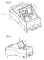
- Fig. 1 shows a terminal unit 1 with a casing 2 and a cover 3. Between the casing 2 and the cover 3 there is an aperture 4 for feeding in a cable.
- a receiving aperture 5 with a terminal module 6 inserted in it is provided in the cover 3.
- Two sockets 7 are provided in the terminal module 6, the right-hand socket 7 being covered for example with a hinged cover 8.
- the terminal module 6 is fixed in the cover 3 by a screw 9.
- the screw 9 is in the form of a lifting screw which may be used to displace the terminal module 6 and release that module.
- the terminal module 6 may be moved from a pre-latching position to a contact position by means of the screw 9.
- Fig. 2 shows the terminal unit 1 before the terminal module 6 is inserted in the receiving aperture 5.
- the cover 3 has screw thread 48 for screwing the module 6 onto the cover 3.
- Fig. 3 shows the terminal module 6, which has a socket casing 10 and a printed circuit board 11.
- the printed circuit board 11 has conductors 12 which are electrically connected to contacts of the sockets 7 and arranged on the underside of the printed circuit board 11.
- the sockets 7 are designed for example for connectors of telephone cables or connectors of network cables.
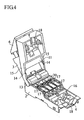
- Fig. 4 shows the terminal unit 1 with a cover 3 swung open.
- the cover 3 is supported on the casing 2 so that it can be swivelled by means of a hinge 13.
- the terminal module 6 is pre-mounted in the cover 3 and not fully inserted in the receiving aperture 5.
- the printed circuit board 11 is guided laterally in slots 14 in side walls 15 of the cover 3.
- a retaining plate 16 is arranged in the casing 2 and screwed to a base of the casing 2 by a screw connection.
- a plurality of contact members 17 are arranged on the retaining plate 16.
- the aperture 4 is bounded partly by the casing 2 and partly by the cover 3.
- a strain relief section 18 and a shielding contact means 19 are arranged in the aperture 4.
- the function of the strain relief section 18 is to clamp an insulating jacket of the cable.
- the shielding contact means 19 is produced from an electrically conductive material and its function is to make electrical contact with a shield of a cable.
- the casing 2 and cover 3 are preferably produced from an electrically conductive material, particularly a die-cast material, so shielding against electromagnetic radiation is achieved.
- the retaining plate 16 is preferably made of an insulative material or a material which shields against electromagnetic radiation.
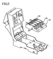
- Fig. 5 shows the terminal unit 1 swung open with the retaining plate 16 before being mounted in the casing 2.
- the retaining plate 16 is supported in the casing 2 by a floating mounting so that manufacturing tolerances can be compensated.
- the floating mounting is shown in the form of wedge-shaped recesses 20 and wedge-shaped segments 21, the recesses 20 being formed in side walls of the retaining plate 16 and the segments 21 in side walls of the casing 2.
- the floating mounting is advantageous because the printed circuit board 11 is slid in the assembled state into a receiving chamber 39 formed by the contact members 17. Accurate alignment of the contact members 17 with the printed circuit board 11 is necessary in order to make good contact with the printed circuit board 11.
- the compensating mounting enables the retaining plate 16 to be both tilted and displaced in the longitudinal direction.
- the tilting axis is defined by the seating surface of the wedge-shaped segments 21 on which the retaining plate 16 rests in the wedge-shaped recesses 20.
- Fig. 6 shows the retaining plate 16 with four contact members 17, the right-hand contact member 17 being in an open position.
- the four contact members 17 are juxtaposed, and in this special embodiment each contact member 17 is held on the retaining plate 16 so that it can swivel by means of a hinge pin.
- the retaining plate 16 may also be integral with the casing 2.
- Partition walls 23 are arranged between the contact members 17 and, preferably with the retaining plate 16, are made of a material which shields against electromagnetic radiation.
- a retaining cage 24 for receiving and holding electrical leads 25 is in each case arranged between the partition walls 23. In the embodiment illustrated two juxtaposed and separated channels 26 are provided in the retaining cage 24.
- the retaining cage 24 is made of an insulative material.
- the channels 26 are open at the front.
- Two contact apertures 27 are formed at the top of the retaining cage 24.
- the contact apertures 27 of the two channels 26 are offset from each other in the longitudinal direction of the channels 26.
- At least the top of the retaining cage 24 is preferably made of a transparent material.
- Each channel 26 has a stop face opposite the front apertures. For correct assembly the electrical leads 25 are inserted through the apertures of the conductor channels 26 as far as the stop face.
- the contact member 17 has two contacts 28, 29.
- the two contacts 28, 29 have contact regions 30, 31 in the form of insulation displacement connecting devices arranged perpendicular to the underside of the contact member 17.
- the contact regions 30, 31 are arranged in such a way that when the contact member 17 is swivelled the first and second contact areas 30, 31 engage in the associated contact aperture 27, establishing an electrical connection with the electrical leads 25 inserted in the channels 26.
- the contact member 17 is produced from an insulative material into which the contacts 28, 29 are inserted.
- the contact member 17 extends in the longitudinal direction to beyond the retaining cage 24 in the direction of the electrical leads 25.
- the contact member 17 has two brackets 32 arranged opposite each other on longitudinal sides of the member 17.
- the function of the brackets 32 is to hold the two leads 25 laterally and preferably press them together.
- Brackets 32 are long enough for their ends to engage in associated apertures 33 in the retaining plate 16 when the contact member 17 is in the contact position.
- the brackets 32 have a diameter which widens from the ends to the center of the contact member 17, so that an upwardly tapering surface is formed in cross-section by the two brackets 32.
- the brackets 32 each have a latching lug on the inside, which engage in corresponding latching recesses in the apertures 33. In this way the contact members 17 are held securely in the contact position, i.e. in the latched condition.
- the contact members 17 have an actuating surface 34 at the top and a gripping surface 35 at the front end towards the electrical leads 25.
- the contact member 17 can easily be pushed from the open position to the contact position by an operator by means of the actuating surface 34.
- the force required to contact the electrical leads 25 can easily be applied by means of the relatively large actuating surface 34. If insulation displacement connecting devices are used the insulation of the leads 25 has to be undone.
- the contact member 17 can be opened from the contact position in a simple manner by means of the gripping surface 35, which can be actuated with a tool or a finger.
- the contact members 17 have first seating surfaces 36 and second seating surfaces 37 at the end opposite the gripping surface 35.
- the first seating surface 36 is arranged on the top of the contact member 17.
- the second seating surface 37 is located on the inside of a U-shaped end piece 38 of the contact member.
- the first and second seating surfaces 36, 37 bound a receiving chamber 39.
- the first and second seating surfaces 36, 37 of the four contact members 17 are arranged parallel with each other and bound the receiving chamber 39 for receiving an edge region of the printed circuit board 11.
- the partition walls 23 are preferably bevelled in the region of the receiving chamber 39 to match the inclination of the first seating surfaces 36, and the bevelled surface 49 of the partition walls 23 forms a further seating surface for the printed circuit board 11.
- Fig. 7 is a perspective view of a contact member 17 with a second contact 29 in the form of a spring contact.
- the upwardly tapering surface 50 between the two brackets 32 is also clearly recognisable in Fig. 7. It is formed between the brackets 32 and is preferably responsible for clamped retention of the leads 25.
- the contact member 17 has an S shape in the rear region and is bent down under the receiving chamber 39 forming a space 41.
- the contact member 17 has a second hinge pin 40, about which the contact member 17 is supported pivotably with the retaining plate 16.
- the space 41 into which a U-shaped contact piece 42 of the second contact 29 can pass resiliently when the printed circuit board 11 is inserted is formed under the receiving chamber 39.
- Fig. 8 shows an embodiment of the first and second contacts 28, 29 in the form of a spring contact 43, in a perspective view.
- the spring contact 43 has an insulation displacement connecting device 44 for making electrical contact with the electrical lead 25.
- the spring contact 43 is in the form of a U-shaped contact piece 42, and a second end piece 45 engages under a seating surface 46 of the contact member 17.
- the contact piece 42 is thereby pre-tensioned. It has an upwardly curved contact surface 47, provided to make electrical contact with a contact member 17 of the printed circuit board 11.
- the U shape of the contact piece 42 gives high resilience despite the compact shape of the spring contact 43, so secure electric contact is obtained between the contact surface 47 and a conductor 12 of the printed circuit board 11.
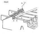
- Fig. 9 shows a fragment of a terminal unit 1 with the terminal module 6 in the pre-mounted condition as illustrated in Fig. 10.
- the receiving chamber 39 bounded by the first and second seating surfaces 36, 37 is arranged parallel with the alignment of the printed circuit board 11.
- an end piece 22 of the printed circuit board 11 slides into the receiving chamber 39 and electric contact is made between the contacts 28, 29 of the contact members 17 and the conductors 12 of the printed circuit board 11.
- the conductors 12 are located on the underside of the printed circuit board 11.
- the printed circuit board 11 is pressed against the second seating surface 37 by the spring tension of the contacts 28, 29.
Landscapes
- Coupling Device And Connection With Printed Circuit (AREA)
- Multi-Conductor Connections (AREA)
- Connections By Means Of Piercing Elements, Nuts, Or Screws (AREA)
Abstract
Description
Claims (12)
- A terminal unit (1) for putting an electrical lead (25) in contact with a printed circuit board (11), comprising a casing (2) with a retaining cage (24) for the electrical lead (25), and a contact (28, 29) for contacting the electrical lead (25),
characterised in that the contact (28, 29) is held in a contact member (17), that the contact member (17) is held movably on the casing (2), that the contact member (17) can be moved from an open position to a contact position, the contact (28, 29) being electrically contacted with the electrical lead (25), that the contact member (17) has a receiving chamber (39) to receive the printed circuit board (11), and that the contact (28, 29) is guided into the receiving chamber (39) for electric contacting with a conductor (12) of the printed circuit board (11). - A terminal unit according to claim 1, characterised in that the contact member (17) is held so that it can swivel about a hinge pin (40), and the contact (28, 29) of the contact member (17) can be swivelled into the retaining cage (24) for contacting with the electrical lead (25).
- A terminal unit according to claim 1 or 2, characterised in that the contact member (17) extends beyond the retaining cage (24) in the contact position, that the contact member (17) has two laterally arranged brackets (32), that the brackets (32) engage in two apertures in a retaining plate (16) in the contact position of the contact member (17), that the two brackets (32) are provided to hold and/or clamp the electrical lead (25).
- A terminal unit according to any of claims 1 to 3, characterised in that the contact member (17) has an actuating surface (34) on top, provided for swivelling the contact member (17).
- A terminal unit according to any of claims 1 to 4, characterised in that two contacts (28, 29) are arranged in a contact member (17), that the two contacts (28, 29) have contact regions (30, 31) with which electric contact is made with associated electrical leads (25), and that the contact regions (30, 31) are arranged offset from each other in the longitudinal direction of the electrical leads (25).
- A terminal unit according to any of claims 1 to 5, characterised in that a plurality of contact members (17) are juxtaposed in the casing, that partition walls (23) are arranged between the contact members (17), and that the partition walls (23) are produced from a material which shields electromagnetic radiation.
- A terminal unit according to any of claims 1 to 6, characterised in that the retaining cage (24) has a front aperture for guiding in an electrical lead (25), that the retaining cage (24) has a contact aperture (27) for guiding in the contact (28, 29), that the retaining cage (24) is made of a transparent material at least at the top, which is assigned to the contact member (17).
- A terminal unit according to any of claims 1 to 7, characterised in that the receiving chamber (39) is formed by two seating surfaces (36, 37) of the contact member (17), and that an end piece (38) of the contact member (17) is arranged in the receiving chamber (39), that a space (41) adjoining the receiving chamber (39) is formed in the contact member (17), into which the contact piece (42) recedes when the end piece (22) of the printed circuit board (11) is introduced.
- A terminal unit according to any of claims 1 to 8, characterised in that the contact member (17) is held on a retaining plate (16), and that the retaining plate (16) is held in a compensating mounting (20, 21) in the casing (2), which enables a tilting movement of the retaining plate (16) and/or a displacement of the retaining plate (16).
- A terminal unit according to any of claims 1 to 9, characterised in that the casing (2) has a cover (3), that a receiving aperture (5) for the printed circuit board (11) and a socket (7) are provided in the cover (3), that the printed circuit board (11) is held displaceably by slots (14) in the cover (3), and that the printed circuit board 11 can be inserted in the receiving chamber (39) of the contact member (17).
- A terminal unit according to claim 10, characterised in that the cover (3) is mounted pivotably on the casing (2) and can be swivelled from an open position to a closed position in which the printed circuit board (11) is aligned with the receiving chamber (39).
- A terminal unit according to claim 10, characterised in that the printed circuit board (11) is held displaceably to the cover, that the printed circuit board (11) is in a standby position in the open position of the cover (3), and that the printed circuit board (11) can be moved into a contact position in the closed position of the cover (3), the printed circuit board (11) being slid into the receiving chamber (39), and electric contact being made between the printed circuit board (11) and the contact member (17).
Priority Applications (1)
| Application Number | Priority Date | Filing Date | Title |
|---|---|---|---|
| EP04026526.6A EP1531523B1 (en) | 2003-11-13 | 2004-11-09 | Lead connector for circuit board |
Applications Claiming Priority (3)
| Application Number | Priority Date | Filing Date | Title |
|---|---|---|---|
| EP03025941 | 2003-11-13 | ||
| EP03025941 | 2003-11-13 | ||
| EP04026526.6A EP1531523B1 (en) | 2003-11-13 | 2004-11-09 | Lead connector for circuit board |
Publications (3)
| Publication Number | Publication Date |
|---|---|
| EP1531523A2 true EP1531523A2 (en) | 2005-05-18 |
| EP1531523A3 EP1531523A3 (en) | 2006-03-01 |
| EP1531523B1 EP1531523B1 (en) | 2017-03-01 |
Family
ID=34626374
Family Applications (1)
| Application Number | Title | Priority Date | Filing Date |
|---|---|---|---|
| EP04026526.6A Expired - Lifetime EP1531523B1 (en) | 2003-11-13 | 2004-11-09 | Lead connector for circuit board |
Country Status (3)
| Country | Link |
|---|---|
| US (1) | US7134904B2 (en) |
| EP (1) | EP1531523B1 (en) |
| JP (1) | JP4614270B2 (en) |
Cited By (1)
| Publication number | Priority date | Publication date | Assignee | Title |
|---|---|---|---|---|
| DE202021103278U1 (en) | 2021-06-18 | 2022-09-22 | Electro Terminal GmbH & Co. KG | clamp |
Families Citing this family (9)
| Publication number | Priority date | Publication date | Assignee | Title |
|---|---|---|---|---|
| DE102006039799B3 (en) * | 2006-08-24 | 2007-11-22 | Tyco Electronics Amp Gmbh | Electrical plug, has retainer with holder holding conductor units of cable, and housing units and contact units arranged opposite to retainer, where contact units are connected with conductor units when housing units are in closed position |
| US7281941B1 (en) * | 2007-04-04 | 2007-10-16 | Aslan Industries, Corporation | Stripping and contact device for an insulation displacement connector |
| DE102008027512B4 (en) * | 2008-06-10 | 2010-07-01 | Tyco Electronics Amp Gmbh | Electric plug |
| DE102008057554B3 (en) * | 2008-11-15 | 2010-04-22 | Tyco Electronics Amp Gmbh | Electrical connector with stranded conductor |
| US8430689B2 (en) * | 2011-07-22 | 2013-04-30 | Tyco Electronics Corporation | Electrical connector |
| US9379500B2 (en) | 2013-03-11 | 2016-06-28 | Panduit Corp. | Front sled assemblies for communication jacks and communication jacks having front sled assemblies |
| US9640924B2 (en) | 2014-05-22 | 2017-05-02 | Panduit Corp. | Communication plug |
| WO2017201177A1 (en) | 2016-05-20 | 2017-11-23 | Communications Systems, Inc. | Toolless communications jack |
| US11881669B2 (en) | 2021-05-28 | 2024-01-23 | Electro Terminal Gmbh & Co Kg | Terminal |
Family Cites Families (12)
| Publication number | Priority date | Publication date | Assignee | Title |
|---|---|---|---|---|
| AU5574573A (en) * | 1972-05-30 | 1974-11-21 | Amp Inc | Electrical contact elements and connectors electrical contact elements and connectors |
| US4891019A (en) * | 1989-03-03 | 1990-01-02 | Amp Incorporated | Electrical connector for interconnecting a printed circuit board to a ribbon cable |
| AU678743B2 (en) * | 1995-03-31 | 1997-06-05 | Matsushita Electric Works Ltd. | Lever modular jack electrical connector |
| US5667402A (en) * | 1995-12-15 | 1997-09-16 | Denovich; Sam | Wire carrier for electrical connector modular |
| US6246749B1 (en) | 1997-01-31 | 2001-06-12 | The Whitaker Corporation | Network interface unit and module |
| DE19753076C1 (en) * | 1997-11-29 | 1999-08-19 | Lumberg Karl Gmbh & Co | Electrical connector, esp. series connector |
| USRE38519E1 (en) * | 1998-08-24 | 2004-05-18 | Panduit Corp. | Low crosstalk modular communication connector |
| US5947761A (en) * | 1998-09-29 | 1999-09-07 | The Whitaker Corporation | Electrical connector with pivoting wire fixture |
| JP2001203031A (en) * | 2000-01-20 | 2001-07-27 | Sumitomo Wiring Syst Ltd | connector |
| JP2001257039A (en) * | 2000-02-21 | 2001-09-21 | Tyco Electronics Amp Espanola Sa | Electrical connector |
| EP1128488B1 (en) * | 2000-02-21 | 2015-02-11 | Tyco Electronics AMP España S.A. | Electrical connector for high speed signal transmission |
| US6893280B2 (en) * | 2003-04-30 | 2005-05-17 | Tyco Electronics Corporation | Toggle type telecommunications terminal blocks |
-
2004
- 2004-11-09 EP EP04026526.6A patent/EP1531523B1/en not_active Expired - Lifetime
- 2004-11-12 JP JP2004329594A patent/JP4614270B2/en not_active Expired - Lifetime
- 2004-11-12 US US10/986,980 patent/US7134904B2/en not_active Expired - Lifetime
Cited By (1)
| Publication number | Priority date | Publication date | Assignee | Title |
|---|---|---|---|---|
| DE202021103278U1 (en) | 2021-06-18 | 2022-09-22 | Electro Terminal GmbH & Co. KG | clamp |
Also Published As
| Publication number | Publication date |
|---|---|
| JP4614270B2 (en) | 2011-01-19 |
| EP1531523A3 (en) | 2006-03-01 |
| US7134904B2 (en) | 2006-11-14 |
| JP2005150115A (en) | 2005-06-09 |
| EP1531523B1 (en) | 2017-03-01 |
| US20050124206A1 (en) | 2005-06-09 |
Similar Documents
| Publication | Publication Date | Title |
|---|---|---|
| CN102246360B (en) | electrical connection plug | |
| US4340270A (en) | Electrical terminal unit | |
| CN102801030B (en) | Cable connector | |
| CN100470932C (en) | Modular Telecom Connector Jacks and Termination Assemblies | |
| US12021339B2 (en) | Spring terminal for conductor | |
| KR20140022736A (en) | Modular plug | |
| WO1988004482A1 (en) | Shielded electrical connector having an insulating cover on the shielding member | |
| US5061198A (en) | Electrical connector system | |
| CA2135443A1 (en) | Electrical connector with cable shield ground clip | |
| US5564940A (en) | Electrical connector having a conductor holding block | |
| US7134904B2 (en) | Terminal unit for putting a lead into contact with a printed circuit board | |
| US4577920A (en) | Electrical assembly with cable guiding member | |
| US5681180A (en) | Conductor holding block for an electrical connector | |
| US6887094B2 (en) | Shielded connection arrangement for data transfer | |
| EP0653804B1 (en) | Electrical connector having a conductor holding block | |
| US7074071B2 (en) | Plug connector | |
| US6007367A (en) | Apparatus for connecting cable cores | |
| CN118554202A (en) | Branch connector and contact and pivoting housing part for a branch connector | |
| CN110611185B (en) | Electric connector combination | |
| RU2811757C1 (en) | Spring clamp terminal | |
| KR20010030184A (en) | Electric connector | |
| JPH11353955A (en) | Flat cable terminal structure and connector for connecting it | |
| EP1037313B1 (en) | Female connector with strain relief device and process for mounting this connector on pcb | |
| EP1403966B1 (en) | Shielded connection arrangement for data transfer | |
| EP0454278B1 (en) | Electrical connector for use on a circuit board |
Legal Events
| Date | Code | Title | Description |
|---|---|---|---|
| PUAI | Public reference made under article 153(3) epc to a published international application that has entered the european phase |
Free format text: ORIGINAL CODE: 0009012 |
|
| AK | Designated contracting states |
Kind code of ref document: A2 Designated state(s): AT BE BG CH CY CZ DE DK EE ES FI FR GB GR HU IE IS IT LI LU MC NL PL PT RO SE SI SK TR |
|
| AX | Request for extension of the european patent |
Extension state: AL HR LT LV MK YU |
|
| PUAL | Search report despatched |
Free format text: ORIGINAL CODE: 0009013 |
|
| AK | Designated contracting states |
Kind code of ref document: A3 Designated state(s): AT BE BG CH CY CZ DE DK EE ES FI FR GB GR HU IE IS IT LI LU MC NL PL PT RO SE SI SK TR |
|
| AX | Request for extension of the european patent |
Extension state: AL HR LT LV MK YU |
|
| 17P | Request for examination filed |
Effective date: 20060526 |
|
| AKX | Designation fees paid |
Designated state(s): AT BE BG CH CY CZ DE DK EE ES FI FR GB GR HU IE IS IT LI LU MC NL PL PT RO SE SI SK TR |
|
| RAP1 | Party data changed (applicant data changed or rights of an application transferred) |
Owner name: TE CONNECTIVITY GERMANY GMBH |
|
| REG | Reference to a national code |
Ref country code: DE Ref legal event code: R079 Ref document number: 602004050818 Country of ref document: DE Free format text: PREVIOUS MAIN CLASS: H01R0012040000 Ipc: H01R0012520000 |
|
| RIC1 | Information provided on ipc code assigned before grant |
Ipc: H01R 12/52 20110101AFI20160720BHEP |
|
| GRAP | Despatch of communication of intention to grant a patent |
Free format text: ORIGINAL CODE: EPIDOSNIGR1 |
|
| INTG | Intention to grant announced |
Effective date: 20160912 |
|
| GRAS | Grant fee paid |
Free format text: ORIGINAL CODE: EPIDOSNIGR3 |
|
| GRAA | (expected) grant |
Free format text: ORIGINAL CODE: 0009210 |
|
| AK | Designated contracting states |
Kind code of ref document: B1 Designated state(s): AT BE BG CH CY CZ DE DK EE ES FI FR GB GR HU IE IS IT LI LU MC NL PL PT RO SE SI SK TR |
|
| REG | Reference to a national code |
Ref country code: GB Ref legal event code: FG4D |
|
| REG | Reference to a national code |
Ref country code: CH Ref legal event code: EP Ref country code: AT Ref legal event code: REF Ref document number: 872323 Country of ref document: AT Kind code of ref document: T Effective date: 20170315 |
|
| REG | Reference to a national code |
Ref country code: IE Ref legal event code: FG4D |
|
| REG | Reference to a national code |
Ref country code: DE Ref legal event code: R096 Ref document number: 602004050818 Country of ref document: DE |
|
| REG | Reference to a national code |
Ref country code: NL Ref legal event code: MP Effective date: 20170301 |
|
| REG | Reference to a national code |
Ref country code: AT Ref legal event code: MK05 Ref document number: 872323 Country of ref document: AT Kind code of ref document: T Effective date: 20170301 |
|
| PG25 | Lapsed in a contracting state [announced via postgrant information from national office to epo] |
Ref country code: GR Free format text: LAPSE BECAUSE OF FAILURE TO SUBMIT A TRANSLATION OF THE DESCRIPTION OR TO PAY THE FEE WITHIN THE PRESCRIBED TIME-LIMIT Effective date: 20170602 Ref country code: FI Free format text: LAPSE BECAUSE OF FAILURE TO SUBMIT A TRANSLATION OF THE DESCRIPTION OR TO PAY THE FEE WITHIN THE PRESCRIBED TIME-LIMIT Effective date: 20170301 |
|
| PG25 | Lapsed in a contracting state [announced via postgrant information from national office to epo] |
Ref country code: BG Free format text: LAPSE BECAUSE OF FAILURE TO SUBMIT A TRANSLATION OF THE DESCRIPTION OR TO PAY THE FEE WITHIN THE PRESCRIBED TIME-LIMIT Effective date: 20170601 Ref country code: ES Free format text: LAPSE BECAUSE OF FAILURE TO SUBMIT A TRANSLATION OF THE DESCRIPTION OR TO PAY THE FEE WITHIN THE PRESCRIBED TIME-LIMIT Effective date: 20170301 Ref country code: SE Free format text: LAPSE BECAUSE OF FAILURE TO SUBMIT A TRANSLATION OF THE DESCRIPTION OR TO PAY THE FEE WITHIN THE PRESCRIBED TIME-LIMIT Effective date: 20170301 Ref country code: AT Free format text: LAPSE BECAUSE OF FAILURE TO SUBMIT A TRANSLATION OF THE DESCRIPTION OR TO PAY THE FEE WITHIN THE PRESCRIBED TIME-LIMIT Effective date: 20170301 |
|
| PG25 | Lapsed in a contracting state [announced via postgrant information from national office to epo] |
Ref country code: NL Free format text: LAPSE BECAUSE OF FAILURE TO SUBMIT A TRANSLATION OF THE DESCRIPTION OR TO PAY THE FEE WITHIN THE PRESCRIBED TIME-LIMIT Effective date: 20170301 |
|
| PG25 | Lapsed in a contracting state [announced via postgrant information from national office to epo] |
Ref country code: IT Free format text: LAPSE BECAUSE OF FAILURE TO SUBMIT A TRANSLATION OF THE DESCRIPTION OR TO PAY THE FEE WITHIN THE PRESCRIBED TIME-LIMIT Effective date: 20170301 Ref country code: SK Free format text: LAPSE BECAUSE OF FAILURE TO SUBMIT A TRANSLATION OF THE DESCRIPTION OR TO PAY THE FEE WITHIN THE PRESCRIBED TIME-LIMIT Effective date: 20170301 Ref country code: EE Free format text: LAPSE BECAUSE OF FAILURE TO SUBMIT A TRANSLATION OF THE DESCRIPTION OR TO PAY THE FEE WITHIN THE PRESCRIBED TIME-LIMIT Effective date: 20170301 Ref country code: RO Free format text: LAPSE BECAUSE OF FAILURE TO SUBMIT A TRANSLATION OF THE DESCRIPTION OR TO PAY THE FEE WITHIN THE PRESCRIBED TIME-LIMIT Effective date: 20170301 Ref country code: CZ Free format text: LAPSE BECAUSE OF FAILURE TO SUBMIT A TRANSLATION OF THE DESCRIPTION OR TO PAY THE FEE WITHIN THE PRESCRIBED TIME-LIMIT Effective date: 20170301 |
|
| REG | Reference to a national code |
Ref country code: FR Ref legal event code: PLFP Year of fee payment: 14 |
|
| PG25 | Lapsed in a contracting state [announced via postgrant information from national office to epo] |
Ref country code: PT Free format text: LAPSE BECAUSE OF FAILURE TO SUBMIT A TRANSLATION OF THE DESCRIPTION OR TO PAY THE FEE WITHIN THE PRESCRIBED TIME-LIMIT Effective date: 20170703 Ref country code: PL Free format text: LAPSE BECAUSE OF FAILURE TO SUBMIT A TRANSLATION OF THE DESCRIPTION OR TO PAY THE FEE WITHIN THE PRESCRIBED TIME-LIMIT Effective date: 20170301 Ref country code: IS Free format text: LAPSE BECAUSE OF FAILURE TO SUBMIT A TRANSLATION OF THE DESCRIPTION OR TO PAY THE FEE WITHIN THE PRESCRIBED TIME-LIMIT Effective date: 20170701 |
|
| REG | Reference to a national code |
Ref country code: DE Ref legal event code: R097 Ref document number: 602004050818 Country of ref document: DE |
|
| PLBE | No opposition filed within time limit |
Free format text: ORIGINAL CODE: 0009261 |
|
| STAA | Information on the status of an ep patent application or granted ep patent |
Free format text: STATUS: NO OPPOSITION FILED WITHIN TIME LIMIT |
|
| PG25 | Lapsed in a contracting state [announced via postgrant information from national office to epo] |
Ref country code: DK Free format text: LAPSE BECAUSE OF FAILURE TO SUBMIT A TRANSLATION OF THE DESCRIPTION OR TO PAY THE FEE WITHIN THE PRESCRIBED TIME-LIMIT Effective date: 20170301 |
|
| 26N | No opposition filed |
Effective date: 20171204 |
|
| PG25 | Lapsed in a contracting state [announced via postgrant information from national office to epo] |
Ref country code: SI Free format text: LAPSE BECAUSE OF FAILURE TO SUBMIT A TRANSLATION OF THE DESCRIPTION OR TO PAY THE FEE WITHIN THE PRESCRIBED TIME-LIMIT Effective date: 20170301 |
|
| PG25 | Lapsed in a contracting state [announced via postgrant information from national office to epo] |
Ref country code: MC Free format text: LAPSE BECAUSE OF FAILURE TO SUBMIT A TRANSLATION OF THE DESCRIPTION OR TO PAY THE FEE WITHIN THE PRESCRIBED TIME-LIMIT Effective date: 20170301 |
|
| PG25 | Lapsed in a contracting state [announced via postgrant information from national office to epo] |
Ref country code: CH Free format text: LAPSE BECAUSE OF NON-PAYMENT OF DUE FEES Effective date: 20171130 Ref country code: LI Free format text: LAPSE BECAUSE OF NON-PAYMENT OF DUE FEES Effective date: 20171130 |
|
| PG25 | Lapsed in a contracting state [announced via postgrant information from national office to epo] |
Ref country code: LU Free format text: LAPSE BECAUSE OF NON-PAYMENT OF DUE FEES Effective date: 20171109 |
|
| REG | Reference to a national code |
Ref country code: BE Ref legal event code: MM Effective date: 20171130 |
|
| REG | Reference to a national code |
Ref country code: IE Ref legal event code: MM4A |
|
| REG | Reference to a national code |
Ref country code: FR Ref legal event code: PLFP Year of fee payment: 15 |
|
| PG25 | Lapsed in a contracting state [announced via postgrant information from national office to epo] |
Ref country code: IE Free format text: LAPSE BECAUSE OF NON-PAYMENT OF DUE FEES Effective date: 20171109 |
|
| PG25 | Lapsed in a contracting state [announced via postgrant information from national office to epo] |
Ref country code: BE Free format text: LAPSE BECAUSE OF NON-PAYMENT OF DUE FEES Effective date: 20171130 |
|
| PG25 | Lapsed in a contracting state [announced via postgrant information from national office to epo] |
Ref country code: HU Free format text: LAPSE BECAUSE OF FAILURE TO SUBMIT A TRANSLATION OF THE DESCRIPTION OR TO PAY THE FEE WITHIN THE PRESCRIBED TIME-LIMIT; INVALID AB INITIO Effective date: 20041109 |
|
| PG25 | Lapsed in a contracting state [announced via postgrant information from national office to epo] |
Ref country code: CY Free format text: LAPSE BECAUSE OF NON-PAYMENT OF DUE FEES Effective date: 20170301 |
|
| PG25 | Lapsed in a contracting state [announced via postgrant information from national office to epo] |
Ref country code: TR Free format text: LAPSE BECAUSE OF FAILURE TO SUBMIT A TRANSLATION OF THE DESCRIPTION OR TO PAY THE FEE WITHIN THE PRESCRIBED TIME-LIMIT Effective date: 20170301 |
|
| PGFP | Annual fee paid to national office [announced via postgrant information from national office to epo] |
Ref country code: GB Payment date: 20230921 Year of fee payment: 20 |
|
| PGFP | Annual fee paid to national office [announced via postgrant information from national office to epo] |
Ref country code: FR Payment date: 20230911 Year of fee payment: 20 |
|
| PGFP | Annual fee paid to national office [announced via postgrant information from national office to epo] |
Ref country code: DE Payment date: 20230912 Year of fee payment: 20 |
|
| REG | Reference to a national code |
Ref country code: DE Ref legal event code: R071 Ref document number: 602004050818 Country of ref document: DE |
|
| REG | Reference to a national code |
Ref country code: GB Ref legal event code: PE20 Expiry date: 20241108 |
|
| PG25 | Lapsed in a contracting state [announced via postgrant information from national office to epo] |
Ref country code: GB Free format text: LAPSE BECAUSE OF EXPIRATION OF PROTECTION Effective date: 20241108 |
|
| PG25 | Lapsed in a contracting state [announced via postgrant information from national office to epo] |
Ref country code: GB Free format text: LAPSE BECAUSE OF EXPIRATION OF PROTECTION Effective date: 20241108 |