EP1530238A1 - Dispositif de détection de rayonnements infrarouges à détecteurs bolométriques - Google Patents
Dispositif de détection de rayonnements infrarouges à détecteurs bolométriques Download PDFInfo
- Publication number
- EP1530238A1 EP1530238A1 EP04300759A EP04300759A EP1530238A1 EP 1530238 A1 EP1530238 A1 EP 1530238A1 EP 04300759 A EP04300759 A EP 04300759A EP 04300759 A EP04300759 A EP 04300759A EP 1530238 A1 EP1530238 A1 EP 1530238A1
- Authority
- EP
- European Patent Office
- Prior art keywords
- detectors
- bolometric
- connection
- detector
- circuit
- Prior art date
- Legal status (The legal status is an assumption and is not a legal conclusion. Google has not performed a legal analysis and makes no representation as to the accuracy of the status listed.)
- Granted
Links
- 230000005855 radiation Effects 0.000 title description 9
- 239000011159 matrix material Substances 0.000 claims abstract description 27
- 239000000463 material Substances 0.000 claims abstract description 16
- 238000001514 detection method Methods 0.000 claims description 13
- 238000009413 insulation Methods 0.000 claims description 6
- 239000012528 membrane Substances 0.000 abstract description 4
- 238000000034 method Methods 0.000 description 10
- 230000008901 benefit Effects 0.000 description 5
- 238000010276 construction Methods 0.000 description 4
- 230000010354 integration Effects 0.000 description 4
- 230000003071 parasitic effect Effects 0.000 description 4
- 230000004913 activation Effects 0.000 description 3
- 230000007547 defect Effects 0.000 description 3
- 230000000694 effects Effects 0.000 description 3
- 230000005284 excitation Effects 0.000 description 3
- 238000003384 imaging method Methods 0.000 description 3
- 230000006872 improvement Effects 0.000 description 3
- IJGRMHOSHXDMSA-UHFFFAOYSA-N Atomic nitrogen Chemical compound N#N IJGRMHOSHXDMSA-UHFFFAOYSA-N 0.000 description 2
- XUIMIQQOPSSXEZ-UHFFFAOYSA-N Silicon Chemical compound [Si] XUIMIQQOPSSXEZ-UHFFFAOYSA-N 0.000 description 2
- XHCLAFWTIXFWPH-UHFFFAOYSA-N [O-2].[O-2].[O-2].[O-2].[O-2].[V+5].[V+5] Chemical compound [O-2].[O-2].[O-2].[O-2].[O-2].[V+5].[V+5] XHCLAFWTIXFWPH-UHFFFAOYSA-N 0.000 description 2
- 238000010521 absorption reaction Methods 0.000 description 2
- 230000009471 action Effects 0.000 description 2
- 238000012937 correction Methods 0.000 description 2
- 238000003331 infrared imaging Methods 0.000 description 2
- 238000002955 isolation Methods 0.000 description 2
- 238000004519 manufacturing process Methods 0.000 description 2
- 230000008520 organization Effects 0.000 description 2
- 229910052710 silicon Inorganic materials 0.000 description 2
- 239000010703 silicon Substances 0.000 description 2
- 239000000758 substrate Substances 0.000 description 2
- 238000004861 thermometry Methods 0.000 description 2
- OKTJSMMVPCPJKN-UHFFFAOYSA-N Carbon Chemical compound [C] OKTJSMMVPCPJKN-UHFFFAOYSA-N 0.000 description 1
- 241001415961 Gaviidae Species 0.000 description 1
- 241001080024 Telles Species 0.000 description 1
- 230000003213 activating effect Effects 0.000 description 1
- 229910021417 amorphous silicon Inorganic materials 0.000 description 1
- 238000003491 array Methods 0.000 description 1
- 229910052799 carbon Inorganic materials 0.000 description 1
- 238000006243 chemical reaction Methods 0.000 description 1
- 238000007796 conventional method Methods 0.000 description 1
- 238000001816 cooling Methods 0.000 description 1
- 238000013461 design Methods 0.000 description 1
- 229910052732 germanium Inorganic materials 0.000 description 1
- GNPVGFCGXDBREM-UHFFFAOYSA-N germanium atom Chemical compound [Ge] GNPVGFCGXDBREM-UHFFFAOYSA-N 0.000 description 1
- 238000010438 heat treatment Methods 0.000 description 1
- 230000001939 inductive effect Effects 0.000 description 1
- 239000007788 liquid Substances 0.000 description 1
- 229910052751 metal Inorganic materials 0.000 description 1
- 239000002184 metal Substances 0.000 description 1
- 238000004377 microelectronic Methods 0.000 description 1
- 201000009240 nasopharyngitis Diseases 0.000 description 1
- 229910052757 nitrogen Inorganic materials 0.000 description 1
- 238000004806 packaging method and process Methods 0.000 description 1
- 230000010287 polarization Effects 0.000 description 1
- 238000007781 pre-processing Methods 0.000 description 1
- 238000002203 pretreatment Methods 0.000 description 1
- 210000001525 retina Anatomy 0.000 description 1
- 230000003068 static effect Effects 0.000 description 1
- 230000001052 transient effect Effects 0.000 description 1
- 229910001935 vanadium oxide Inorganic materials 0.000 description 1
Images


Classifications
-
- H—ELECTRICITY
- H10—SEMICONDUCTOR DEVICES; ELECTRIC SOLID-STATE DEVICES NOT OTHERWISE PROVIDED FOR
- H10F—INORGANIC SEMICONDUCTOR DEVICES SENSITIVE TO INFRARED RADIATION, LIGHT, ELECTROMAGNETIC RADIATION OF SHORTER WAVELENGTH OR CORPUSCULAR RADIATION
- H10F39/00—Integrated devices, or assemblies of multiple devices, comprising at least one element covered by group H10F30/00, e.g. radiation detectors comprising photodiode arrays
- H10F39/10—Integrated devices
-
- G—PHYSICS
- G01—MEASURING; TESTING
- G01J—MEASUREMENT OF INTENSITY, VELOCITY, SPECTRAL CONTENT, POLARISATION, PHASE OR PULSE CHARACTERISTICS OF INFRARED, VISIBLE OR ULTRAVIOLET LIGHT; COLORIMETRY; RADIATION PYROMETRY
- G01J5/00—Radiation pyrometry, e.g. infrared or optical thermometry
- G01J5/10—Radiation pyrometry, e.g. infrared or optical thermometry using electric radiation detectors
- G01J5/20—Radiation pyrometry, e.g. infrared or optical thermometry using electric radiation detectors using resistors, thermistors or semiconductors sensitive to radiation, e.g. photoconductive devices
-
- H—ELECTRICITY
- H10—SEMICONDUCTOR DEVICES; ELECTRIC SOLID-STATE DEVICES NOT OTHERWISE PROVIDED FOR
- H10F—INORGANIC SEMICONDUCTOR DEVICES SENSITIVE TO INFRARED RADIATION, LIGHT, ELECTROMAGNETIC RADIATION OF SHORTER WAVELENGTH OR CORPUSCULAR RADIATION
- H10F39/00—Integrated devices, or assemblies of multiple devices, comprising at least one element covered by group H10F30/00, e.g. radiation detectors comprising photodiode arrays
- H10F39/10—Integrated devices
- H10F39/12—Image sensors
Definitions
- the present invention relates to a device for detecting infrared radiation implementing bolometric detectors.
- the invention finds its particular field of application in infrared imaging.
- infrared detectors In the field of infrared detectors, it is known to use devices arranged in matrix form, and likely to operate at the temperature ambient, ie not requiring cooling at very low temperatures, unlike detection devices called quantum detectors, which require them to operate at a very low temperature, typically that of liquid nitrogen.
- the detectors for infrared imaging are made in the form of a matrix of elementary detectors in one or two dimensions, on a substrate, generally made of silicon, which comprises electrical excitation means said elementary detectors, and pre-processing means of the signals generated by these elementary detectors.
- These electrical excitation and pre-treatment means are formed on the substrate and constitute a reading circuit.
- the monolithic integration of the detectors with the corresponding reading circuit is advantageous from the point of view of manufacturing costs. However, it is also It is possible to hybridize a matrix of detectors on such a reading circuit.
- a device comprising a matrix of elementary detectors and a circuit of associated reading is usually placed in a housing and is connected, including electrically, to the outside environment by conventional techniques.
- the pressure is reduced in order to limit heat losses.
- This case is also equipped with an infrared window transparent to the radiation to be detected.
- the scene is projected to through an optics adapted to the matrix of elementary detectors constituting a "Imaging retina", and timed electrical stimuli are applied by through the reading circuit (also provided for this purpose), to each of the elementary detectors, or at each row of such detectors, in order to obtain a signal electrical system constituting the image of the temperature reached by each detector elementary.
- This signal is processed in a more or less elaborate way by the circuit of reading, then possibly by an electronic device outside the housing, in order to generate a thermal image of the observed scene.
- the present invention is more particularly oriented towards mastery of techniques of construction of bolometric detectors, and among others, towards the quality of reading and addressing functions of the bolometric detectors resulting therefrom. She aims indeed to allow obtaining very high performance bolometric detectors thanks to an advantageous construction technique, and without having to resort to fireworks complex and perilous addressing.
- FIG. 2 a schematic representation of a bolometric detector of the prior art, of which FIG. 2 is a view in section according to line A-A of FIG.
- this detector comprises a sensitive active area (5), essentially consisting of a bolometric material, ie a material sensitive, whose resistivity varies with temperature.
- This active zone (5) is constructed in the form of a diaphragm suspended above the reading circuit (1) by means of two structures (4), elongated.
- Each of the two structures (4) is electrically conductive and connected at the level of its end remote from the active zone (5) to the reading circuit (1) by means of a essentially vertical electrical connection (3) so as to maintain the membrane (5) at a distance of the order of 1.5 to 2.5 micrometers above the circuit in order to optimize detection around 10 micrometers in length corresponding to the useful range of detection of this type of detector.
- the reading circuit (1) is itself traditionally covered with a layer Reflective metal, intended to return unabsorbed infrared radiation by the membrane (5).
- the structures (4) are therefore electrically conductive, but also and basically, thermally resistant.
- This thermal resistance R th denominated in particular "thermal insulation ", is intended to allow the heating of the bolometric material (5) under the effect of radiation, especially infrared.
- This zone (5) comprises a "thermmeter” consisting of an electrical resistance R b constituted by the bolometric material, ie sensitive to temperature variations, but also comprises means of electrically connecting the two electrical poles of this resistance to structures (4), besides means for absorbing infrared radiation.
- the bolometric material is usually a vanadium oxide (Vox) or amorphous silicon, or neighboring amorphous material, such as silicon alloyed with germanium and / or carbon, this list not being limiting.
- Vox vanadium oxide
- amorphous silicon or neighboring amorphous material, such as silicon alloyed with germanium and / or carbon, this list not being limiting.
- the filling factor Ff also known as the "fill factor”
- the useful surface can be considered as the surface on which the infrared radiation is effectively absorbed, and transmitted to the resistor R b .
- Another essential factor in the performance of a microbolometer lies in the surface Sr along which the resistance R b extends. Indeed, this resistor has its own electrical noise, generally dominated by low frequency noise B BF 1 / f, particularly characteristic of amorphous bolometric materials. It can be shown that under optimal excitation conditions, the signal-to-noise ratio of the microbolometers is proportional to the factor Sr 1/2 at least for this type of bolometric materials.
- NedT kAFf.Sr 1/2 .R th
- k is a proportionality parameter which integrates the bandwidth of the read circuit, the low frequency noise level into 1 / f of the bolometric material, the infrared absorption efficiency of the elementary detectors per unit area, and the coefficient of relative variation of resistance R b with the temperature.
- This point is essential for the manufacturing cost of the integrated detector in the complete imaging system, provided with its optics such as for example in a camera.
- FIG. 3 shows a part of a matrix of microbolometer traditional, made using the microbolometer of Figure 1.
- each microbolometer is schematized by its active zone (5), and its connections, respectively (3a) and (3b) to the read circuit.
- each bolometric detector is connected by one of its connections (3a) to a switch (7) made within the reading circuit (1), and by the other connection (3b), directly to a conductive line (6) formed in the reading circuit, and brought to a substantially constant potential, provided typically by a low impedance power supply.
- the potential of this line (6) has been represented by the conventional mass symbol electric.
- This connection (3b) is for this reason commonly referred to as point cold.
- the arrays of bolometric detectors are read online per line, at a frequency chosen so that the time required to read all the lines correspond to the video frame time, that is to say to the duration between two consecutive complete images.
- each column There is traditionally at the end of each column a current integrator, formed in the reading circuit (1), in which one injects simultaneously for each column the current delivered by the corresponding elementary detector of the line in reading course, through the switch (7) closed by the activation of a switch line addressing (not shown for the sake of simplicity).
- This addressing switch has the effect of closing all the switches (7) of the same line (only one of which is shown in the various figures, corresponding to the right column).
- This current is obtained by the temporary application on a so-called time integration, a voltage between the two connections of each detector of the same line. After this integration time, the signals supplied by each integrator are transferred in series to an output amplifier (also not shown), that the line read is disconnected by the opening of the switches (7) caused by the state inversion of the line addressing switch, and the next line is addressed by activating an addressing switch on the next line. All functions are realized using traditional circuitry elements in microelectronics.
- connection (3A) of each bolometric detector is called a point hot, since the current applied by the reading circuit is variable in the weather.
- each detector (5) has two connections (3) with the read circuit, each of these connections being shared by a detector immediately adjacent, above and below in the same column.
- This particular arrangement thus makes it possible to limit the number of connections to a number less than 2n times the number of detectors in the matrix, where n represents the total number of detectors.
- the detectors of the first and last lines necessarily include a connection connected to a single detector, the number of connections is therefore greater than n.
- each connection is connected to a pair of switches (7A) (7B), made in the reading circuit.
- switches (7A) (7B) 7A
- one of the two switches of each pair connected to the two connections of this detector is closed, thanks to an activation common (represented by the segment in broken lines), and all the others switches connected to all other connections in the same column are open.
- the two previous switches are open, and the next pair of switches (7A, 7B) is closed by common activation. In this way, only the detector located below the previous detector is connected in turn to the integrator of end of column.
- FIG. 4 shows for example that when selecting any detector, the cold connection of the previous detector in the same column becomes the connection hot sensor selected, and the hot connection of the next detector (selected during the previous frame) becomes the cold connection of the detector selected.
- the polarization of the bolometric detectors must to be carried out preferentially in pulsed mode, in essence very sensitive to the capacities hot spots, and moreover, these capabilities are different near the upper or lower edges of the matrix.
- the object of the present invention is to provide a detection device, aimed at reducing the number of detector connections with an associated read circuit, without as much produce this lineage defect.
- the implementation at least one cold connection common to two or more detectors bolometric can reduce the number of connections, and corollary, to increase the effective area of the resulting detection device, and hence its efficiency in terms of detection.
- bolometric detectors or microbolometers used in the context of the present invention are of conventional type, and are for example of the type described in relation with Figure 1.
- the invention basically aims at a matrix of bolometric detectors, and in particular the mode of connection of said detectors to level of the reading circuit (1).
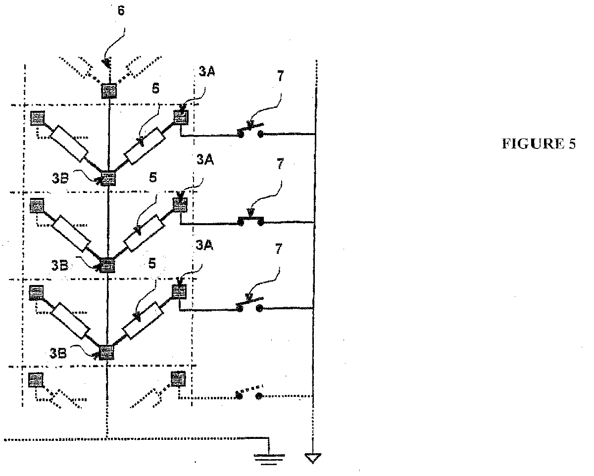
- the set of cold connections (3B) of two adjacent columns are thus connected to the same current line (6), connected as already said to a potential substantially constant.
- this cold potential line (6) is identical both columns.
- each of the bolometric detectors is connected to the reading circuit by an individual hot connection (3A), each of said connections being itself connected to a single switch (7).
- these four Microbolometer detectors share the same cold connection (3B), itself connected to the cold potential line, ie with a substantially constant potential again, we find a line of cold potential (6) identical every two columns.
- This particular provision has the advantage of further reducing additional the number of connections of the matrix.
- FIGS. 5 and 6 present a common cold connection for two or four detectors bolometric, it must be understood that any number, in particular greater than four microbolometers can share the same cold connection.
- the addressing sequence of such a microbolometer sequence is based on a traditional technique of opening and closing the switches (7) according to a sequence controlled by a clock and dedicated switches (not shown) that there is no need to detail here in more detail, because well known to those skilled in the art.
- each of the bolometric detectors is isolated from the others detectors of the same matrix, at its hot connection, who it is individual.
- the area required for to accommodate an individual connection according to the traditional techniques available is typically of the order of 6 x 6 to 8 x 8 micrometers.
- the configuration of the invention which conforms to example in Figure 6, provides a relative improvement of space of the order of 5 to 7%, an improvement in detection performance of 7 to 11%, quite advantageous in the field under consideration.
Landscapes
- Physics & Mathematics (AREA)
- General Physics & Mathematics (AREA)
- Spectroscopy & Molecular Physics (AREA)
- Photometry And Measurement Of Optical Pulse Characteristics (AREA)
Abstract
- l'une desdites structures est reliée électriquement au niveau de son autre extrémité au circuit de lecture au moyen d'une connexion électrique (3B), dite connexion froide, et portée à un potentiel sensiblement constant ;
- l'autre desdites structures est reliée électriquement au niveau de son autre extrémité au circuit de lecture également au moyen d'une connexion électrique (3A), dite connexion chaude, elle-même reliée en série avec un interrupteur (7) intégré au circuit de lecture ;
Description
- des moyens d'absorption du rayonnement infrarouge et de conversion de ce dernier en chaleur ;
- des moyens d'isolation thermique du détecteur, de telle sorte à permettre à celui-ci de s'échauffer sous l'action du rayonnement infrarouge ;
- des moyens de thermométrie, qui dans le cadre d'un détecteur bolométrique mettent en oeuvre un élément résistif ;
- et des moyens de lecture des signaux électriques fournis par les moyens de thermométrie.
- de la maítrise d'élaboration et d'intégration des matériaux bolométriques les plus performants ;
- de la maítrise des techniques de construction des détecteurs bolométriques ;
- de la qualité de mise en oeuvre des techniques pour la lecture et l'adressage de ces détecteurs et des diverses fonctions de correction qui sont utilisées dans le circuit de lecture et dans d'autres dispositifs annexes ;
- et de la maítrise des techniques de conditionnement dans un boítier étanche sous faible pression.
- l'une desdites structures est reliée électriquement au niveau de son autre extrémité au circuit de lecture au moyen d'une connexion électrique, et portée à un potentiel sensiblement constant ;
- l'autre desdites structures est reliée électriquement au niveau de son autre extrémité au circuit de lecture également au moyen d'une connexion électrique, elle-même reliée en série avec un interrupteur intégré au circuit de lecture.
Claims (3)
- Dispositif de détection infrarouge comprenant une matrice de détecteurs bolométriques connectés électriquement à un circuit de lecture (1), dans lequel chacun des détecteurs élémentaires comporte au moins deux structures d'isolation thermique conductrices électriquement (4), isolées l'une de l'autre, et montées en contact au niveau de l'une de leurs extrémités avec une zone active (5) constituée d'un matériau bolométrique, c'est à dire d'un matériau sensible, dont la résistivité varie avec la température, dans lequel :caractérisé en ce qu'au moins deux détecteurs bolométriques adjacents sont connectés par une connexion électrique commune (3B) au potentiel sensiblement constant du circuit de lecture (1).l'une desdites structures (4) est reliée électriquement au niveau de son autre extrémité au circuit de lecture (1) au moyen d'une connexion électrique (3B), dite connexion froide, et portée à un potentiel sensiblement constant ;l'autre desdites structures (4) est reliée électriquement au niveau de son autre extrémité au circuit de lecture (1) également au moyen d'une connexion électrique (3A), dite connexion chaude, elle-même reliée en série avec un interrupteur (7) intégré au circuit de lecture ;
- Dispositif de détection infrarouge selon la revendication 1, caractérisé en ce que deux détecteurs bolométriques (5) appartenant à deux colonnes adjacentes de la matrice et situés sur la même ligne sont reliés au circuit de lecture (1) par une même connexion froide (3B).
- Dispositif de détection infrarouge selon la revendication 1, caractérisé en ce que quatre détecteurs bolométriques (5) appartenant à deux colonnes adjacentes et deux lignes adjacentes de la matrice sont reliés au circuit de lecture (1) par une même connexion froide (3B).
Applications Claiming Priority (2)
| Application Number | Priority Date | Filing Date | Title |
|---|---|---|---|
| FR0313181A FR2862160B1 (fr) | 2003-11-10 | 2003-11-10 | Dispositif de detection de rayonnements infrarouges a detecteurs bolometriques |
| FR0313181 | 2003-11-10 |
Publications (2)
| Publication Number | Publication Date |
|---|---|
| EP1530238A1 true EP1530238A1 (fr) | 2005-05-11 |
| EP1530238B1 EP1530238B1 (fr) | 2008-10-15 |
Family
ID=34429967
Family Applications (1)
| Application Number | Title | Priority Date | Filing Date |
|---|---|---|---|
| EP04300759A Expired - Lifetime EP1530238B1 (fr) | 2003-11-10 | 2004-11-04 | Dispositif de détection de rayonnements infrarouges à détecteurs bolométriques |
Country Status (5)
| Country | Link |
|---|---|
| US (1) | US7148481B2 (fr) |
| EP (1) | EP1530238B1 (fr) |
| CA (1) | CA2484539A1 (fr) |
| DE (1) | DE602004017105D1 (fr) |
| FR (1) | FR2862160B1 (fr) |
Families Citing this family (5)
| Publication number | Priority date | Publication date | Assignee | Title |
|---|---|---|---|---|
| FR2918449B1 (fr) * | 2007-07-02 | 2010-05-21 | Ulis | Dispositif de detection de rayonnement infrarouge a detecteurs bolometriques |
| FR2930639B1 (fr) * | 2008-04-29 | 2011-07-01 | Ulis | Detecteur thermique a haute isolation |
| US7842533B2 (en) * | 2009-01-07 | 2010-11-30 | Robert Bosch Gmbh | Electromagnetic radiation sensor and method of manufacture |
| DE102011076046B4 (de) | 2011-05-18 | 2014-10-30 | Fraunhofer-Gesellschaft zur Förderung der angewandten Forschung e.V. | Diodensensormatrix und Verfahren zum Auslesen einer Diodensensormatrix |
| FR3100886B1 (fr) * | 2019-09-13 | 2021-12-03 | Lynred | Capteur infrarouge et procede de commande associe |
Citations (7)
| Publication number | Priority date | Publication date | Assignee | Title |
|---|---|---|---|---|
| GB2200246A (en) * | 1985-09-12 | 1988-07-27 | Plessey Co Plc | Thermal detector array |
| EP0721226A2 (fr) * | 1995-01-03 | 1996-07-10 | Texas Instruments Incorporated | Améliorations à ou concernant des éléments thermosensibles |
| US5554849A (en) * | 1995-01-17 | 1996-09-10 | Flir Systems, Inc. | Micro-bolometric infrared staring array |
| US6064066A (en) * | 1995-07-21 | 2000-05-16 | Texas Insruments Incorporated | Bolometer autocalibration |
| US6080987A (en) * | 1997-10-28 | 2000-06-27 | Raytheon Company | Infrared-sensitive conductive-polymer coating |
| US6157404A (en) * | 1995-11-15 | 2000-12-05 | Lockheed-Martin Ir Imaging Systems, Inc. | Imaging system including an array of dual-band microbridge detectors |
| US6441413B1 (en) * | 1999-11-24 | 2002-08-27 | Nec Corporation | Semiconductor device having thin film resistors made of bolometer materials |
Family Cites Families (4)
| Publication number | Priority date | Publication date | Assignee | Title |
|---|---|---|---|---|
| US6249002B1 (en) | 1996-08-30 | 2001-06-19 | Lockheed-Martin Ir Imaging Systems, Inc. | Bolometric focal plane array |
| FR2802338B1 (fr) * | 1999-12-10 | 2002-01-18 | Commissariat Energie Atomique | Dispositif de detection de rayonnement electromagnetique |
| US7034301B2 (en) * | 2002-02-27 | 2006-04-25 | Indigo Systems Corporation | Microbolometer focal plane array systems and methods |
| FR2839150B1 (fr) * | 2002-04-29 | 2004-05-28 | Commissariat Energie Atomique | Dispositif de detection thermique de rayonnement a nombre de points d'ancrage reduit |
-
2003
- 2003-11-10 FR FR0313181A patent/FR2862160B1/fr not_active Expired - Fee Related
-
2004
- 2004-11-01 CA CA002484539A patent/CA2484539A1/fr not_active Abandoned
- 2004-11-04 DE DE602004017105T patent/DE602004017105D1/de not_active Expired - Lifetime
- 2004-11-04 EP EP04300759A patent/EP1530238B1/fr not_active Expired - Lifetime
- 2004-11-05 US US10/982,335 patent/US7148481B2/en not_active Expired - Fee Related
Patent Citations (7)
| Publication number | Priority date | Publication date | Assignee | Title |
|---|---|---|---|---|
| GB2200246A (en) * | 1985-09-12 | 1988-07-27 | Plessey Co Plc | Thermal detector array |
| EP0721226A2 (fr) * | 1995-01-03 | 1996-07-10 | Texas Instruments Incorporated | Améliorations à ou concernant des éléments thermosensibles |
| US5554849A (en) * | 1995-01-17 | 1996-09-10 | Flir Systems, Inc. | Micro-bolometric infrared staring array |
| US6064066A (en) * | 1995-07-21 | 2000-05-16 | Texas Insruments Incorporated | Bolometer autocalibration |
| US6157404A (en) * | 1995-11-15 | 2000-12-05 | Lockheed-Martin Ir Imaging Systems, Inc. | Imaging system including an array of dual-band microbridge detectors |
| US6080987A (en) * | 1997-10-28 | 2000-06-27 | Raytheon Company | Infrared-sensitive conductive-polymer coating |
| US6441413B1 (en) * | 1999-11-24 | 2002-08-27 | Nec Corporation | Semiconductor device having thin film resistors made of bolometer materials |
Also Published As
| Publication number | Publication date |
|---|---|
| EP1530238B1 (fr) | 2008-10-15 |
| FR2862160A1 (fr) | 2005-05-13 |
| CA2484539A1 (fr) | 2005-05-10 |
| US7148481B2 (en) | 2006-12-12 |
| US20050098727A1 (en) | 2005-05-12 |
| FR2862160B1 (fr) | 2006-05-12 |
| DE602004017105D1 (de) | 2008-11-27 |
Similar Documents
| Publication | Publication Date | Title |
|---|---|---|
| EP0828145B1 (fr) | Détecteur infrarouge et procédé de fabrication de celui-ci | |
| EP2012101B1 (fr) | Dispositif de détection de rayonnement électromagnétique, en particulier infrarouge | |
| CA2632505C (fr) | Dispositif de detection de rayonnement infrarouge a detecteurs bolometriques | |
| CA2515104C (fr) | Dispositif de detection de rayonnements infrarouges a detecteurs bolometriques | |
| EP3384257B1 (fr) | Capteur de motif thermique | |
| FR2934044A1 (fr) | Detecteur bolometrique d'ondes electromagnetiques. | |
| EP0977275A1 (fr) | Dispositif de détection de rayonnements multispectraux infrarouge/visible | |
| FR2884608A1 (fr) | Detecteur bolometrique, dispositif de detection d'ondes electromagnetiques submillimetriques et millimetriques mettant en oeuvre un tel detecteur | |
| EP1067372A1 (fr) | Détecteur bolométrique à isolation électrique intermédiaire et procédé pour sa fabrication | |
| EP1880176B1 (fr) | Detecteur thermique de rayonnements electromagnetiques et dispositif de detection infrarouge mettant en oeuvre de tels detecteurs | |
| FR2649247A1 (fr) | Detecteur infrarouge a base de materiau pyroelectrique | |
| EP0004511A2 (fr) | Dispositif de lecture d'une cible de prise de vues et ensemble comportant un tel dispositif | |
| EP1530238B1 (fr) | Dispositif de détection de rayonnements infrarouges à détecteurs bolométriques | |
| WO2005085782A1 (fr) | Procede de realisation d’un dispositif pour la detection thermique d’un rayonnement comportant un microbolometre actif et un microbolometre passif | |
| EP0491596A1 (fr) | Détecteur infrarouge monolithique à matériau pyroélectrique | |
| FR3069938A1 (fr) | Dispositif de capture par capsules thermo-resistives adapte a un adressage passif | |
| CA2658035C (fr) | Detecteur thermique a haute isolation | |
| CA3145264A1 (fr) | Capteur infrarouge a capture instantanee | |
| EP2209305B1 (fr) | Dispositif pour la détection d'un rayonnement électromagnétique | |
| WO2018167434A1 (fr) | Capteur de rayonnement muni d'une protection anti-eblouissement | |
| FR2942074A1 (fr) | Dispositif pour la detection d'un rayonnement electromagnetique, et notamment infrarouge | |
| WO2019043312A1 (fr) | Detecteur de rayonnement electromagnetique | |
| WO2018167433A1 (fr) | Capteur de rayonnement muni d'une protection anti-eblouissement | |
| FR3055412A1 (fr) | Capteur de motifs thermiques par imagerie infrarouge d'une matrice d'elements chauffants. |
Legal Events
| Date | Code | Title | Description |
|---|---|---|---|
| PUAI | Public reference made under article 153(3) epc to a published international application that has entered the european phase |
Free format text: ORIGINAL CODE: 0009012 |
|
| AK | Designated contracting states |
Kind code of ref document: A1 Designated state(s): AT BE BG CH CY CZ DE DK EE ES FI FR GB GR HU IE IS IT LI LU MC NL PL PT RO SE SI SK TR |
|
| AX | Request for extension of the european patent |
Extension state: AL HR LT LV MK YU |
|
| 17P | Request for examination filed |
Effective date: 20050629 |
|
| AKX | Designation fees paid |
Designated state(s): DE FR GB IT SE |
|
| 17Q | First examination report despatched |
Effective date: 20071221 |
|
| GRAP | Despatch of communication of intention to grant a patent |
Free format text: ORIGINAL CODE: EPIDOSNIGR1 |
|
| GRAS | Grant fee paid |
Free format text: ORIGINAL CODE: EPIDOSNIGR3 |
|
| GRAA | (expected) grant |
Free format text: ORIGINAL CODE: 0009210 |
|
| AK | Designated contracting states |
Kind code of ref document: B1 Designated state(s): DE FR GB IT SE |
|
| REG | Reference to a national code |
Ref country code: GB Ref legal event code: FG4D Free format text: NOT ENGLISH |
|
| REF | Corresponds to: |
Ref document number: 602004017105 Country of ref document: DE Date of ref document: 20081127 Kind code of ref document: P |
|
| REG | Reference to a national code |
Ref country code: SE Ref legal event code: TRGR |
|
| PLBE | No opposition filed within time limit |
Free format text: ORIGINAL CODE: 0009261 |
|
| STAA | Information on the status of an ep patent application or granted ep patent |
Free format text: STATUS: NO OPPOSITION FILED WITHIN TIME LIMIT |
|
| 26N | No opposition filed |
Effective date: 20090716 |
|
| PGFP | Annual fee paid to national office [announced via postgrant information from national office to epo] |
Ref country code: DE Payment date: 20121113 Year of fee payment: 9 |
|
| PGFP | Annual fee paid to national office [announced via postgrant information from national office to epo] |
Ref country code: SE Payment date: 20121123 Year of fee payment: 9 Ref country code: GB Payment date: 20121127 Year of fee payment: 9 Ref country code: IT Payment date: 20121122 Year of fee payment: 9 |
|
| PGFP | Annual fee paid to national office [announced via postgrant information from national office to epo] |
Ref country code: FR Payment date: 20121220 Year of fee payment: 9 |
|
| REG | Reference to a national code |
Ref country code: SE Ref legal event code: EUG |
|
| GBPC | Gb: european patent ceased through non-payment of renewal fee |
Effective date: 20131104 |
|
| REG | Reference to a national code |
Ref country code: FR Ref legal event code: ST Effective date: 20140731 |
|
| PG25 | Lapsed in a contracting state [announced via postgrant information from national office to epo] |
Ref country code: IT Free format text: LAPSE BECAUSE OF NON-PAYMENT OF DUE FEES Effective date: 20131104 Ref country code: DE Free format text: LAPSE BECAUSE OF NON-PAYMENT OF DUE FEES Effective date: 20140603 Ref country code: SE Free format text: LAPSE BECAUSE OF NON-PAYMENT OF DUE FEES Effective date: 20131105 |
|
| REG | Reference to a national code |
Ref country code: DE Ref legal event code: R119 Ref document number: 602004017105 Country of ref document: DE Effective date: 20140603 |
|
| PG25 | Lapsed in a contracting state [announced via postgrant information from national office to epo] |
Ref country code: GB Free format text: LAPSE BECAUSE OF NON-PAYMENT OF DUE FEES Effective date: 20131104 Ref country code: FR Free format text: LAPSE BECAUSE OF NON-PAYMENT OF DUE FEES Effective date: 20131202 |