EP1528437A1 - Charging in imaging devices - Google Patents
Charging in imaging devices Download PDFInfo
- Publication number
- EP1528437A1 EP1528437A1 EP04256692A EP04256692A EP1528437A1 EP 1528437 A1 EP1528437 A1 EP 1528437A1 EP 04256692 A EP04256692 A EP 04256692A EP 04256692 A EP04256692 A EP 04256692A EP 1528437 A1 EP1528437 A1 EP 1528437A1
- Authority
- EP
- European Patent Office
- Prior art keywords
- photoconductor
- charging
- imaging
- charge
- clearance
- Prior art date
- Legal status (The legal status is an assumption and is not a legal conclusion. Google has not performed a legal analysis and makes no representation as to the accuracy of the status listed.)
- Withdrawn
Links
- 238000003384 imaging method Methods 0.000 title claims abstract description 89
- 238000000034 method Methods 0.000 claims description 15
- 239000000463 material Substances 0.000 description 17
- 238000012545 processing Methods 0.000 description 10
- 229920001971 elastomer Polymers 0.000 description 8
- 238000010586 diagram Methods 0.000 description 5
- 230000007547 defect Effects 0.000 description 4
- 239000000806 elastomer Substances 0.000 description 4
- 230000000712 assembly Effects 0.000 description 3
- 238000000429 assembly Methods 0.000 description 3
- 238000004140 cleaning Methods 0.000 description 3
- 230000002452 interceptive effect Effects 0.000 description 3
- 239000007788 liquid Substances 0.000 description 3
- 238000003860 storage Methods 0.000 description 3
- 229910052782 aluminium Inorganic materials 0.000 description 2
- XAGFODPZIPBFFR-UHFFFAOYSA-N aluminium Chemical compound [Al] XAGFODPZIPBFFR-UHFFFAOYSA-N 0.000 description 2
- 239000004020 conductor Substances 0.000 description 2
- 230000007423 decrease Effects 0.000 description 2
- 238000013461 design Methods 0.000 description 2
- 230000006870 function Effects 0.000 description 2
- 230000003993 interaction Effects 0.000 description 2
- 238000004519 manufacturing process Methods 0.000 description 2
- 239000003550 marker Substances 0.000 description 2
- 238000012546 transfer Methods 0.000 description 2
- 229920002799 BoPET Polymers 0.000 description 1
- 239000005041 Mylar™ Substances 0.000 description 1
- CBENFWSGALASAD-UHFFFAOYSA-N Ozone Chemical compound [O-][O+]=O CBENFWSGALASAD-UHFFFAOYSA-N 0.000 description 1
- 229910000831 Steel Inorganic materials 0.000 description 1
- 238000009825 accumulation Methods 0.000 description 1
- 238000007743 anodising Methods 0.000 description 1
- 238000013459 approach Methods 0.000 description 1
- 230000015556 catabolic process Effects 0.000 description 1
- 230000003247 decreasing effect Effects 0.000 description 1
- 238000011161 development Methods 0.000 description 1
- 230000000694 effects Effects 0.000 description 1
- 239000012530 fluid Substances 0.000 description 1
- 150000002500 ions Chemical class 0.000 description 1
- 229910052751 metal Inorganic materials 0.000 description 1
- 239000002184 metal Substances 0.000 description 1
- 230000003287 optical effect Effects 0.000 description 1
- 230000002093 peripheral effect Effects 0.000 description 1
- 229920000642 polymer Polymers 0.000 description 1
- 239000004065 semiconductor Substances 0.000 description 1
- 239000010959 steel Substances 0.000 description 1
Images



Classifications
-
- G—PHYSICS
- G03—PHOTOGRAPHY; CINEMATOGRAPHY; ANALOGOUS TECHNIQUES USING WAVES OTHER THAN OPTICAL WAVES; ELECTROGRAPHY; HOLOGRAPHY
- G03G—ELECTROGRAPHY; ELECTROPHOTOGRAPHY; MAGNETOGRAPHY
- G03G15/00—Apparatus for electrographic processes using a charge pattern
- G03G15/02—Apparatus for electrographic processes using a charge pattern for laying down a uniform charge, e.g. for sensitising; Corona discharge devices
- G03G15/0208—Apparatus for electrographic processes using a charge pattern for laying down a uniform charge, e.g. for sensitising; Corona discharge devices by contact, friction or induction, e.g. liquid charging apparatus
-
- G—PHYSICS
- G03—PHOTOGRAPHY; CINEMATOGRAPHY; ANALOGOUS TECHNIQUES USING WAVES OTHER THAN OPTICAL WAVES; ELECTROGRAPHY; HOLOGRAPHY
- G03G—ELECTROGRAPHY; ELECTROPHOTOGRAPHY; MAGNETOGRAPHY
- G03G15/00—Apparatus for electrographic processes using a charge pattern
- G03G15/02—Apparatus for electrographic processes using a charge pattern for laying down a uniform charge, e.g. for sensitising; Corona discharge devices
- G03G15/0208—Apparatus for electrographic processes using a charge pattern for laying down a uniform charge, e.g. for sensitising; Corona discharge devices by contact, friction or induction, e.g. liquid charging apparatus
- G03G15/025—Apparatus for electrographic processes using a charge pattern for laying down a uniform charge, e.g. for sensitising; Corona discharge devices by contact, friction or induction, e.g. liquid charging apparatus by bringing a charging member in the vicinity with the member to be charged, e.g. proximity charging, forming microgap
Definitions
- aspects of the invention relate to hard imaging apparatus charging devices, imaging assemblies, imaging assembly charging methods, and hard imaging device image bearing member charging methods.
- Charge rollers are used to charge a photoconductor in hard imaging systems (e.g., laser-printer imaging systems). Similar to Scorotron/Corona charging, charge rollers use air ionization to charge a photoconductor. However, a charge roller has increased charging efficiency (close to 100% charging efficiency) and uses lower voltages ( ⁇ 1500V) compared with Scorotron charging ( ⁇ 6500V). Physical contact of a charge roller with a photoconductor may cause print quality defects that are mainly driven by the interaction of the charge roller with materials remaining on the photoconductor after cleaning operations of the photoconductor. Materials remaining on the photoconductor may create sticky polymers which coat the photoconductor. These interactions are even more intensive with liquid electrophotographic processes where, after cleaning the photoconductor, imaging oil comprising dissolved materials and charge directors may still be present on the photoconductor surface giving rise to several print quality issues.
- a charge roller contacting a photoconductor may interact with a remaining image formed on the photoconductor, thereby creating ghosting effects (e.g., with the circumference of the charge roller). Further, the charge roller contacting the photoconductor may also interact with other materials (e.g., imaging oil) that remain on the photoconductor, contaminate the photoconductor with leak materials (e.g., conductive ions from the charge roller rubber), and create pin holes in the photoconductor in the charge roller/photoconductor nip.
- the above drawbacks may contribute to photoconductor quality issues by interfering with the photoconductor/blanket image transfer, interfering with image development, and interfering with cleaning of the photoconductor.
- the above drawbacks may also cause problems relating to photoconductor lateral conductivity, and uneven photoconductor charging. As a result, lifetime of consumables may decrease and the printing cost per page may increase.
- Other problems with liquid electrophotographic processes using a photoconductor with a seam area include print quality defects due to accumulation of imaging fluid in defects or wrap-over sections (e.g., seam regions) on the photoconductor. Movement of the charge roller over a section of the photoconductor may elevationally attract some of the accumulated materials and duplicate them into an image area.
- the extra imaging oil may not only cause disturbance of normal imaging processes but also cause disruption of the Paschen curve and the photoconductor charging voltages, thereby leading to permanent photoconductor damage.
- At least some embodiments of the invention relate to hard imaging apparatus charging devices, imaging assemblies, imaging assembly charging methods, and hard imaging device image bearing member charging methods.
- a hard imaging apparatus charging device may include first and second end members, and an intermediate member connecting the first and second end members.
- the intermediate member may have a length corresponding to an imaging area of the image bearing member.
- the intermediate member may be configured to charge the imaging area used to form latent images on the image bearing member during hard imaging operations of the hard imaging apparatus.
- the first and second end members of the charging device may be configured to maintain a predetermined spaced charging clearance between the intermediate member and the imaging area of the image bearing member.
- the first and second end members and the intermediate member of the charging device may include a monolithic layer.
- the charging device may include an outer layer configured to charge the image bearing member. The layer may be formed such that the first and second end members have a larger radius than a radius of the intermediate member.
- an imaging assembly charging method may include first providing a photoconductor having a plurality of portions of different radii, second providing a charging device configured to charge the photoconductor, rotating the photoconductor adjacent the charging device to charge the photoconductor, and third providing a clearance between the photoconductor and the charging device during charging of the photoconductor, wherein the clearance may be provided using at least one of the photoconductor or the charging device.
- the charging method may include configuring the photoconductor to have first and second end portions and an intermediate portion. The first and second end portions may be configured to have a larger radius than a radius of the intermediate portion, the radii measured from a central axis of the photoconductor.
- Fig. 1 is an exemplary diagram of a hard imaging device in accordance with one embodiment.
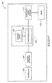
- Fig. 2 is a high-level block diagram of a hard imaging device according to one embodiment.
- Fig. 3 is a functional block diagram of a controller of the hard imaging device according to one embodiment.
- Fig. 4 is a functional schematic illustrating charging of a photoconductor using a charging device according to one embodiment.
- Figs. 5A-5C show exemplary arrangements configured to provide a clearance between a charging device and a photoconductor according to exemplary embodiments.
- Fig. 6 is a graph illustrating photoconductor to charging device clearance versus voltage in the clearance according to one embodiment.
- the hard imaging device 100 may be a laser printer. Other configurations to form hard images upon a media 212 (Fig. 2) are possible, and include for example, multifunction peripherals, copiers, facsimile devices, etc.
- Hard imaging device 100 may be embodied as a device configured to use a dry or liquid marking agent (e.g., toner) in exemplary configurations. Additional details regarding an exemplary configuration of the hard imaging device 100 are described below with respect to Fig. 2.
- the depicted hard imaging device 100 configured as a laser printer includes a controller 202, a scanning apparatus 204, an imaging assembly 205, and a developer/fusing assembly 210 configured to form hard images on media 212.
- the controller 202 may be configured to control operations of individual components (e.g., 204, 205, 210) of the hard imaging device 100.
- Exemplary operations of controller 202 include image data processing operations (e.g., rasterization) of data received from an external source (not shown), internally generated, or otherwise accessed. Further details of controller 202 are described below at Fig. 3.
- the scanning apparatus 204 may be configured to scan information formatted by controller 202 onto a photoconductor 206 to form latent images.
- Apparatus 204 may comprise a laser or other light source configured to output a light beam to scan the information in one embodiment.
- the imaging assembly 205 includes photoconductor 206 and a charging device 208 in one embodiment.
- Photoconductor 206 is alternately referred to herein as an image bearing member.
- Charging device 208 may also be referred to as a charge roller.
- Photoconductor 206 includes a rotating imaging surface (e.g., reference numeral 408 of Fig. 4) configured to receive information scanned by the scanning apparatus 204 in one embodiment.
- Imaging surface 408 is alternatively referred to herein as imaging area or imaging region.
- photoconductor 206 may be cylindrical in shape.
- An exemplary photoconductor 206 comprises a steel cylinder having outwardly exposed photoconductive material (e.g., provided in a layer). Other embodiments of image bearing member or photoconductor 206 are possible.
- photoconductor 206 may also include a non-imaging surface (e.g., reference numeral 406 of Fig. 5A).
- the non-imaging surface 406 is alternatively referred to herein as non-imaging area or non-imaging region.
- One or more lines of information may be scanned by laser scanning apparatus 204 onto imaging region 408 of photoconductor 206 forming a latent image thereon in an exemplary electrophotographic process. In the described exemplary embodiments, no information is scanned upon region 406.
- the charge roller 208 may be configured to charge photoconductor 206 to enable forming of latent images on the photoconductor 206.
- the charge roller 208 may be rotatably positioned adjacent photoconductor 206 to charge the photoconductor 206. Following charging of photoconductor 206, latent images are formed upon photoconductor 206 using scanning apparatus 204. Further details of exemplary charge rollers 208 are set forth below at Figs. 4, 5A-5C.
- the developer/fusing assembly 210 may be configured to develop information written onto the photoconductor 206 using a marking agent (e.g., toner), and transfer and fuse the developed image to media 212 (e.g., hard-imaging media such as paper, transparencies, etc.).
- a marking agent e.g., toner
- media 212 e.g., hard-imaging media such as paper, transparencies, etc.
- Fig. 3 is a detailed functional block diagram of exemplary controller 202 configured to control operations of the hard imaging device 100.
- the controller 202 includes processing circuitry 302, a storage device 304 having a database 306, and an interface 308. Other implementations of controller 202 are possible.
- Processing circuitry 302 may be configured to output data to scanning apparatus 204 and to issue command signals to photoconductor 206 and charge roller 208 to control respective operations thereof (e.g., charging of photoconductor 206 using charge roller 208, forming of latent images on the photoconductor 206, etc.).
- processing circuitry 302 may comprise circuitry configured to execute provided programming.
- processing circuitry 302 may be implemented as a microprocessor or other structure configured to execute executable instructions of programming including, for example, software and/or firmware instructions.
- Other exemplary embodiments of processing circuitry 302 include hardware logic, PGA, FPGA, ASIC, and/or other structures. These examples of processing circuitry 302 are for illustration and other configurations are possible for implementing operations discussed herein.
- the storage device 304 may be configured to store electronic data, file systems having one or more electronic files, programming such as executable instructions (e.g., software and/or firmware for use by processing circuitry 302), and/or other digital information and may include processor-usable media.
- executable instructions e.g., software and/or firmware for use by processing circuitry 302
- processor-usable media includes any article of manufacture which can contain, store, or maintain programming, data and/or digital information for use by or in connection with an instruction execution system including processing circuitry in the exemplary embodiment.
- exemplary processor-usable media may include any one of physical media such as electronic, magnetic, optical, electromagnetic, infrared or semiconductor media.
- processor-usable media include, but are not limited to, a portable magnetic computer diskette, such as a floppy diskette, zip disk, hard drive, random access memory, read only memory, flash memory, cache memory, and/or other configurations capable of storing programming, data, or other digital information.
- Interface 308 may be configured to communicate electronic data externally of the controller 202, for example, with respect to external devices of hard imaging device 100, to communicate control signals to form latent images on the photoconductor 206, etc.
- Fig. 4 is a functional schematic illustrating exemplary electrophotography aspects. For example, charging of a photoconductor 206 using a charge roller 208 in accordance with one embodiment is shown.
- photoconductor 206 may include a plurality of different regions.
- the plural regions may correspond to imaging and non-imaging regions 408, 406 (Fig. 5A), respectively, of an outer surface of photoconductor 206 having different radii or otherwise spaced different distances from a central axis 407.
- photoconductive material of photoconductor 206 may be provided in a layer 409 about a cylinder.
- imaging region 408 of the photoconductor 206 is configured to form latent images during hard imaging operations of the hard imaging device 100 (Fig. 1).
- the charge roller 208 may be positioned adjacent photoconductor 206 and configured to rotate about an axis to charge the photoconductor 206.
- the charge roller 208 may include a core member 403 (e.g., comprising a conductive material) and a layer of material 404 (e.g., high resistivity rubber) formed on the core member 403.
- the core member 403 may be configured to receive a voltage from voltage supply apparatus 410 to enable charging of the photoconductor 206.
- the charge roller 208 is positioned such that a predetermined clearance "h" is provided between the charge roller 208 and the photoconductor 206 during charging of the photoconductor 206.
- a Paschen curve describes air ionization breakdown voltages as a function of the clearance "h" between exposed electrodes.
- layer 404 of charge roller 208 and layer 409 of photoconductor 206 act as the electrodes for charging the photoconductor 206.
- a voltage Vg in the clearance "h” depends on the splitting of charge roller voltage V CR between the photoconductive material layer 409 and the clearance "h".
- V cr ( V cr - V photo - V elastomer ) ⁇ h h + L photocondictor ⁇ photocondictor
- V cr is the metal core voltage of charge roller 208
- V photo is the charge voltage of photoconductor 206
- V elastomer is the voltage drop across elastomer or rubber layer 404
- h is a clearance between exposed electrodes (e.g., a gap between electrodes comprising photoconductive material layer 409 and the charge roller 208)
- ⁇ is the dielectric constant of layer 409 of the photoconductor 206
- L is the thickness of photoconductive material layer 409 of the photoconductor 206.
- Figs. 5A-5C show respective exemplary arrangements of imaging assemblies 205, 205a, 205b to provide clearances between a photoconductor and a charge roller in order to charge the photoconductor according to various exemplary embodiments.
- Imaging assembly 205 includes a charge roller 208 having a core member 403 coated with layer 404 (e.g., high resistivity rubber or elastomer) such that end portions or members 502 of layer 404 are formed to have a larger radius R1 than a radius R2 of an intermediate portion or member 504 of layer 404, the radii being measured from a central axis 507 of the charge roller 208.
- the end portions 502 of the charge roller 208 contact and ride adjacent to regions 406 of the photoconductor 206 while maintaining a clearance "h" between the intermediate portion 504 of the charge roller 208 and region 408 of the photoconductor 206.
- intermediate portion 504 of charge roller 208 and imaging region 408 of photoconductor 206 may be of equal lengths.
- Photoconductor 206 may be made by forming a plurality of layers (not shown) on a cylindrical drum.
- Exemplary layer 409 of material coated on the cylindrical drum to form the photoconductor 206 may include Mylar, aluminum, a charge generating layer, and/or a charging transport layer.
- the plurality of regions (e.g., imaging and non-imaging regions 408, 406, respectively) of the photoconductor 206a may be made from a continuous monolithic layer of material (e.g., layer 409 (Fig. 4)), and non-imaging regions 406 may additionally be rendered electrically insulative by anodizing conductive material (e.g., aluminum) present in such regions of layer 409 of the photoconductor 206.
- end portions 502 and intermediate portion 504 of layer 404 of charge roller 208 may be formed as a continuous layer (e.g., a monolithic layer of high resistivity rubber) of material about a core member 403.
- the charge roller 208 may include a monolithic layer 404 configured to charge the photoconductor 206, and the layer 404 may be formed such that the end portions 502 have a larger radius than a radius of the intermediate portion 504.
- Photoconductor 206a may be formed as described above at Fig. 5A, but further includes a plurality of portions (e.g., end portions 506 and intermediate portion 508) made from a continuous layer (e.g., layer 409 of Fig. 4) of material formed to have different radii (e.g., R3 and R4) measured from a central axis 407a of the photoconductor 206a.
- the first and second end portions 506, also referenced as reference disks, include non-imaging regions 406a and intermediate portion 508 includes an imaging region 408a.
- non-imaging regions 406a are laterally outwardly of imaging region 408a, and non-imaging regions 406a may be rendered electrically insulative as described above at Fig. 5A.
- the charge roller 208a having a core member 403a is made as a cylindrical member having uniform radius measured from a central axis 507a of charge roller 208a.
- the first and second ends 503 of the charge roller 208a are configured to contact and ride on end portions 506 of the photoconductor 206a while a clearance "h" is maintained between region 408a of the photoconductor 206a and charge roller 208a in the depicted exemplary embodiment.
- FIG. 5C another exemplary arrangement of imaging assembly 205b to provide a different clearance "h1" between layer 404b of charge roller 208b and imaging region 408a of photoconductor 206a is shown, and wherein like elements are identified using like numerals, but with a suffix "b" added.
- Charge roller 208b of imaging assembly 205b may include a plurality of wheels 510 (e.g., wheels 510 may comprise drive members or rollers). Wheels 510 are received by core member 403b of the charge roller 208b.
- Wheels 510 have a radius R5 that is greater than the radius R6 of layer 404b and core member 403b of the charge roller 208b, the radii being measured from a central axis 507b of the charge roller 208b. Wheels 510 are configured to contact and ride adjacent to respective surfaces of end portions 506 of the photoconductor 206a, thereby providing a clearance "h1" between layer 404b of charge roller 208b and imaging region 408a of photoconductor 206a. End portions 506 of photoconductor 206a may be rendered electrically insulative as described above at Fig. 5B.
- the arrangements of charge roller 208 and photoconductor 206 may be varied to provide different design clearances "h" and "h1" between layer 404 and imaging region 408.
- Fig. 6 is an exemplary graph showing Vg as a function of the clearance "h" for three exemplary charge roller voltages (V CR ).
- the illustrated Paschen curve shows minimal voltage required for air ionization. For each V CR , ionization was observed to occur for clearances "h” as indicated in the graph, where Vg ⁇ VPaschen.
- V CR 500V for all clearances "h".
- the charging clearance corresponds to a maximum spaced distance "h" between charge roller 208 and the photoconductor 206 wherein the charging efficiency is substantially the same as if the charge roller 208 contacts the photoconductor 206.
- the charging clearance is about 19 microns with minor variations depending on such factors as the characteristics of the photoconductor layer 409, and air pressure and humidity in the charging environment, etc. Charging efficiency decreases in arrangements wherein the distance "h" exceeds this charging clearance.
- the clearance "h” is reduced for different designs of the photoconductor and charge roller, increased ionization occurs (e.g., due to lower Paschen voltage limit) thereby increasing charge on photoconductor 206 until the charging clearance is reached.
- the voltage Vg was found to be pinned to the Paschen curve until the clearance "h” reached a predetermined clearance (e.g., charging clearance).
- the charging clearance was observed to be about 19 microns in exemplary embodiments.
- the inventors have observed that if the clearance "h" drops below the charging clearance, no additional charging of the photoconductor 206 occurred as the V CR split drops Vg below the Paschen curve due to accumulated charges on the surface of the photoconductor 206.
- the charge roller 208 was observed to charge the photoconductor 206 to a maximum voltage only up to the charging clearance, and no additional charging of the photoconductor 206 occurred with clearances below the charging clearance.
- charging efficiency of the photoconductor 206 obtained at the charging clearance remained the same for all clearances "h" less than the charging clearance (e.g., from 19 microns to 0 microns), and the photoconductor 206 has been charged to its maximum potential (e.g., Charge Roller voltage -573V) at about the charging clearance.
- maximum potential e.g., Charge Roller voltage -573V
- the charging efficiency of the photoconductor 206 with clearance "h" between the charge roller 208 and the photoconductor 206 may be compared with the charging efficiency where the charge roller 208 contacts the photoconductor 206, and the results are shown in the below table: Power supply Charging efficiency Charging uniformity Ref-touching CR 1040V DC ⁇ 700 V AC, 6kHz 960V 11V PTP Non - touching CR 1040 V DC ⁇ 700V AC, 6kHz 950V 10V PTP
- Exemplary advantages of some embodiments include providing a clearance between a charge roller and a photoconductor to reduce chances of damage to the charge roller due to contact with the photoconductor. Since no direct charging of the photoconductor occurs in embodiments having a clearance between the charge roller and the photoconductor, increased charging uniformity in both in-scan and cross-scan directions may be possible. Solutions provided by some embodiments provide a charging system which is more robust to misalignments and material defects during manufacturing. Other advantages of using a spaced charge roller to charge a photoconductor include efficiencies related to cost, size, and Ozone generation rate.
Landscapes
- Physics & Mathematics (AREA)
- Engineering & Computer Science (AREA)
- Plasma & Fusion (AREA)
- General Physics & Mathematics (AREA)
- Electrostatic Charge, Transfer And Separation In Electrography (AREA)
- Discharging, Photosensitive Material Shape In Electrophotography (AREA)
Abstract
An imaging apparatus charging device (208) includes first and second end members (502),
and an intermediate member (504) connecting the first and second
end members. The intermediate member (504) may
have a length corresponding to an imaging area (408) of the image bearing
member (206) of the imaging apparatus. The intermediate member (504) may be
configured to charge the imaging area (408) used to form latent images on the image
bearing member (206) during imaging operations of the imaging apparatus.
The first and second end members (502) of the charging device (208) may be
configured to maintain a predetermined spaced charging clearance (h) between
the intermediate member (504) and the imaging area (408) of the image bearing member
(206). The first and second end members (502) and the intermediate member (504) of the
charging device (208) include a monolithic layer.
Description
- Aspects of the invention relate to hard imaging apparatus charging devices, imaging assemblies, imaging assembly charging methods, and hard imaging device image bearing member charging methods.
- Charge rollers (CRs) are used to charge a photoconductor in hard imaging systems (e.g., laser-printer imaging systems). Similar to Scorotron/Corona charging, charge rollers use air ionization to charge a photoconductor. However, a charge roller has increased charging efficiency (close to 100% charging efficiency) and uses lower voltages (∼1500V) compared with Scorotron charging (∼6500V). Physical contact of a charge roller with a photoconductor may cause print quality defects that are mainly driven by the interaction of the charge roller with materials remaining on the photoconductor after cleaning operations of the photoconductor. Materials remaining on the photoconductor may create sticky polymers which coat the photoconductor. These interactions are even more intensive with liquid electrophotographic processes where, after cleaning the photoconductor, imaging oil comprising dissolved materials and charge directors may still be present on the photoconductor surface giving rise to several print quality issues.
- In general, a charge roller contacting a photoconductor may interact with a remaining image formed on the photoconductor, thereby creating ghosting effects (e.g., with the circumference of the charge roller). Further, the charge roller contacting the photoconductor may also interact with other materials (e.g., imaging oil) that remain on the photoconductor, contaminate the photoconductor with leak materials (e.g., conductive ions from the charge roller rubber), and create pin holes in the photoconductor in the charge roller/photoconductor nip. The above drawbacks may contribute to photoconductor quality issues by interfering with the photoconductor/blanket image transfer, interfering with image development, and interfering with cleaning of the photoconductor. The above drawbacks may also cause problems relating to photoconductor lateral conductivity, and uneven photoconductor charging. As a result, lifetime of consumables may decrease and the printing cost per page may increase. Other problems with liquid electrophotographic processes using a photoconductor with a seam area include print quality defects due to accumulation of imaging fluid in defects or wrap-over sections (e.g., seam regions) on the photoconductor. Movement of the charge roller over a section of the photoconductor may elevationally attract some of the accumulated materials and duplicate them into an image area. The extra imaging oil may not only cause disturbance of normal imaging processes but also cause disruption of the Paschen curve and the photoconductor charging voltages, thereby leading to permanent photoconductor damage.
- At least some embodiments of the invention relate to hard imaging apparatus charging devices, imaging assemblies, imaging assembly charging methods, and hard imaging device image bearing member charging methods.
- In one aspect, a hard imaging apparatus charging device is disclosed. The charging device may include first and second end members, and an intermediate member connecting the first and second end members. The intermediate member may have a length corresponding to an imaging area of the image bearing member. The intermediate member may be configured to charge the imaging area used to form latent images on the image bearing member during hard imaging operations of the hard imaging apparatus. The first and second end members of the charging device may be configured to maintain a predetermined spaced charging clearance between the intermediate member and the imaging area of the image bearing member. The first and second end members and the intermediate member of the charging device may include a monolithic layer. The charging device may include an outer layer configured to charge the image bearing member. The layer may be formed such that the first and second end members have a larger radius than a radius of the intermediate member.
- In another aspect, an imaging assembly charging method is described. The charging method may include first providing a photoconductor having a plurality of portions of different radii, second providing a charging device configured to charge the photoconductor, rotating the photoconductor adjacent the charging device to charge the photoconductor, and third providing a clearance between the photoconductor and the charging device during charging of the photoconductor, wherein the clearance may be provided using at least one of the photoconductor or the charging device. The charging method may include configuring the photoconductor to have first and second end portions and an intermediate portion. The first and second end portions may be configured to have a larger radius than a radius of the intermediate portion, the radii measured from a central axis of the photoconductor.
- Other aspects of the invention are disclosed herein as is apparent from the following description and figures.
- Fig. 1 is an exemplary diagram of a hard imaging device in accordance with one embodiment.
- Fig. 2 is a high-level block diagram of a hard imaging device according to one embodiment.
- Fig. 3 is a functional block diagram of a controller of the hard imaging device according to one embodiment.
- Fig. 4 is a functional schematic illustrating charging of a photoconductor using a charging device according to one embodiment.
- Figs. 5A-5C show exemplary arrangements configured to provide a clearance between a charging device and a photoconductor according to exemplary embodiments.
- Fig. 6 is a graph illustrating photoconductor to charging device clearance versus voltage in the clearance according to one embodiment.
- Referring to Fig. 1, an exemplary hard imaging device or
apparatus 100 is shown in accordance with one embodiment of the invention. Thehard imaging device 100 may be a laser printer. Other configurations to form hard images upon a media 212 (Fig. 2) are possible, and include for example, multifunction peripherals, copiers, facsimile devices, etc.Hard imaging device 100 may be embodied as a device configured to use a dry or liquid marking agent (e.g., toner) in exemplary configurations. Additional details regarding an exemplary configuration of thehard imaging device 100 are described below with respect to Fig. 2. - Referring to Fig. 2, an exemplary high-level block diagram of the
hard imaging device 100 is shown according to one embodiment of the invention. The depictedhard imaging device 100 configured as a laser printer includes acontroller 202, ascanning apparatus 204, animaging assembly 205, and a developer/fusing assembly 210 configured to form hard images onmedia 212. - The
controller 202 may be configured to control operations of individual components (e.g., 204, 205, 210) of thehard imaging device 100. Exemplary operations ofcontroller 202 include image data processing operations (e.g., rasterization) of data received from an external source (not shown), internally generated, or otherwise accessed. Further details ofcontroller 202 are described below at Fig. 3. - The
scanning apparatus 204 may be configured to scan information formatted bycontroller 202 onto aphotoconductor 206 to form latent images.Apparatus 204 may comprise a laser or other light source configured to output a light beam to scan the information in one embodiment. - The
imaging assembly 205 includesphotoconductor 206 and acharging device 208 in one embodiment. Photoconductor 206 is alternately referred to herein as an image bearing member.Charging device 208 may also be referred to as a charge roller. -
Photoconductor 206 includes a rotating imaging surface (e.g.,reference numeral 408 of Fig. 4) configured to receive information scanned by thescanning apparatus 204 in one embodiment. Imagingsurface 408 is alternatively referred to herein as imaging area or imaging region. In one embodiment,photoconductor 206 may be cylindrical in shape. Anexemplary photoconductor 206 comprises a steel cylinder having outwardly exposed photoconductive material (e.g., provided in a layer). Other embodiments of image bearing member orphotoconductor 206 are possible. In one embodiment,photoconductor 206 may also include a non-imaging surface (e.g.,reference numeral 406 of Fig. 5A). Thenon-imaging surface 406 is alternatively referred to herein as non-imaging area or non-imaging region. One or more lines of information (e.g., information formatted by the controller 202) may be scanned bylaser scanning apparatus 204 ontoimaging region 408 ofphotoconductor 206 forming a latent image thereon in an exemplary electrophotographic process. In the described exemplary embodiments, no information is scanned uponregion 406. - The
charge roller 208 may be configured to chargephotoconductor 206 to enable forming of latent images on thephotoconductor 206. Thecharge roller 208 may be rotatably positionedadjacent photoconductor 206 to charge thephotoconductor 206. Following charging ofphotoconductor 206, latent images are formed uponphotoconductor 206 usingscanning apparatus 204. Further details ofexemplary charge rollers 208 are set forth below at Figs. 4, 5A-5C. - The developer/fusing
assembly 210 may be configured to develop information written onto thephotoconductor 206 using a marking agent (e.g., toner), and transfer and fuse the developed image to media 212 (e.g., hard-imaging media such as paper, transparencies, etc.). - Fig. 3 is a detailed functional block diagram of
exemplary controller 202 configured to control operations of thehard imaging device 100. In one embodiment, thecontroller 202 includesprocessing circuitry 302, astorage device 304 having adatabase 306, and aninterface 308. Other implementations ofcontroller 202 are possible. -
Processing circuitry 302 may be configured to output data toscanning apparatus 204 and to issue command signals tophotoconductor 206 andcharge roller 208 to control respective operations thereof (e.g., charging ofphotoconductor 206 usingcharge roller 208, forming of latent images on thephotoconductor 206, etc.). - In one embodiment,
processing circuitry 302 may comprise circuitry configured to execute provided programming. For example,processing circuitry 302 may be implemented as a microprocessor or other structure configured to execute executable instructions of programming including, for example, software and/or firmware instructions. Other exemplary embodiments ofprocessing circuitry 302 include hardware logic, PGA, FPGA, ASIC, and/or other structures. These examples ofprocessing circuitry 302 are for illustration and other configurations are possible for implementing operations discussed herein. - The
storage device 304 may be configured to store electronic data, file systems having one or more electronic files, programming such as executable instructions (e.g., software and/or firmware for use by processing circuitry 302), and/or other digital information and may include processor-usable media. For example, electronic data and/or file systems may be stored in the form of a table indatabase 306 of thestorage device 304, and stored information may be configured for retrieval by theprocessing circuitry 302. Processor-usable media includes any article of manufacture which can contain, store, or maintain programming, data and/or digital information for use by or in connection with an instruction execution system including processing circuitry in the exemplary embodiment. For example, exemplary processor-usable media may include any one of physical media such as electronic, magnetic, optical, electromagnetic, infrared or semiconductor media. Some more specific examples of processor-usable media include, but are not limited to, a portable magnetic computer diskette, such as a floppy diskette, zip disk, hard drive, random access memory, read only memory, flash memory, cache memory, and/or other configurations capable of storing programming, data, or other digital information. -
Interface 308 may be configured to communicate electronic data externally of thecontroller 202, for example, with respect to external devices ofhard imaging device 100, to communicate control signals to form latent images on thephotoconductor 206, etc. - Fig. 4 is a functional schematic illustrating exemplary electrophotography aspects. For example, charging of a
photoconductor 206 using acharge roller 208 in accordance with one embodiment is shown. - As discussed further below in accordance with some embodiments,
photoconductor 206 may include a plurality of different regions. The plural regions may correspond to imaging andnon-imaging regions 408, 406 (Fig. 5A), respectively, of an outer surface ofphotoconductor 206 having different radii or otherwise spaced different distances from acentral axis 407. In one embodiment, photoconductive material ofphotoconductor 206 may be provided in alayer 409 about a cylinder. In one embodiment,imaging region 408 of thephotoconductor 206 is configured to form latent images during hard imaging operations of the hard imaging device 100 (Fig. 1). - The
charge roller 208 may be positionedadjacent photoconductor 206 and configured to rotate about an axis to charge thephotoconductor 206. Thecharge roller 208 may include a core member 403 (e.g., comprising a conductive material) and a layer of material 404 (e.g., high resistivity rubber) formed on thecore member 403. Thecore member 403 may be configured to receive a voltage fromvoltage supply apparatus 410 to enable charging of thephotoconductor 206. In one embodiment, thecharge roller 208 is positioned such that a predetermined clearance "h" is provided between thecharge roller 208 and thephotoconductor 206 during charging of thephotoconductor 206. - A Paschen curve describes air ionization breakdown voltages as a function of the clearance "h" between exposed electrodes. In one embodiment,
layer 404 ofcharge roller 208 andlayer 409 ofphotoconductor 206 act as the electrodes for charging thephotoconductor 206. A voltage Vg in the clearance "h" depends on the splitting of charge roller voltage VCR between thephotoconductive material layer 409 and the clearance "h". The voltage Vg is provided by the following equation:charge roller 208; "Vphoto" is the charge voltage ofphotoconductor 206; "Velastomer" is the voltage drop across elastomer orrubber layer 404; "h" is a clearance between exposed electrodes (e.g., a gap between electrodes comprisingphotoconductive material layer 409 and the charge roller 208); "ε" is the dielectric constant oflayer 409 of thephotoconductor 206; and L is the thickness ofphotoconductive material layer 409 of thephotoconductor 206. - Figs. 5A-5C show respective exemplary arrangements of
imaging assemblies - Referring to Fig. 5A, an exemplary arrangement of an
imaging assembly 205 is shown.Imaging assembly 205 includes acharge roller 208 having acore member 403 coated with layer 404 (e.g., high resistivity rubber or elastomer) such that end portions ormembers 502 oflayer 404 are formed to have a larger radius R1 than a radius R2 of an intermediate portion or member 504 oflayer 404, the radii being measured from acentral axis 507 of thecharge roller 208. Theend portions 502 of thecharge roller 208 contact and ride adjacent toregions 406 of thephotoconductor 206 while maintaining a clearance "h" between the intermediate portion 504 of thecharge roller 208 andregion 408 of thephotoconductor 206. In one embodiment, intermediate portion 504 ofcharge roller 208 andimaging region 408 ofphotoconductor 206 may be of equal lengths. -
Photoconductor 206 may be made by forming a plurality of layers (not shown) on a cylindrical drum.Exemplary layer 409 of material coated on the cylindrical drum to form thephotoconductor 206 may include Mylar, aluminum, a charge generating layer, and/or a charging transport layer. The plurality of regions (e.g., imaging andnon-imaging regions non-imaging regions 406 may additionally be rendered electrically insulative by anodizing conductive material (e.g., aluminum) present in such regions oflayer 409 of thephotoconductor 206. - In one embodiment,
end portions 502 and intermediate portion 504 oflayer 404 ofcharge roller 208 may be formed as a continuous layer (e.g., a monolithic layer of high resistivity rubber) of material about acore member 403. For example, thecharge roller 208 may include amonolithic layer 404 configured to charge thephotoconductor 206, and thelayer 404 may be formed such that theend portions 502 have a larger radius than a radius of the intermediate portion 504. - Referring to Fig. 5B, another exemplary arrangement of imaging assembly 205a to provide a clearance "h" between layer 404a of
charge roller 208a and photoconductor 206a is shown, and wherein like elements are identified using like numerals, but with a suffix "a" added. Photoconductor 206a may be formed as described above at Fig. 5A, but further includes a plurality of portions (e.g., endportions 506 and intermediate portion 508) made from a continuous layer (e.g.,layer 409 of Fig. 4) of material formed to have different radii (e.g., R3 and R4) measured from a central axis 407a of the photoconductor 206a. The first andsecond end portions 506, also referenced as reference disks, includenon-imaging regions 406a andintermediate portion 508 includes animaging region 408a. In the depicted example of Fig. 5B,non-imaging regions 406a are laterally outwardly ofimaging region 408a, andnon-imaging regions 406a may be rendered electrically insulative as described above at Fig. 5A. - Continuing to refer to Fig. 5B, the
charge roller 208a having acore member 403a is made as a cylindrical member having uniform radius measured from a central axis 507a ofcharge roller 208a. The first and second ends 503 of thecharge roller 208a are configured to contact and ride onend portions 506 of the photoconductor 206a while a clearance "h" is maintained betweenregion 408a of the photoconductor 206a andcharge roller 208a in the depicted exemplary embodiment. - Referring to Fig. 5C, another exemplary arrangement of
imaging assembly 205b to provide a different clearance "h1" betweenlayer 404b of charge roller 208b andimaging region 408a of photoconductor 206a is shown, and wherein like elements are identified using like numerals, but with a suffix "b" added. Charge roller 208b ofimaging assembly 205b may include a plurality of wheels 510 (e.g.,wheels 510 may comprise drive members or rollers).Wheels 510 are received bycore member 403b of the charge roller 208b.Wheels 510 have a radius R5 that is greater than the radius R6 oflayer 404b andcore member 403b of the charge roller 208b, the radii being measured from acentral axis 507b of the charge roller 208b.Wheels 510 are configured to contact and ride adjacent to respective surfaces ofend portions 506 of the photoconductor 206a, thereby providing a clearance "h1" betweenlayer 404b of charge roller 208b andimaging region 408a of photoconductor 206a.End portions 506 of photoconductor 206a may be rendered electrically insulative as described above at Fig. 5B. - As illustrated in the exemplary embodiments of Figs. 5A-5C, the arrangements of
charge roller 208 andphotoconductor 206 may be varied to provide different design clearances "h" and "h1" betweenlayer 404 andimaging region 408. - Fig. 6 is an exemplary graph showing Vg as a function of the clearance "h" for three exemplary charge roller voltages (VCR). The illustrated Paschen curve shows minimal voltage required for air ionization. For each VCR, ionization was observed to occur for clearances "h" as indicated in the graph, where Vg ≥ VPaschen.
- As shown in the graph, the inventors have observed that no ionization occurred for VCR = 500V for all clearances "h". Minimal VCR where ionization occurred was found to be 573V with an associated clearance h=19 microns, referred to herein as the charging clearance, for exemplary photoconductors described herein. The charging clearance corresponds to a maximum spaced distance "h" between
charge roller 208 and thephotoconductor 206 wherein the charging efficiency is substantially the same as if thecharge roller 208 contacts thephotoconductor 206. Typically, the charging clearance is about 19 microns with minor variations depending on such factors as the characteristics of thephotoconductor layer 409, and air pressure and humidity in the charging environment, etc. Charging efficiency decreases in arrangements wherein the distance "h" exceeds this charging clearance. - For VCR = 700V, the inventors have observed that ionization started at a clearance "h" of 50 microns and continued until the clearance "h" was decreased to about 8 microns. Once ionization begins, the surface of the
photoconductor 206 attracts charges and counter charges, thereby increasing its surface voltage. However, surface voltage of thecharge roller 208 was not found to have significantly changed due to the attraction of counter charges ascharge roller 208 was made conductive. Hence, the voltage Vg within the clearance "h" may be reduced until the voltage reaches the Paschen value for a given clearance "h". As the clearance "h" is reduced for different designs of the photoconductor and charge roller, increased ionization occurs (e.g., due to lower Paschen voltage limit) thereby increasing charge onphotoconductor 206 until the charging clearance is reached. The voltage Vg was found to be pinned to the Paschen curve until the clearance "h" reached a predetermined clearance (e.g., charging clearance). As mentioned previously, the charging clearance was observed to be about 19 microns in exemplary embodiments. - In one exemplary case, the inventors have observed that if the clearance "h" drops below the charging clearance, no additional charging of the
photoconductor 206 occurred as the VCR split drops Vg below the Paschen curve due to accumulated charges on the surface of thephotoconductor 206. In one example, thecharge roller 208 was observed to charge thephotoconductor 206 to a maximum voltage only up to the charging clearance, and no additional charging of thephotoconductor 206 occurred with clearances below the charging clearance. For the above-noted example, charging efficiency of thephotoconductor 206 obtained at the charging clearance remained the same for all clearances "h" less than the charging clearance (e.g., from 19 microns to 0 microns), and thephotoconductor 206 has been charged to its maximum potential (e.g., Charge Roller voltage -573V) at about the charging clearance. - The charging efficiency of the
photoconductor 206 with clearance "h" between thecharge roller 208 and thephotoconductor 206 may be compared with the charging efficiency where thecharge roller 208 contacts thephotoconductor 206, and the results are shown in the below table:Power supply Charging efficiency Charging uniformity Ref-touching CR 1040V DC ±700 V AC, 6kHz 960V 11V PTP Non - touching CR 1040 V DC ±700V AC, 6kHz 950V 10V PTP - As can be seen from the above Table I, even though no contact is established between the
charge roller 208 and thephotoconductor 206 and a clearance "h" is maintained between thecharge roller 208 and thephotoconductor 206, the charging efficiency of thephotoconductor 206 remained uniform. Moreover, the charging uniformity is improved by maintaining a clearance "h" between thecharge roller 208 and thephotoconductor 206 compared to approaches wherein the charge roller contacts the photoconductor. - Exemplary advantages of some embodiments include providing a clearance between a charge roller and a photoconductor to reduce chances of damage to the charge roller due to contact with the photoconductor. Since no direct charging of the photoconductor occurs in embodiments having a clearance between the charge roller and the photoconductor, increased charging uniformity in both in-scan and cross-scan directions may be possible. Solutions provided by some embodiments provide a charging system which is more robust to misalignments and material defects during manufacturing. Other advantages of using a spaced charge roller to charge a photoconductor include efficiencies related to cost, size, and Ozone generation rate.
- The protection sought is not to be limited to the disclosed embodiments, which are given by way of example only, but instead is to be limited only by the scope of the appended claims.
Claims (10)
- A hard imaging apparatus charging device comprising:first and second end members 502; andan intermediate member 504 connecting the first and second end members and having a length corresponding to an imaging area 408 of an image bearing member 206 of a hard imaging apparatus, the intermediate member 504 configured to charge the imaging area 408 used to form latent images on the image bearing member 206 during hard imaging operations of the hard imaging apparatus, wherein the first and second end members are configured to maintain a predetermined spaced charging clearance "h" between the intermediate member 504 and the imaging area 408 of the image bearing member 206; andwherein the first and second end members and the intermediate member comprise a monolithic layer.
- The device of claim 1, wherein the charging device 208 comprises an outer layer 404 configured to charge the image bearing member, and wherein the layer is formed such that the first and second end members have a larger radius R1 than a radius of the intermediate member.
- The device of claim 1, further comprising:a member 403 for receiving a voltage from a voltage supply 410 to create ionization between the charging device 208 and the image bearing member 206 to charge the image bearing member.
- The device of claim 1, wherein the charging device is configured as a rotatable charge roller.
- The device of claim 1, wherein a radius R2 of the intermediate member is smaller than a radius R1 of the first and second end members.
- The device of claim 5, wherein the first and second end members of the charging device are configured to contact a non-imaging area 406 of the image bearing member 206 to provide the charging clearance between the intermediate member and the imaging area of the photoconductor.
- An imaging assembly charging method comprising:first providing a photoconductor 206a having a plurality of portions of different radii;second providing a charging device 208a to charge the photoconductor;rotating the photoconductor adjacent the charging device to charge the photoconductor; andthird providing a clearance "h" between the photoconductor and the charging device during charging of the photoconductor, and wherein the clearance is provided using at least one of the photoconductor or the charging device.
- The method of claim 7, wherein the first providing comprises:configuring the photoconductor to have first and second end portions 506 and an intermediate portion 508, and wherein the first and second end portions have a larger radius R3 than a radius R4 of the intermediate portion, the radii measured from a central axis 407a of the photoconductor.
- The method of claim 8, wherein the first and second end portions correspond to non-imaging areas of the photoconductor, and the intermediate portion corresponds to an imaging area of the photoconductor.
- The method of claim 7, wherein the second providing comprises:configuring the charging device 208a to have a plurality of portions 510 of different radii R5, R6; andforming the plurality of portions from a monolithic layer.
Applications Claiming Priority (2)
| Application Number | Priority Date | Filing Date | Title |
|---|---|---|---|
| US700968 | 1991-05-16 | ||
| US10/700,968 US7050742B2 (en) | 2003-10-31 | 2003-10-31 | Hard imaging apparatus charging devices and hard imaging device charging methods |
Publications (1)
| Publication Number | Publication Date |
|---|---|
| EP1528437A1 true EP1528437A1 (en) | 2005-05-04 |
Family
ID=34423472
Family Applications (1)
| Application Number | Title | Priority Date | Filing Date |
|---|---|---|---|
| EP04256692A Withdrawn EP1528437A1 (en) | 2003-10-31 | 2004-10-29 | Charging in imaging devices |
Country Status (3)
| Country | Link |
|---|---|
| US (1) | US7050742B2 (en) |
| EP (1) | EP1528437A1 (en) |
| JP (1) | JP2005141218A (en) |
Cited By (1)
| Publication number | Priority date | Publication date | Assignee | Title |
|---|---|---|---|---|
| EP3042247A4 (en) * | 2013-09-06 | 2017-04-12 | Hewlett-Packard Development Company, L.P. | Liquid electrography printing |
Families Citing this family (7)
| Publication number | Priority date | Publication date | Assignee | Title |
|---|---|---|---|---|
| JP2006350250A (en) * | 2005-06-20 | 2006-12-28 | Ricoh Co Ltd | Cleaning device and image forming apparatus using the same |
| US7756430B1 (en) | 2006-04-27 | 2010-07-13 | Hewlett-Packard Development Company, L.P. | Apparatus and method for charging an imaging member |
| US8326173B2 (en) * | 2009-09-18 | 2012-12-04 | Hewlett-Packard Development Company, L.P. | Hard imaging devices, humidity control systems and hard imaging methods |
| US8731436B2 (en) | 2011-06-01 | 2014-05-20 | Hewlett-Packard Development Company, L.P. | Positioning system for a charge roller and printer using the same |
| US9618869B2 (en) | 2012-04-30 | 2017-04-11 | Hewlett-Packard Development Company, L.P. | Printing using a metal-surface charging element |
| US9423717B2 (en) | 2012-10-15 | 2016-08-23 | Hewlett-Packard Development Company, L.P. | Charge roller for electrographic printer |
| US11143978B2 (en) | 2018-10-11 | 2021-10-12 | Hewlett-Packard Development Company, L.P. | Charge roller gap determination |
Citations (3)
| Publication number | Priority date | Publication date | Assignee | Title |
|---|---|---|---|---|
| US20030072587A1 (en) * | 2001-09-25 | 2003-04-17 | Kenji Sugiura | Charging device, image forming unit and image forming device |
| EP1331526A1 (en) * | 2000-11-02 | 2003-07-30 | Ricoh Company, Ltd. | Imaging apparatus |
| US20030190539A1 (en) * | 2001-07-26 | 2003-10-09 | Tatsuya Niimi | Electrophotographic image forming apparatus, photoreceptor therefor and method for manufacturing the photoreceptor |
Family Cites Families (16)
| Publication number | Priority date | Publication date | Assignee | Title |
|---|---|---|---|---|
| JPH03240076A (en) | 1990-02-17 | 1991-10-25 | Canon Inc | charging device |
| JPH07319326A (en) * | 1994-05-26 | 1995-12-08 | Fuji Xerox Co Ltd | Method for driving photoreceptor and flanged photoreceptor |
| KR0133524Y1 (en) * | 1996-01-29 | 1999-03-30 | 김광호 | Contact roller system for preventing pollution of exposure drum |
| US5666608A (en) | 1996-05-02 | 1997-09-09 | Hewlett-Packard Company | Charging member and image forming member spacer apparatus |
| CN1182442C (en) | 1999-10-15 | 2004-12-29 | 株式会社理光 | Photoreceptor assembly and image forming device |
| JP3844658B2 (en) | 2000-02-08 | 2006-11-15 | 株式会社リコー | Charging roller, charging device, image carrier unit, image forming apparatus, and film material winding method around charging roller |
| JP2002055512A (en) | 2000-05-30 | 2002-02-20 | Ricoh Co Ltd | Charging device and image forming apparatus having the charging device |
| JP3847583B2 (en) * | 2000-08-31 | 2006-11-22 | 株式会社リコー | Electrophotographic apparatus and process cartridge for electrophotographic apparatus |
| JP3719647B2 (en) * | 2000-09-25 | 2005-11-24 | 株式会社リコー | Charging roller, charging device, carrier unit, image forming apparatus, and manufacturing method of charging roller |
| US6795669B2 (en) * | 2001-02-02 | 2004-09-21 | Sharp Kabushiki Kaisha | Image device with control members for rollers |
| JP3795337B2 (en) * | 2001-02-23 | 2006-07-12 | 株式会社リコー | Image forming apparatus |
| JP2002278221A (en) * | 2001-03-21 | 2002-09-27 | Ricoh Co Ltd | Image forming device |
| JP2003295583A (en) * | 2002-04-05 | 2003-10-15 | Ricoh Co Ltd | Charging member / charging member surface forming method / charging device / image forming device |
| JP2004062062A (en) * | 2002-07-31 | 2004-02-26 | Ricoh Co Ltd | Charging device and image forming device |
| DE60331214D1 (en) * | 2002-09-13 | 2010-03-25 | Ricoh Kk | Charging roller with charging roller and image forming apparatus provided therewith |
| JP2004246248A (en) * | 2003-02-17 | 2004-09-02 | Ricoh Co Ltd | Image forming device |
-
2003
- 2003-10-31 US US10/700,968 patent/US7050742B2/en not_active Expired - Lifetime
-
2004
- 2004-10-29 EP EP04256692A patent/EP1528437A1/en not_active Withdrawn
- 2004-11-01 JP JP2004318030A patent/JP2005141218A/en active Pending
Patent Citations (3)
| Publication number | Priority date | Publication date | Assignee | Title |
|---|---|---|---|---|
| EP1331526A1 (en) * | 2000-11-02 | 2003-07-30 | Ricoh Company, Ltd. | Imaging apparatus |
| US20030190539A1 (en) * | 2001-07-26 | 2003-10-09 | Tatsuya Niimi | Electrophotographic image forming apparatus, photoreceptor therefor and method for manufacturing the photoreceptor |
| US20030072587A1 (en) * | 2001-09-25 | 2003-04-17 | Kenji Sugiura | Charging device, image forming unit and image forming device |
Cited By (3)
| Publication number | Priority date | Publication date | Assignee | Title |
|---|---|---|---|---|
| EP3042247A4 (en) * | 2013-09-06 | 2017-04-12 | Hewlett-Packard Development Company, L.P. | Liquid electrography printing |
| US9678454B2 (en) | 2013-09-06 | 2017-06-13 | Hewlett-Packard Development Company, L.P. | Liquid electrography printing |
| US9952527B2 (en) | 2013-09-06 | 2018-04-24 | Hewlett-Packard Development Company, L.P. | Liquid electrography printing |
Also Published As
| Publication number | Publication date |
|---|---|
| US20050095036A1 (en) | 2005-05-05 |
| US7050742B2 (en) | 2006-05-23 |
| JP2005141218A (en) | 2005-06-02 |
Similar Documents
| Publication | Publication Date | Title |
|---|---|---|
| US5146280A (en) | Charging device | |
| US7263308B2 (en) | Cleaning member, cleaning device, charging device, transfer device, process cartridge, and image forming apparatus | |
| JPH04208971A (en) | Image forming device | |
| CN106527086A (en) | Image forming apparatus | |
| US9389534B2 (en) | Image forming apparatus | |
| EP1528437A1 (en) | Charging in imaging devices | |
| US7027747B2 (en) | Method of and apparatus for forming image using a Non-Contact Charger | |
| US8849160B2 (en) | Bias charge roller having a continuous raised pattern on the outer surface | |
| US7035572B2 (en) | Hard imaging device charging systems, electrophotography charging systems, hard imaging apparatuses, and hard imaging device electrophotography charging methods | |
| US9658579B2 (en) | Image forming apparatus including a transfer bias output device | |
| JP3715350B2 (en) | Apparatus and method for storing charge on a surface | |
| US5701572A (en) | Ceramic coated detoning roll for xerographic cleaners | |
| US7242891B2 (en) | Image forming apparatus and method thereof | |
| US5815777A (en) | Image forming apparatus | |
| KR100765753B1 (en) | Developing roller and developing cartridge having same | |
| US20070025772A1 (en) | Image-Forming Device | |
| JP3862472B2 (en) | Image forming apparatus | |
| JP2003345106A (en) | Image forming apparatus | |
| US20080273898A1 (en) | Image forming apparatus | |
| JPH07333947A (en) | Charging device, image forming device, and process cartridge | |
| JPH08227204A (en) | Charging member and charging device | |
| US20050089346A1 (en) | Spaced biased roll charging member having clipped AC input voltage | |
| JP2007033497A (en) | Organic photoreceptor, process cartridge, image forming method, and image forming apparatus | |
| JPH08328439A (en) | Image forming device | |
| JP2000112255A (en) | Image forming device |
Legal Events
| Date | Code | Title | Description |
|---|---|---|---|
| PUAI | Public reference made under article 153(3) epc to a published international application that has entered the european phase |
Free format text: ORIGINAL CODE: 0009012 |
|
| AK | Designated contracting states |
Kind code of ref document: A1 Designated state(s): AT BE BG CH CY CZ DE DK EE ES FI FR GB GR HU IE IT LI LU MC NL PL PT RO SE SI SK TR |
|
| AX | Request for extension of the european patent |
Extension state: AL HR LT LV MK |
|
| AKX | Designation fees paid | ||
| REG | Reference to a national code |
Ref country code: DE Ref legal event code: 8566 |
|
| STAA | Information on the status of an ep patent application or granted ep patent |
Free format text: STATUS: THE APPLICATION IS DEEMED TO BE WITHDRAWN |
|
| 18D | Application deemed to be withdrawn |
Effective date: 20051105 |