EP1528424A1 - Optical scanner apparatuses and optical scanning methods - Google Patents
Optical scanner apparatuses and optical scanning methods Download PDFInfo
- Publication number
- EP1528424A1 EP1528424A1 EP04256528A EP04256528A EP1528424A1 EP 1528424 A1 EP1528424 A1 EP 1528424A1 EP 04256528 A EP04256528 A EP 04256528A EP 04256528 A EP04256528 A EP 04256528A EP 1528424 A1 EP1528424 A1 EP 1528424A1
- Authority
- EP
- European Patent Office
- Prior art keywords
- light beam
- scanning device
- light
- optical
- reflector
- Prior art date
- Legal status (The legal status is an assumption and is not a legal conclusion. Google has not performed a legal analysis and makes no representation as to the accuracy of the status listed.)
- Granted
Links
Images



Classifications
-
- G—PHYSICS
- G02—OPTICS
- G02B—OPTICAL ELEMENTS, SYSTEMS OR APPARATUS
- G02B27/00—Optical systems or apparatus not provided for by any of the groups G02B1/00 - G02B26/00, G02B30/00
- G02B27/0025—Optical systems or apparatus not provided for by any of the groups G02B1/00 - G02B26/00, G02B30/00 for optical correction, e.g. distorsion, aberration
- G02B27/0031—Optical systems or apparatus not provided for by any of the groups G02B1/00 - G02B26/00, G02B30/00 for optical correction, e.g. distorsion, aberration for scanning purposes
-
- G—PHYSICS
- G02—OPTICS
- G02B—OPTICAL ELEMENTS, SYSTEMS OR APPARATUS
- G02B27/00—Optical systems or apparatus not provided for by any of the groups G02B1/00 - G02B26/00, G02B30/00
- G02B27/28—Optical systems or apparatus not provided for by any of the groups G02B1/00 - G02B26/00, G02B30/00 for polarising
- G02B27/283—Optical systems or apparatus not provided for by any of the groups G02B1/00 - G02B26/00, G02B30/00 for polarising used for beam splitting or combining
Definitions
- aspects of the invention relate to optical scanner apparatuses, hard imaging devices, optical scanning methods, and hard imaging scanning methods.
- High-resolution, high-speed laser scanning exposure systems for electro-photographic printers employing rotating polygonal mirror scanners and multiple beams are known in the art.
- great care is normally required in the optical design of the scan lens to make the scan geometry at a final image plane insensitive to pyramid error (e.g., wobble) in the polygon mirror, and also to eliminate scan bow.
- Wobble may normally be prevented by bringing the multiple beams to line foci in a direction orthogonal to the scan plane at the polygon face, and then refocusing the beams at the final image plane.
- This process may require an anamorphic scan lens, which may be considerably more difficult to make, and hence more expensive, than a rotationally symmetric lens.
- This approach may also have lower performance potential due to the additional operational constraints.
- Scan bow is a variation along the length of a scan between a plurality of beams in a multi-beam scanner due to the distortion characteristics of a scan lens. If not carefully controlled, the scan lens distortion together with the compound angle effect in a rotating polygon scanner may cause scan lines lying above the middle of the scan lens' field of view to be slightly concave in an upward direction, and scan lines lying below the middle of the scan lens' field of view to be slightly concave in a downward direction.
- the scan bow may cause uppermost and lowermost scan lines to differ in shape, irrespective of placement of the swath in the field of view.
- the lowermost line from one swath and the uppermost line from the next swath form adjacent lines in the final image.
- Differences in shape between the swaths may result in visible image defects. Such defects may be made even more visible as defects repeat periodically down a page with each swath.
- Distortion of scan lens in the direction of scan is typically controlled so that a final scan coordinate is proportional to polygon scan angle ⁇ . Since ⁇ varies linearly in time due to continuous uniform rotation of the polygon, pixel information modulated onto write beam(s) at uniform time intervals may then be written at uniform spatial intervals.
- a scan lens with this distortion characteristic is commonly called an "f ⁇ " lens.
- the combination of an f ⁇ lens and a polygon scanner fails to produce straight scan lines away from the scan axis. Since in multi-beam scanning systems, all but one of the scan lines are preferred to be positioned either above or below the scan axis, such a system will exhibit scan bow.
- Anamorphic balancing takes advantage of an anamorphic lens having different distortion characteristics in the two directions normal to its optic axis. The distortion experienced by a beam traversing the lens with field components in both directions may be determined by a geometric scan of the lens' two different distortion characteristics operating separately on the beam's respective field components.
- beams scanned exactly along one axis or the other may encounter only the corresponding distortion characteristic.
- beams scanned along any other lines may encounter a composite distortion characteristic depending upon the relative magnitude of the beam's field components in the two directions. This approach allows compensation of the scan bow due to the distortion along the scan axis in a narrow region near the scan axis by a large distortion in the orthogonal direction of the opposite sign of the scan bow.
- Anamorphic balancing places additional demands upon the scan lens and restricts the degrees of freedom that may be used to satisfy other demands, such as increases in the format width and the number of resolvable spots desired of the lens.
- An alternative approach to scan bow control uses a rotationally symmetric scan lens with an fsin ⁇ distortion characteristic.
- a scan lens with this distortion exactly compensates for the scan bow characteristic of the rotating polygon mirror, resulting in zero net scan bow for scan lines placed anywhere within the field.
- the final scan coordinate may not be proportional to " ⁇ ", and information may have to be modulated onto the beam(s) at non-uniform time intervals in order to be written at uniform spatial intervals.
- Fig. 1A illustrates a plan view of a prior art arrangement 100 to overcome the inherent wobble correction defect found in a system of the fsin ⁇ type as described above.
- Wobble correction defect may be overcome by using arrangement 100 in order to permit a beam of light to double bounce off of a scanning device 102 (e.g., rotating polygon mirror).
- a scanning device 102 e.g., rotating polygon mirror
- a roof reflector 104 oriented with a roof intersection line in the plane of scan may be used to re-direct a scanned beam to the same polygon face of the scanning device 102 for a second reflection.
- the double bouncing of a beam of light has the effect of removing any change of angle in the cross-scan direction that may have been imparted to the beam due to polygon pyramid error on the first bounce from the scanning device 102.
- Fig. 1B shows an elevation view of roof reflector 104 of arrangement 100 shown in Fig. 1A.
- beam diameter at the input to an fsin ⁇ scan lens required for a scanner desired to cover a 500mm wide format with a ⁇ 30° scan to produce a ⁇ 45 micron spot diameter (FW @ 1/e 2 ) is about 15mm.
- the angle between an incoming beam to the polygon 102 and an outgoing beam to the roof reflector 104 having the minimum polygon facet length was found to be around 50°.
- An angle of 45° between an incoming beam to the polygon 102 may require the roof reflector 104 to be placed farther away from the polygon 102 to clear the lowermost scanned beam, thus requiring both a larger roof and a larger facet because of the angular spread of the scanned beams.
- a scan angle of 55° allows a slightly smaller roof to be placed closer to the polygon 102, but again requires a larger facet because of the more oblique second bounce).
- the resulting deflection system is shown in Fig. 2.
- Fig. 2 shows a double bounce deflection system 200 using a conventional roof reflector 204.
- Polygon 202 may have to be designed to have facets that are 126 mm in width. For example, for a 12-sided polygon, the facet width would correspond to a diameter of 470 mm (>18"). Such a large polygon would be relatively expensive to manufacture, and may be difficult to spin at speeds as high as 16K rpm without serious distortion of the optical figure of the facets.
- Fig. 3 shows a conventional single-bounce deflection system 300, using a polygon 302, for the same beam size and angular scan range illustrated in Fig. 2.
- the deflection system 300 may need a polygon having only six facets, individual facets having a width of only 50mm, the width corresponding to a polygon diameter of 86.6mm. This leads to increased cost and complexity, as well as limitations with respect to optical performance (i.e., such a system may not cover as wide a field at a given (high) resolution).
- the present invention seeks to provide improved optical scanning.
- optical scanner apparatus as specified in claim 1.
- At least some embodiments of the invention relate to optical scanner apparatuses, hard imaging devices, optical scanning methods, and hard imaging scanning methods.
- an optical scanner apparatus may include an optical scanning device configured to reflect a received light beam towards a photoconductor, and a beam direction system optically coupled to the optical scanning device.
- the beam direction system may include a plurality of reflectors, and each reflector may be configured to transmit light of one polarization while reflecting light of another polarization.
- the reflectors may be individually configured to permit passage of one of an input light beam provided by an external source and a light beam reflected by the scanning device and to reflect another light beam reflected by the scanning device.
- Individual ones of reflectors include polarization beam splitter coating configured to cause a light beam from the scanning device to be either reflected by the individual one of the reflectors towards another of the reflectors or transmitted through the individual one of the reflectors towards the photoconductor.
- an optical scanning method in another aspect, includes first receiving an input light beam by a scanning device, and first reflecting the input light beam towards a first reflector using the scanning device.
- the method also includes second receiving a light beam reflected by the scanning device by the first reflector, and first redirecting the light beam received by the first reflector towards a second reflector.
- the light beam received by the second reflector is redirected towards the scanning device by the second reflector, and the light beam received by the scanning device is reflected towards a photoconductor using the scanning device.
- the method preferably includes passing an input light beam through the first reflector before the first receiving, and passing the light beam output from the first reflector through a first optical device.
- the optical scanner apparatus of the present invention may be capable of covering a scan area having a relatively wide format (e.g., without a need for an anamorphic lens).
- a double bounce geometry of the optical scanner apparatus according to one embodiment may provide correction of polygon wobble, and also allow use of a smaller and more practical polygon.
- an exemplary hard imaging device 400 configured to physically render hard images upon media is shown in accordance with one embodiment.
- the hard imaging device 400 may be a laser printer.
- Other configurations to form hard images upon media are possible, and include for example, multi-function peripherals, copiers, facsimile devices, etc.
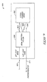
- Fig. 5 is an exemplary high-level block diagram of the hard imaging device 400 according to one embodiment.
- the depicted hard imaging device 400 configured as a laser printer includes a light source 401, a controller 402, an optical scanner apparatus 404, a photoconductor 406, a charging device 408, and a developer and fusing assembly 410 configured to form hard images on media 412.
- the light source 401 may include a laser or other light source configured to output a light beam that may be scanned by the optical scanner apparatus 404 towards photoconductor 406, in one embodiment.
- Light source 401 may emit the light beam comprising data of an image to be formed and outputted by controller 402.
- the controller 402 may be configured to control operations of one or more of individual components (e.g., 401, 404, 406, 408, and 410) of the hard imaging device 400.
- Exemplary operations of controller 402 include image data processing operations (e.g., rasterization) of data received from an external source (not shown), internally generated, or otherwise accessed.
- the optical scanner apparatus 404 may be configured to scan the beam of light (e.g., information) emitted from light source 401 onto photoconductor 406 to form latent images.
- the photoconductor 406 includes a rotating imaging surface configured to receive information scanned by the optical scanning apparatus 404.
- One or more beams of light e.g., lines of information
- the charging device 408 may be configured to charge the photoconductor 406 to enable forming of latent images on the photoconductor 406.
- charging device 408 provides a negative charge to the surface of photoconductor 406 and the scanned light beam discharges portions of the charged surface to form latent images in one embodiment.
- the developer and fusing assembly 410 may be configured to develop latent images formed on photoconductor 406 using a marking agent (e.g., toner), and transfer and fuse the developed image to media 412 (e.g., hard-imaging media such as paper, transparencies, etc.).
- a marking agent e.g., toner
- media 412 e.g., hard-imaging media such as paper, transparencies, etc.
- Fig. 6 is a plan view of an optical scanner apparatus 404 according to one embodiment.
- the optical scanner apparatus 404 includes an optical scanning device 602 (e.g., rotating polygon mirror having a plurality of facets), a beam direction system 604 (e.g., circulator), input optics 606 (e.g., a collimator system), and output optics 608 (e.g., fsin ⁇ scan lens).
- the optical scanning device 602 may be alternatively referred to as a rotating reflection device.
- a light beam from light source 401 may be received by input optics 606.
- the input optics 606 may be configured to direct the light beam from light source 401 towards beam direction system 604.
- the light beam from source 401 and input optics 606 is configured to pass through the beam direction system 604 prior to being scanned by scanning device 602 towards photoconductor 406.
- the scanned light is directed by output optics 608 to photoconductor 406 in the depicted embodiment.
- Fig. 6 depicts one fold mirror 613 configured to direct light upwardly from a horizontal direction.
- one or more additional fold mirrors may be provided to receive light from fold mirror 613 and to redirect the light from the upwardly traveling direction of Fig. 6 into a perpendicular horizontal direction towards scanning device 602.
- Other embodiments are possible for introducing light to scanning device 602.
- Fig. 7 is an exemplary block diagram of optical scanner apparatus 404 illustrating a configuration having a beam direction system 604 configured to permit passage of both an input light beam 601 from light source 401 and an output light beam 611 scanned by scanning device 602 through the beam direction system 604.
- the beam direction system 604 may be configured as an optical circulator in one embodiment.
- Beam direction system 604 is configured to permit input light beam 601 from light source 401 to pass through the beam direction system 604 to produce a light beam 603.
- the scanning device 602 reflects light beam 603 (e.g., first bounce) to produce a light beam 605 which is directed towards the beam direction system 604 for a reflection towards the scanning device 602.
- the beam direction system 604 is further configured to reflect light beam 605 received from the scanning device 602 to produce a light beam 607.
- the scanning device 602 reflects the light beam 607 (e.g., second bounce) providing and directing light beam 609 towards the beam direction system 604.
- the beam direction system 604 is configured to pass light beam 609 as light beam 611 that is scanned onto photoconductor 406. Further details of reflecting a light beam by the scanning device 602 are described below at Fig. 9A.
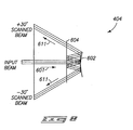
- Fig. 8 is a plan view of optical scanner apparatus 404 according to one embodiment.
- the optical scanner apparatus 404 includes a beam direction system 604 and a scanning device 602 (e.g., a plurality of facets of an exemplary device 602 comprising a polygon mirror are shown).
- the beam direction system 604 is positioned such that one or both the input and output light beams 601, 611, respectively, are permitted to pass through the beam direction system 604.
- the output light beam 611 is scanned onto photoconductor 406 by the scanning device 602.
- beam direction system 604 passing at least one of the beams 601, 611 permits the optical scanner apparatus 404 to have a smaller and more practical scanning device 602 with a compact geometry compared with the configurations of Fig. 1 A or Fig. 2, for example, while still providing relatively wide scan angles.
- Figs. 9A-9B show elevation views of an optical scanner apparatus according to various embodiments.
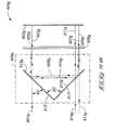
- an exemplary optical scanner apparatus 404 includes a facet of an exemplary scanning device 602 and beam direction system 604.
- the beam direction system 604 is configured and positioned such that input light beam 601, and output light beam 611 scanned by the scanning device 602 are permitted to pass through the beam direction system 604.
- a single input light beam 601 is shown for ease of illustration, a plurality of input light beams (e.g., a fan of light beams) are possible.
- beam direction system 604 includes first and second matching prisms 902a, 902b, and a third prism 904.
- the first and second matching prisms 902a, 902b may comprise reflectors such as roof reflectors and third prism 904 may comprise a roof prism in one embodiment.
- Respective surfaces 903a, 903b of the first and second prisms 902a, 902b may be coated with a polarizing beamsplitter coating 907 in order to highly transmit light of a first polarization type (e.g., horizontal polarization light components) while substantially or totally reflecting light having a polarization (e.g., vertical polarization light components) that is opposite to the first polarization type.
- a first polarization type e.g., horizontal polarization light components
- a polarization e.g., vertical polarization light components
- the first and second prisms 902a, 902b and the roof prism 904 may be attached together (e.g., using glass affixing material) to form a rectangular block 905.
- the polarization beamsplitter coating may be a multi-layer dielectric thin film polarizing beamsplitter coating.
- Other configurations of prisms 902a, 902b to permit passage of a first polarization type and reflection of a different second polarization type are possible.
- optical scanner apparatus 404 further includes optical devices 906, 908 disposed between beam direction system 604 and scanning device 602.
- optical device 908 may be a compensator, such as an O-plate.
- One exemplary O-plate is a Liquid Crystal Polymer (LCP) compensator.
- Compensator 908 may have its axis aligned at an angle of 0 degrees with respect to an entering polarization of light, and optical device 906 may be a quarter waveplate having its axis aligned at an angle of 45 degrees with respect to an entering polarization of light.
- device 906 is positioned between device 908 and scanning device 602.
- Compensator 908 may be optionally used in optical scanner apparatus 404 in order to prevent loss of desired polarization due to incomplete reflection and transmission at various device interfaces in the optical scanner apparatus 404. In other embodiments, compensator 908 is omitted, and if desired, the output power of the light source may be increased to account for losses.
- light beam 605 scanned by the scanning device 602 towards the beam direction system 604, and incoming light beam 603 received by the scanning device 602 from the beam direction system 604 are shown to trace distinct optical paths, for ease of illustration.
- the distinct optical paths result from variations (e.g., pyramid variations) present in the scanning device 602 in one example.
- an optical path of the output light beam 605 scanned by the scanning device 602 towards the beam direction system 604 retraces a path of a corresponding input light beam 603 received by the scanning device 602 from the beam direction system 604.
- the reflected light beam is then redirected towards the scanning device 602 using the first and second prisms 902a, 902b and following an optical path indicated by reference numerals 910, 911.
- the redirected light beam 911 received by the scanning device 602 is scanned towards the photoconductor 406 (Fig. 5) following optical path 914. If pyramid error is present, the light beam may be provided at a path illustrated by light beam 611.
- incoming light beam 601 encounters prism 902a and beamsplitter coating (e.g., multi-layer beamsplitter coating) provided on surface 903a of prism 902a.
- the incoming light beam 601 comprises a polarization in a same direction that the beam splitter coating on surface 903a transmits. Therefore, the incoming light beam 601 is highly transmitted and its polarization state is aligned with the polarization of the remainder of rectangular block 905 (e.g., the incoming light beam 601 passes through prism 902a and prism 904 without suffering significant losses).
- Light beam 603 output from rectangular block 905 next encounters compensator 908.
- Compensator 908 is configured to rectify any misalignments in a polarization direction of light beam 601. Compensator 908 may also be used to correct for misalignments (e.g., skew) in s- and p-planes of incidence (e.g., s-plane of incidence corresponding to a perpendicular polarization component of a light beam, and p-plane of incidence corresponding to a parallel polarization component of the light beam) when a reflected beam 605, 607 encounters prisms 902a, 902b at a compound angle of incidence (e.g., near either end of a scan) by causing a rotation in polarization of a skew light beam.
- misalignments e.g., skew
- s- and p-planes of incidence e.g., s-plane of incidence corresponding to a perpendicular polarization component of a light beam, and p-plane of incidence
- the s- and p-planes of a reflected light beam 605, 607 are rotated due to a purely geometric effect, and reflection characteristics of the multi-layer beamsplitter coating provided on surfaces 903a, 903b of respective prisms 902a, 902b are influenced by the sand p-planes of incidence of the reflected light beam.
- the compound angle of incidence may cause a portion of the reflected light beam 605, 607 desired to be reflected and transmitted at surfaces 903a, 903b to instead be transmitted and reflected and consequently lost, thereby reducing the efficiency of optical scanner apparatus 404 while also contributing to potential sources of stray light.
- compensator 908 may be used in at least some embodiments to correct the misalignments.
- Compensator 908 may also be used to produce a rotation in polarization direction of a skew light beam (e.g., light beam with misalignments in s- and p-planes of incidence) passing through it in order to compensate for the skew.
- a skew light beam e.g., light beam with misalignments in s- and p-planes of incidence
- Quarter waveplate 906 configured to convert linearly polarized light into circularly polarized light.
- linearly polarized light of entering light beam 603 is converted to a light beam having circularly polarized light by quarter waveplate 906.
- conversion may include designing a thickness of the quarter waveplate 906 such that the phase difference is 1 ⁇ 4 wavelength, and if the angle between electric field vector of an incident linearly polarized light of light beam 603 and a retarder principal plane of the quarter waveplate 906 is 45 degrees, then a light beam output from quarter waveplate 906 is circularly polarized.
- Light beam 603 with circularly polarized light and output from quarter waveplate 906 is first reflected (e.g., first bounce) by the scanning device 602 to produce light beam 605.
- handedness of the light beam 605 is reversed with respect to light beam 603 (e.g., right circular polarization is converted to left circular polarization, and vice-versa).
- the light beam 605 now encounters and passes through the quarter waveplate 906.
- polarization of the light beam 605 is converted from a circular polarization to a linear polarization that is orthogonal to a polarization state (e.g., polarization vector directed into the page in the illustrated Fig. 9A) of the incoming light beam 603.
- polarization state e.g., polarization vector directed into the page in the illustrated Fig. 9A
- Light beam 605 that is highly reflected by surface 903a of prism 902a is directed towards surface 903b of prism 902b. Since the properties of light beam 605 remain unchanged upon reflection from surface 903a, the light beam 605 is reflected by surface 903b of prism 902b towards the scanning device for a second reflection (e.g., second bounce as light beam 607).
- Light beam 607 passes through compensator 908 and quarter wave plate 906 prior to a second reflection (e.g., second bounce) by scanning device 602.
- quarter waveplate 906 Upon passing through compensator 908, quarter waveplate 906, light beam 607 and reflected light beam 609 (e.g., after second bounce from scanning device 602) encounter similar actions described above with respect to passing of light beam 601 and reflected light beam 605 (e.g., after first bounce from scanning device 602) through compensator 908, quarter waveplate 906 (e.g., conversion of linear polarization to circular polarization, and reversal of handedness upon second reflection by scanning device 602).
- the compensator 908 imparts a slight rotation to linearly polarized light beam 609 output from quarter waveplate 906 towards the photoconductor 406 (Fig. 5) in order to correct for a compound angle effect at a second encounter with prism 902b.
- light beam 609 may be strongly transmitted since its polarization is rotated to its initial direction (e.g., vertical direction in the illustrated Fig. 9A).
- Light beam 611 is then output from the beam direction system 604 for scanning onto photoconductor 406.
- a beam direction system 604a of optical scanner apparatus 404a may include a pair of flat glass plates 912a, 912b having a wire grid type polarizing coating 913.
- An exemplary wire grid type polarizing coating 913 may be obtained from Moxtek, Inc., of Orem, Utah.
- the glass plates 912a, 912b may be oriented at an angle of 90 degrees with respect to one another, and at an angle of 45 degrees with respect to an incoming light beam 601 a.
- the compensator 908 depicted in Fig. 9A is not desirable in the embodiment of Fig. 9B as the reflection characteristics of wire grid polarizing coating are not tied to the s- and p-plane directions, but are instead tied to the direction of wires used in the coating. But for the differences identified above, operation of optical scanner apparatus 404a having beam direction system 604a is substantially similar to the operation of optical scanner apparatus 404 described above at Fig. 9A.
- Exemplary advantages of the system taught herein include providing an optical scanner apparatus capable of covering a wide format (e.g., 500 mm or 700mm) due to good imaging properties of non-anamorphic scan lens, elimination of a need for an anamorphic lens to correct polygon wobble and scan bow, thereby improving performance of output optics (e.g., scan lens) to achieve a larger number of resolvable spots corresponding to a wider format, and to achieve improved resolution over a wide format compared to conventional approaches.
- Other advantages include elimination of scan bow, and correction of polygon wobble using double bounce geometry provided by the circulator while maintaining a reasonable polygon size.
- the optical scanner apparatus of the present invention may achieve a process speed of 1.5 m/sec at a print density of 813 scan lines/inch with a polygon rotation speed of 16Krpm. If a twenty four beam source is used, rotation speed of the polygon may be halved.
Landscapes
- Physics & Mathematics (AREA)
- General Physics & Mathematics (AREA)
- Optics & Photonics (AREA)
- Facsimile Scanning Arrangements (AREA)
- Mechanical Optical Scanning Systems (AREA)
- Facsimile Heads (AREA)
Abstract
Description
- Aspects of the invention relate to optical scanner apparatuses, hard imaging devices, optical scanning methods, and hard imaging scanning methods.
- High-resolution, high-speed laser scanning exposure systems for electro-photographic printers employing rotating polygonal mirror scanners and multiple beams are known in the art. In such devices, great care is normally required in the optical design of the scan lens to make the scan geometry at a final image plane insensitive to pyramid error (e.g., wobble) in the polygon mirror, and also to eliminate scan bow. Wobble may normally be prevented by bringing the multiple beams to line foci in a direction orthogonal to the scan plane at the polygon face, and then refocusing the beams at the final image plane. This process may require an anamorphic scan lens, which may be considerably more difficult to make, and hence more expensive, than a rotationally symmetric lens. This approach may also have lower performance potential due to the additional operational constraints.
- Scan bow is a variation along the length of a scan between a plurality of beams in a multi-beam scanner due to the distortion characteristics of a scan lens. If not carefully controlled, the scan lens distortion together with the compound angle effect in a rotating polygon scanner may cause scan lines lying above the middle of the scan lens' field of view to be slightly concave in an upward direction, and scan lines lying below the middle of the scan lens' field of view to be slightly concave in a downward direction.
- In multi-beam systems configured to write a plurality of scan lines at different vertical locations in a single horizontal swath, the scan bow may cause uppermost and lowermost scan lines to differ in shape, irrespective of placement of the swath in the field of view. When successive swaths are written, the lowermost line from one swath and the uppermost line from the next swath form adjacent lines in the final image. Differences in shape between the swaths may result in visible image defects. Such defects may be made even more visible as defects repeat periodically down a page with each swath.
- Distortion of scan lens in the direction of scan is typically controlled so that a final scan coordinate is proportional to polygon scan angle . Since varies linearly in time due to continuous uniform rotation of the polygon, pixel information modulated onto write beam(s) at uniform time intervals may then be written at uniform spatial intervals. A scan lens with this distortion characteristic is commonly called an "f" lens. The combination of an f lens and a polygon scanner fails to produce straight scan lines away from the scan axis. Since in multi-beam scanning systems, all but one of the scan lines are preferred to be positioned either above or below the scan axis, such a system will exhibit scan bow.
- In exemplary prior laser scanning systems, anamorphic balancing was used to provide scan bow within acceptable limits. Anamorphic balancing takes advantage of an anamorphic lens having different distortion characteristics in the two directions normal to its optic axis. The distortion experienced by a beam traversing the lens with field components in both directions may be determined by a geometric scan of the lens' two different distortion characteristics operating separately on the beam's respective field components.
- Thus, beams scanned exactly along one axis or the other may encounter only the corresponding distortion characteristic. However, beams scanned along any other lines may encounter a composite distortion characteristic depending upon the relative magnitude of the beam's field components in the two directions. This approach allows compensation of the scan bow due to the distortion along the scan axis in a narrow region near the scan axis by a large distortion in the orthogonal direction of the opposite sign of the scan bow.
- Anamorphic balancing places additional demands upon the scan lens and restricts the degrees of freedom that may be used to satisfy other demands, such as increases in the format width and the number of resolvable spots desired of the lens.
- An alternative approach to scan bow control uses a rotationally symmetric scan lens with an fsin distortion characteristic. A scan lens with this distortion exactly compensates for the scan bow characteristic of the rotating polygon mirror, resulting in zero net scan bow for scan lines placed anywhere within the field. However, in such a system, the final scan coordinate may not be proportional to "", and information may have to be modulated onto the beam(s) at non-uniform time intervals in order to be written at uniform spatial intervals.
- Fig. 1A illustrates a plan view of a
prior art arrangement 100 to overcome the inherent wobble correction defect found in a system of the fsin type as described above. Wobble correction defect may be overcome by usingarrangement 100 in order to permit a beam of light to double bounce off of a scanning device 102 (e.g., rotating polygon mirror). - Continuing to refer to Fig. 1 A, a
roof reflector 104 oriented with a roof intersection line in the plane of scan may be used to re-direct a scanned beam to the same polygon face of thescanning device 102 for a second reflection. The double bouncing of a beam of light has the effect of removing any change of angle in the cross-scan direction that may have been imparted to the beam due to polygon pyramid error on the first bounce from thescanning device 102. - Fig. 1B shows an elevation view of
roof reflector 104 ofarrangement 100 shown in Fig. 1A. Disadvantages exist with the arrangement of Fig. 1A providing the self-correction action and include utilization of a larger polygon when compared to a polygon used in a single bounce system, and particularly so if the scan angle is large. For example, beam diameter at the input to an fsin scan lens required for a scanner desired to cover a 500mm wide format with a ±30° scan to produce a ∼45 micron spot diameter (FW @ 1/e2) is about 15mm. For Fig. 1 A, the angle between an incoming beam to thepolygon 102 and an outgoing beam to theroof reflector 104 having the minimum polygon facet length was found to be around 50°. An angle of 45° between an incoming beam to thepolygon 102 may require theroof reflector 104 to be placed farther away from thepolygon 102 to clear the lowermost scanned beam, thus requiring both a larger roof and a larger facet because of the angular spread of the scanned beams. A scan angle of 55° allows a slightly smaller roof to be placed closer to thepolygon 102, but again requires a larger facet because of the more oblique second bounce). The resulting deflection system is shown in Fig. 2. - Fig. 2 shows a double
bounce deflection system 200 using aconventional roof reflector 204. Polygon 202 may have to be designed to have facets that are 126 mm in width. For example, for a 12-sided polygon, the facet width would correspond to a diameter of 470 mm (>18"). Such a large polygon would be relatively expensive to manufacture, and may be difficult to spin at speeds as high as 16K rpm without serious distortion of the optical figure of the facets. - Fig. 3 shows a conventional single-
bounce deflection system 300, using apolygon 302, for the same beam size and angular scan range illustrated in Fig. 2. Thedeflection system 300, however, may need a polygon having only six facets, individual facets having a width of only 50mm, the width corresponding to a polygon diameter of 86.6mm. This leads to increased cost and complexity, as well as limitations with respect to optical performance (i.e., such a system may not cover as wide a field at a given (high) resolution). - The present invention seeks to provide improved optical scanning.
- According to an aspect of the present invention, there is provided optical scanner apparatus as specified in
claim 1. - According to another aspect of the present invention, there is provided an optical scanning method as specified in claim 6.
- At least some embodiments of the invention relate to optical scanner apparatuses, hard imaging devices, optical scanning methods, and hard imaging scanning methods.
- In one aspect, an optical scanner apparatus is described. The optical scanner apparatus may include an optical scanning device configured to reflect a received light beam towards a photoconductor, and a beam direction system optically coupled to the optical scanning device. The beam direction system may include a plurality of reflectors, and each reflector may be configured to transmit light of one polarization while reflecting light of another polarization. The reflectors may be individually configured to permit passage of one of an input light beam provided by an external source and a light beam reflected by the scanning device and to reflect another light beam reflected by the scanning device. Individual ones of reflectors include polarization beam splitter coating configured to cause a light beam from the scanning device to be either reflected by the individual one of the reflectors towards another of the reflectors or transmitted through the individual one of the reflectors towards the photoconductor.
- In another aspect, an optical scanning method is described. The method includes first receiving an input light beam by a scanning device, and first reflecting the input light beam towards a first reflector using the scanning device. The method also includes second receiving a light beam reflected by the scanning device by the first reflector, and first redirecting the light beam received by the first reflector towards a second reflector. The light beam received by the second reflector is redirected towards the scanning device by the second reflector, and the light beam received by the scanning device is reflected towards a photoconductor using the scanning device. The method preferably includes passing an input light beam through the first reflector before the first receiving, and passing the light beam output from the first reflector through a first optical device.
- Embodiments of the present invention are described below, by way of example only, with reference to the accompanying drawings in which:
- Figs. 1A-1B show a plan view and an elevation view, respectively, of a conventional optical scanner apparatus.
- Fig. 2 shows a conventional double-bounce deflection system of an optical scanner apparatus.
- Fig. 3 shows a conventional single-bounce deflection system of an optical scanner apparatus.
- Fig. 4 is an isometric view of a hard imaging device in accordance with one embodiment.
- Fig. 5 is a high-level block diagram of a hard imaging device according to one embodiment.
- Fig. 6 is a plan view of an optical scanner apparatus according to one embodiment.
- Fig. 7 is a block diagram of an optical scanner apparatus illustrating double bouncing of a beam of light using an optical scanning device according to one embodiment.
- Fig. 8 is a plan view of an optical scanner apparatus illustrating a beam direction system according to one embodiment.
- Figs. 9A-9B show elevation views of an optical scanner apparatus illustrating a beam direction system according to various embodiments.
-
- The optical scanner apparatus of the present invention may be capable of covering a scan area having a relatively wide format (e.g., without a need for an anamorphic lens). A double bounce geometry of the optical scanner apparatus according to one embodiment may provide correction of polygon wobble, and also allow use of a smaller and more practical polygon.
- Referring to Fig. 4, an exemplary
hard imaging device 400 configured to physically render hard images upon media is shown in accordance with one embodiment. Thehard imaging device 400 may be a laser printer. Other configurations to form hard images upon media are possible, and include for example, multi-function peripherals, copiers, facsimile devices, etc. - Fig. 5 is an exemplary high-level block diagram of the
hard imaging device 400 according to one embodiment. The depictedhard imaging device 400 configured as a laser printer includes alight source 401, acontroller 402, anoptical scanner apparatus 404, aphotoconductor 406, acharging device 408, and a developer and fusingassembly 410 configured to form hard images onmedia 412. - The
light source 401 may include a laser or other light source configured to output a light beam that may be scanned by theoptical scanner apparatus 404 towardsphotoconductor 406, in one embodiment.Light source 401 may emit the light beam comprising data of an image to be formed and outputted bycontroller 402. - The
controller 402 may be configured to control operations of one or more of individual components (e.g., 401, 404, 406, 408, and 410) of thehard imaging device 400. Exemplary operations ofcontroller 402 include image data processing operations (e.g., rasterization) of data received from an external source (not shown), internally generated, or otherwise accessed. - The
optical scanner apparatus 404 may be configured to scan the beam of light (e.g., information) emitted fromlight source 401 ontophotoconductor 406 to form latent images. - The
photoconductor 406 includes a rotating imaging surface configured to receive information scanned by theoptical scanning apparatus 404. One or more beams of light (e.g., lines of information) may be scanned byoptical scanner apparatus 404 ontophotoconductor 406. - The charging
device 408 may be configured to charge thephotoconductor 406 to enable forming of latent images on thephotoconductor 406. In particular, chargingdevice 408 provides a negative charge to the surface ofphotoconductor 406 and the scanned light beam discharges portions of the charged surface to form latent images in one embodiment. - The developer and fusing
assembly 410 may be configured to develop latent images formed onphotoconductor 406 using a marking agent (e.g., toner), and transfer and fuse the developed image to media 412 (e.g., hard-imaging media such as paper, transparencies, etc.). - Fig. 6 is a plan view of an
optical scanner apparatus 404 according to one embodiment. Theoptical scanner apparatus 404 includes an optical scanning device 602 (e.g., rotating polygon mirror having a plurality of facets), a beam direction system 604 (e.g., circulator), input optics 606 (e.g., a collimator system), and output optics 608 (e.g., fsin scan lens). Theoptical scanning device 602 may be alternatively referred to as a rotating reflection device. - A light beam from light source 401 (Fig. 5) may be received by
input optics 606. Theinput optics 606 may be configured to direct the light beam fromlight source 401 towardsbeam direction system 604. In one embodiment, the light beam fromsource 401 andinput optics 606 is configured to pass through thebeam direction system 604 prior to being scanned by scanningdevice 602 towardsphotoconductor 406. The scanned light is directed byoutput optics 608 tophotoconductor 406 in the depicted embodiment. Fig. 6 depicts onefold mirror 613 configured to direct light upwardly from a horizontal direction. Although not shown in Fig. 6, one or more additional fold mirrors may be provided to receive light fromfold mirror 613 and to redirect the light from the upwardly traveling direction of Fig. 6 into a perpendicular horizontal direction towardsscanning device 602. Other embodiments are possible for introducing light toscanning device 602. - Fig. 7 is an exemplary block diagram of
optical scanner apparatus 404 illustrating a configuration having abeam direction system 604 configured to permit passage of both aninput light beam 601 fromlight source 401 and anoutput light beam 611 scanned by scanningdevice 602 through thebeam direction system 604. Thebeam direction system 604 may be configured as an optical circulator in one embodiment.Beam direction system 604 is configured to permitinput light beam 601 fromlight source 401 to pass through thebeam direction system 604 to produce alight beam 603. Thescanning device 602 reflects light beam 603 (e.g., first bounce) to produce alight beam 605 which is directed towards thebeam direction system 604 for a reflection towards thescanning device 602. Thebeam direction system 604 is further configured to reflectlight beam 605 received from thescanning device 602 to produce alight beam 607. Thescanning device 602 reflects the light beam 607 (e.g., second bounce) providing and directinglight beam 609 towards thebeam direction system 604. Thebeam direction system 604 is configured to passlight beam 609 aslight beam 611 that is scanned ontophotoconductor 406. Further details of reflecting a light beam by thescanning device 602 are described below at Fig. 9A. - Fig. 8 is a plan view of
optical scanner apparatus 404 according to one embodiment. As noted above, theoptical scanner apparatus 404 includes abeam direction system 604 and a scanning device 602 (e.g., a plurality of facets of anexemplary device 602 comprising a polygon mirror are shown). In one embodiment, thebeam direction system 604 is positioned such that one or both the input and output light beams 601, 611, respectively, are permitted to pass through thebeam direction system 604. Theoutput light beam 611 is scanned ontophotoconductor 406 by thescanning device 602. The exemplary configuration of Fig. 8 includingbeam direction system 604 passing at least one of thebeams optical scanner apparatus 404 to have a smaller and morepractical scanning device 602 with a compact geometry compared with the configurations of Fig. 1 A or Fig. 2, for example, while still providing relatively wide scan angles. - Figs. 9A-9B show elevation views of an optical scanner apparatus according to various embodiments.
- Referring to Fig. 9A, an exemplary
optical scanner apparatus 404 includes a facet of anexemplary scanning device 602 andbeam direction system 604. As noted above, thebeam direction system 604 is configured and positioned such thatinput light beam 601, andoutput light beam 611 scanned by thescanning device 602 are permitted to pass through thebeam direction system 604. Although a singleinput light beam 601 is shown for ease of illustration, a plurality of input light beams (e.g., a fan of light beams) are possible. - In one embodiment,
beam direction system 604 includes first andsecond matching prisms third prism 904. The first andsecond matching prisms third prism 904 may comprise a roof prism in one embodiment.Respective surfaces second prisms polarizing beamsplitter coating 907 in order to highly transmit light of a first polarization type (e.g., horizontal polarization light components) while substantially or totally reflecting light having a polarization (e.g., vertical polarization light components) that is opposite to the first polarization type. In one exemplary case, the first andsecond prisms roof prism 904 may be attached together (e.g., using glass affixing material) to form arectangular block 905. For the exemplary embodiment shown in Fig. 9A, the polarization beamsplitter coating may be a multi-layer dielectric thin film polarizing beamsplitter coating. Other configurations ofprisms - The
optical scanner apparatus 404 further includesoptical devices beam direction system 604 andscanning device 602. In one exemplary case,optical device 908 may be a compensator, such as an O-plate. One exemplary O-plate is a Liquid Crystal Polymer (LCP) compensator.Compensator 908 may have its axis aligned at an angle of 0 degrees with respect to an entering polarization of light, andoptical device 906 may be a quarter waveplate having its axis aligned at an angle of 45 degrees with respect to an entering polarization of light. In one embodiment,device 906 is positioned betweendevice 908 andscanning device 602.Compensator 908 may be optionally used inoptical scanner apparatus 404 in order to prevent loss of desired polarization due to incomplete reflection and transmission at various device interfaces in theoptical scanner apparatus 404. In other embodiments,compensator 908 is omitted, and if desired, the output power of the light source may be increased to account for losses. - In the embodiment of Fig. 9A,
light beam 605 scanned by thescanning device 602 towards thebeam direction system 604, and incominglight beam 603 received by thescanning device 602 from thebeam direction system 604 are shown to trace distinct optical paths, for ease of illustration. The distinct optical paths result from variations (e.g., pyramid variations) present in thescanning device 602 in one example. - However, in the absence of a pyramid error in the
scanning device 602, an optical path of theoutput light beam 605 scanned by thescanning device 602 towards thebeam direction system 604 retraces a path of a correspondinginput light beam 603 received by thescanning device 602 from thebeam direction system 604. The reflected light beam is then redirected towards thescanning device 602 using the first andsecond prisms reference numerals light beam 911 received by thescanning device 602 is scanned towards the photoconductor 406 (Fig. 5) followingoptical path 914. If pyramid error is present, the light beam may be provided at a path illustrated bylight beam 611. - In operation, with reference to exemplary
optical scanner apparatus 404 havingcompensator 908,incoming light beam 601encounters prism 902a and beamsplitter coating (e.g., multi-layer beamsplitter coating) provided onsurface 903a ofprism 902a. Theincoming light beam 601 comprises a polarization in a same direction that the beam splitter coating onsurface 903a transmits. Therefore, theincoming light beam 601 is highly transmitted and its polarization state is aligned with the polarization of the remainder of rectangular block 905 (e.g., theincoming light beam 601 passes throughprism 902a andprism 904 without suffering significant losses).Light beam 603 output fromrectangular block 905 next encounters compensator 908. -
Compensator 908 is configured to rectify any misalignments in a polarization direction oflight beam 601.Compensator 908 may also be used to correct for misalignments (e.g., skew) in s- and p-planes of incidence (e.g., s-plane of incidence corresponding to a perpendicular polarization component of a light beam, and p-plane of incidence corresponding to a parallel polarization component of the light beam) when a reflectedbeam encounters prisms - When the incidence angle is compound, the s- and p-planes of a reflected
light beam surfaces respective prisms light beam surfaces optical scanner apparatus 404 while also contributing to potential sources of stray light. Accordingly, as mentioned above,compensator 908 may be used in at least some embodiments to correct the misalignments.Compensator 908 may also be used to produce a rotation in polarization direction of a skew light beam (e.g., light beam with misalignments in s- and p-planes of incidence) passing through it in order to compensate for the skew. -
Light beam 603 after passing throughcompensator 908encounters quarter waveplate 906 configured to convert linearly polarized light into circularly polarized light. For example, linearly polarized light of enteringlight beam 603 is converted to a light beam having circularly polarized light byquarter waveplate 906. In one example, conversion may include designing a thickness of thequarter waveplate 906 such that the phase difference is ¼ wavelength, and if the angle between electric field vector of an incident linearly polarized light oflight beam 603 and a retarder principal plane of thequarter waveplate 906 is 45 degrees, then a light beam output fromquarter waveplate 906 is circularly polarized. -
Light beam 603 with circularly polarized light and output fromquarter waveplate 906 is first reflected (e.g., first bounce) by thescanning device 602 to producelight beam 605. After reflection from thescanning device 602, handedness of thelight beam 605 is reversed with respect to light beam 603 (e.g., right circular polarization is converted to left circular polarization, and vice-versa). Thelight beam 605 now encounters and passes through thequarter waveplate 906. Upon passing through thequarter waveplate 906, polarization of thelight beam 605 is converted from a circular polarization to a linear polarization that is orthogonal to a polarization state (e.g., polarization vector directed into the page in the illustrated Fig. 9A) of theincoming light beam 603. Such conversion enableslight beam 605 passing through thecompensator 908 towards therectangular block 905 to be highly reflected upon encounteringsurface 903a ofprism 902a. -
Light beam 605 that is highly reflected bysurface 903a ofprism 902a is directed towardssurface 903b ofprism 902b. Since the properties oflight beam 605 remain unchanged upon reflection fromsurface 903a, thelight beam 605 is reflected bysurface 903b ofprism 902b towards the scanning device for a second reflection (e.g., second bounce as light beam 607).Light beam 607 passes throughcompensator 908 andquarter wave plate 906 prior to a second reflection (e.g., second bounce) by scanningdevice 602. Upon passing throughcompensator 908,quarter waveplate 906,light beam 607 and reflected light beam 609 (e.g., after second bounce from scanning device 602) encounter similar actions described above with respect to passing oflight beam 601 and reflected light beam 605 (e.g., after first bounce from scanning device 602) throughcompensator 908, quarter waveplate 906 (e.g., conversion of linear polarization to circular polarization, and reversal of handedness upon second reflection by scanning device 602). Thecompensator 908 imparts a slight rotation to linearly polarizedlight beam 609 output fromquarter waveplate 906 towards the photoconductor 406 (Fig. 5) in order to correct for a compound angle effect at a second encounter withprism 902b. Upon encounteringprism 902b,light beam 609 may be strongly transmitted since its polarization is rotated to its initial direction (e.g., vertical direction in the illustrated Fig. 9A).Light beam 611 is then output from thebeam direction system 604 for scanning ontophotoconductor 406. - Referring to Fig. 9B, another exemplary embodiment of optical scanner apparatus is shown wherein like elements are identified with like numerals with a suffix "a" added. In this embodiment, instead of
prisms optical scanner apparatus 404a may include a pair offlat glass plates 912a, 912b having a wire gridtype polarizing coating 913. An exemplary wire gridtype polarizing coating 913 may be obtained from Moxtek, Inc., of Orem, Utah. In one exemplary case, theglass plates 912a, 912b may be oriented at an angle of 90 degrees with respect to one another, and at an angle of 45 degrees with respect to an incoming light beam 601 a. Thecompensator 908 depicted in Fig. 9A is not desirable in the embodiment of Fig. 9B as the reflection characteristics of wire grid polarizing coating are not tied to the s- and p-plane directions, but are instead tied to the direction of wires used in the coating. But for the differences identified above, operation ofoptical scanner apparatus 404a having beam direction system 604a is substantially similar to the operation ofoptical scanner apparatus 404 described above at Fig. 9A. - Exemplary advantages of the system taught herein include providing an optical scanner apparatus capable of covering a wide format (e.g., 500 mm or 700mm) due to good imaging properties of non-anamorphic scan lens, elimination of a need for an anamorphic lens to correct polygon wobble and scan bow, thereby improving performance of output optics (e.g., scan lens) to achieve a larger number of resolvable spots corresponding to a wider format, and to achieve improved resolution over a wide format compared to conventional approaches. Other advantages include elimination of scan bow, and correction of polygon wobble using double bounce geometry provided by the circulator while maintaining a reasonable polygon size. For example, using a twelve beam laser array source and twelve facet polygon, the optical scanner apparatus of the present invention may achieve a process speed of 1.5 m/sec at a print density of 813 scan lines/inch with a polygon rotation speed of 16Krpm. If a twenty four beam source is used, rotation speed of the polygon may be halved.
- The protection sought is not to be limited to the disclosed embodiments, which are given by way of example only, but instead is to be limited only by the scope of the appended claims.
- The disclosures in United States patent application No. 10/700,957, from which this application claims priority, and in the abstract accompanying this application are incorporated herein by reference.
Claims (10)
- Optical scanner apparatus (404) including:an optical scanning device (602) configured to reflect a received light beam towards a photoconductor (406);a beam direction system (604) optically coupled to the optical scanning device and including plurality of reflectors (902a, 902b), each reflector configured to transmit light of one polarization while reflecting light of another polarization; andwherein the reflectors are individually configured to permit passage of one of an input light beam provided by an external source and a light beam reflected by the scanning device and to reflect another light beam reflected by the scanning device.
- Apparatus as in claim 1, wherein individual ones of reflectors (902a, 902b) include a polarization beam splitter coating (907) configured to cause a light beam from the scanning device (602) to be either reflected by the individual one of the reflectors towards another of the reflectors or transmitted through the individual one of the reflectors towards the photoconductor.
- Apparatus of claim 1, wherein individual ones of the reflectors (092a, 902b) include a beam splitter coating configured to pass light of a first polarization direction and reflect light having a polarization direction opposition to the first polarization direction.
- Apparatus as in claim 1, 2 or 3, including:a first optical device (906) disposed between the beam direction system and the optical scanning device and configured to convert a first type of polarized light into a second type of polarized light to cause a light beam reflected by the scanning device to be reflected upon encountering a first reflector among the plurality of reflectors.
- Apparatus as in claim 4, including:a second optical device (908) disposed between the beam direction system and the first optical device to reduce stray light components from passing therethrough.
- An optical scanning method, including the steps of:first receiving an input light beam by a scanning device (602);first reflecting the input light beam towards a first reflector (902a) using the scanning device;second receiving a light beam reflected by the scanning device by the first reflector;first redirecting the light beam received by the first reflector towards a second reflector (902b);second redirecting the light beam received by the second reflector towards the scanning device (602) to increase a scan angle of the light beam; andsecond reflecting the light beam redirected by the second reflector onto a photoconductor (406) using the scanning device.
- A method as in claim 6, including:passing the input light beam through the first reflector (902a) before the first receiving; andpassing the light beam output from the firs reflector through a first optical device (906).
- A method as in claim 7, including converting light of a first polarization type to light of a second polarization type using the first optical device (906).
- A method as in claim 8, including:arranging the first optical device (906) comprising a quarter waveplate at an angle of substantially 45 degrees with respect to an incoming polarization direction in order to reflect a light beam reflected by the scanning device towards the second reflector (902b).
- A method as in claim 9, including:arranging a second optical device (908) including a compensator at an angle of substantially 0 degrees with respect to an incoming polarization direction to rectify misalignment of a light beam passing through the second optical device.
Applications Claiming Priority (2)
| Application Number | Priority Date | Filing Date | Title |
|---|---|---|---|
| US10/700,957 US7142340B2 (en) | 2003-10-31 | 2003-10-31 | Optical scanner apparatuses and optical scanning methods |
| US700957 | 2003-10-31 |
Publications (2)
| Publication Number | Publication Date |
|---|---|
| EP1528424A1 true EP1528424A1 (en) | 2005-05-04 |
| EP1528424B1 EP1528424B1 (en) | 2007-12-19 |
Family
ID=34423470
Family Applications (1)
| Application Number | Title | Priority Date | Filing Date |
|---|---|---|---|
| EP04256528A Expired - Lifetime EP1528424B1 (en) | 2003-10-31 | 2004-10-22 | Optical scanner apparatuses and optical scanning methods |
Country Status (4)
| Country | Link |
|---|---|
| US (1) | US7142340B2 (en) |
| EP (1) | EP1528424B1 (en) |
| JP (1) | JP4203000B2 (en) |
| DE (1) | DE602004010769T2 (en) |
Cited By (2)
| Publication number | Priority date | Publication date | Assignee | Title |
|---|---|---|---|---|
| US8228581B2 (en) | 2008-09-26 | 2012-07-24 | Prsym, Inc. | Scanning optical device |
| US10279426B2 (en) | 2015-08-14 | 2019-05-07 | Laser Engineering Applications | Machining device |
Families Citing this family (3)
| Publication number | Priority date | Publication date | Assignee | Title |
|---|---|---|---|---|
| KR100601647B1 (en) * | 2003-12-05 | 2006-07-14 | 삼성전자주식회사 | Gwangju Yarn Equipment |
| JP6342842B2 (en) | 2015-04-30 | 2018-06-13 | オリンパス株式会社 | Scanning microscope system |
| TWI815252B (en) * | 2021-12-22 | 2023-09-11 | 財團法人工業技術研究院 | Light emission module, light detection and ranging system and light scanning method |
Citations (5)
| Publication number | Priority date | Publication date | Assignee | Title |
|---|---|---|---|---|
| JPS60205419A (en) * | 1984-03-30 | 1985-10-17 | Fuji Photo Film Co Ltd | Light beam scanner |
| US4796965A (en) * | 1984-06-22 | 1989-01-10 | Fuji Photo Film Co., Ltd. | Optical scanning device |
| EP0423812A2 (en) * | 1989-10-20 | 1991-04-24 | Canon Kabushiki Kaisha | Scanning optical apparatus |
| WO2003009048A1 (en) * | 2001-07-20 | 2003-01-30 | The University Of Reading | Scanning apparatus |
| US6587246B1 (en) * | 1998-09-02 | 2003-07-01 | Qinetiq Limited | Scanning apparatus |
Family Cites Families (6)
| Publication number | Priority date | Publication date | Assignee | Title |
|---|---|---|---|---|
| DE2843282A1 (en) * | 1977-10-05 | 1979-04-12 | Canon Kk | PHOTOELECTRIC DETECTION DEVICE |
| US4662709A (en) * | 1984-07-23 | 1987-05-05 | Xerox Corporation | Wobble correction by two reflectors on an internally reflecting facet without bow |
| US5576854A (en) * | 1993-11-12 | 1996-11-19 | Hughes-Jvc Technology Corporation | Liquid crystal light valve projector with improved contrast ratio and with 0.27 wavelength compensation for birefringence in the liquid crystal light valve |
| US5475524A (en) * | 1994-12-19 | 1995-12-12 | Xerox Corporation | Optics for passive facet tracking and passive scan angle doubling |
| US5491578A (en) * | 1994-12-19 | 1996-02-13 | Xerox Corporation | Optics for passive scan angle doubling |
| US6061080A (en) * | 1998-01-30 | 2000-05-09 | Xerox Corporation | Aperture for multiple reflection raster output scanning system to reduce bow |
-
2003
- 2003-10-31 US US10/700,957 patent/US7142340B2/en not_active Expired - Fee Related
-
2004
- 2004-10-22 DE DE602004010769T patent/DE602004010769T2/en not_active Expired - Lifetime
- 2004-10-22 EP EP04256528A patent/EP1528424B1/en not_active Expired - Lifetime
- 2004-11-01 JP JP2004318029A patent/JP4203000B2/en not_active Expired - Fee Related
Patent Citations (5)
| Publication number | Priority date | Publication date | Assignee | Title |
|---|---|---|---|---|
| JPS60205419A (en) * | 1984-03-30 | 1985-10-17 | Fuji Photo Film Co Ltd | Light beam scanner |
| US4796965A (en) * | 1984-06-22 | 1989-01-10 | Fuji Photo Film Co., Ltd. | Optical scanning device |
| EP0423812A2 (en) * | 1989-10-20 | 1991-04-24 | Canon Kabushiki Kaisha | Scanning optical apparatus |
| US6587246B1 (en) * | 1998-09-02 | 2003-07-01 | Qinetiq Limited | Scanning apparatus |
| WO2003009048A1 (en) * | 2001-07-20 | 2003-01-30 | The University Of Reading | Scanning apparatus |
Non-Patent Citations (1)
| Title |
|---|
| PATENT ABSTRACTS OF JAPAN vol. 010, no. 064 (P - 436) 14 March 1986 (1986-03-14) * |
Cited By (2)
| Publication number | Priority date | Publication date | Assignee | Title |
|---|---|---|---|---|
| US8228581B2 (en) | 2008-09-26 | 2012-07-24 | Prsym, Inc. | Scanning optical device |
| US10279426B2 (en) | 2015-08-14 | 2019-05-07 | Laser Engineering Applications | Machining device |
Also Published As
| Publication number | Publication date |
|---|---|
| JP4203000B2 (en) | 2008-12-24 |
| JP2005141217A (en) | 2005-06-02 |
| US7142340B2 (en) | 2006-11-28 |
| US20050094231A1 (en) | 2005-05-05 |
| DE602004010769T2 (en) | 2008-12-24 |
| DE602004010769D1 (en) | 2008-01-31 |
| EP1528424B1 (en) | 2007-12-19 |
Similar Documents
| Publication | Publication Date | Title |
|---|---|---|
| US7956884B2 (en) | Optical scanning device and image forming apparatus | |
| US5526166A (en) | Optical system for the correction of differential scanline bow | |
| EP0727686B1 (en) | Optical scanner having curved mirrors for F-theta and curved field compensation | |
| US7705872B2 (en) | Optical writing device and image forming apparatus | |
| EP0604077A2 (en) | Multiple beam diode laser output scanning system | |
| US6930812B2 (en) | Multi-beam light scanning optical system and image forming apparatus using same | |
| US5550668A (en) | Multispot polygon ROS with maximized line separation depth of focus | |
| US8922863B2 (en) | Optical scanning device and image forming apparatus | |
| US8373736B2 (en) | Optical scanning device and image forming apparatus | |
| US7142340B2 (en) | Optical scanner apparatuses and optical scanning methods | |
| US6963433B2 (en) | Multibeam scanning optical device and image forming apparatus using the same | |
| EP0710009B1 (en) | Method and apparatus reducing differences in images heights of images generated by plural light beams having dissimilar wavelengths | |
| JP2013200441A (en) | Optical scanner and image forming apparatus | |
| US6222663B1 (en) | High duty cycle scanner for laser printer | |
| US7557820B2 (en) | Optical multi-beam scanning device and image forming apparatus | |
| JP5251571B2 (en) | Optical scanning device and image forming apparatus | |
| JP2002350763A (en) | Laser scanner and image forming device provided with the same | |
| JP2004184527A (en) | Optical scanning device and image forming apparatus | |
| JP2009092943A (en) | Optical scanning device and image forming device | |
| JP2012103523A (en) | Optical scanner and image forming apparatus | |
| JPH04361218A (en) | Optical scanning device | |
| JP2004163739A (en) | Optical device and scanning optical device having the same | |
| JPH0467007A (en) | scanning optical device | |
| JP2002214553A (en) | Optical scanning device and image forming apparatus |
Legal Events
| Date | Code | Title | Description |
|---|---|---|---|
| PUAI | Public reference made under article 153(3) epc to a published international application that has entered the european phase |
Free format text: ORIGINAL CODE: 0009012 |
|
| AK | Designated contracting states |
Kind code of ref document: A1 Designated state(s): AT BE BG CH CY CZ DE DK EE ES FI FR GB GR HU IE IT LI LU MC NL PL PT RO SE SI SK TR |
|
| AX | Request for extension of the european patent |
Extension state: AL HR LT LV MK |
|
| 17P | Request for examination filed |
Effective date: 20051103 |
|
| AKX | Designation fees paid |
Designated state(s): DE FR GB |
|
| GRAP | Despatch of communication of intention to grant a patent |
Free format text: ORIGINAL CODE: EPIDOSNIGR1 |
|
| GRAS | Grant fee paid |
Free format text: ORIGINAL CODE: EPIDOSNIGR3 |
|
| GRAA | (expected) grant |
Free format text: ORIGINAL CODE: 0009210 |
|
| AK | Designated contracting states |
Kind code of ref document: B1 Designated state(s): DE FR GB |
|
| REG | Reference to a national code |
Ref country code: GB Ref legal event code: FG4D |
|
| REF | Corresponds to: |
Ref document number: 602004010769 Country of ref document: DE Date of ref document: 20080131 Kind code of ref document: P |
|
| ET | Fr: translation filed | ||
| PLBE | No opposition filed within time limit |
Free format text: ORIGINAL CODE: 0009261 |
|
| STAA | Information on the status of an ep patent application or granted ep patent |
Free format text: STATUS: NO OPPOSITION FILED WITHIN TIME LIMIT |
|
| 26N | No opposition filed |
Effective date: 20080922 |
|
| PGFP | Annual fee paid to national office [announced via postgrant information from national office to epo] |
Ref country code: FR Payment date: 20121107 Year of fee payment: 9 |
|
| PGFP | Annual fee paid to national office [announced via postgrant information from national office to epo] |
Ref country code: GB Payment date: 20130923 Year of fee payment: 10 |
|
| PGFP | Annual fee paid to national office [announced via postgrant information from national office to epo] |
Ref country code: DE Payment date: 20130920 Year of fee payment: 10 |
|
| REG | Reference to a national code |
Ref country code: FR Ref legal event code: ST Effective date: 20140630 |
|
| PG25 | Lapsed in a contracting state [announced via postgrant information from national office to epo] |
Ref country code: FR Free format text: LAPSE BECAUSE OF NON-PAYMENT OF DUE FEES Effective date: 20131031 |
|
| REG | Reference to a national code |
Ref country code: DE Ref legal event code: R119 Ref document number: 602004010769 Country of ref document: DE |
|
| GBPC | Gb: european patent ceased through non-payment of renewal fee |
Effective date: 20141022 |
|
| PG25 | Lapsed in a contracting state [announced via postgrant information from national office to epo] |
Ref country code: DE Free format text: LAPSE BECAUSE OF NON-PAYMENT OF DUE FEES Effective date: 20150501 Ref country code: GB Free format text: LAPSE BECAUSE OF NON-PAYMENT OF DUE FEES Effective date: 20141022 |