EP1528039A1 - Method for manufacturing a single electron device by electro-migration of nanoclusters and corresponding single electron device - Google Patents
Method for manufacturing a single electron device by electro-migration of nanoclusters and corresponding single electron device Download PDFInfo
- Publication number
- EP1528039A1 EP1528039A1 EP04025635A EP04025635A EP1528039A1 EP 1528039 A1 EP1528039 A1 EP 1528039A1 EP 04025635 A EP04025635 A EP 04025635A EP 04025635 A EP04025635 A EP 04025635A EP 1528039 A1 EP1528039 A1 EP 1528039A1
- Authority
- EP
- European Patent Office
- Prior art keywords
- nanoclusters
- metallic
- passivated
- single electron
- metal
- Prior art date
- Legal status (The legal status is an assumption and is not a legal conclusion. Google has not performed a legal analysis and makes no representation as to the accuracy of the status listed.)
- Withdrawn
Links
Images




Classifications
-
- B—PERFORMING OPERATIONS; TRANSPORTING
- B82—NANOTECHNOLOGY
- B82B—NANOSTRUCTURES FORMED BY MANIPULATION OF INDIVIDUAL ATOMS, MOLECULES, OR LIMITED COLLECTIONS OF ATOMS OR MOLECULES AS DISCRETE UNITS; MANUFACTURE OR TREATMENT THEREOF
- B82B3/00—Manufacture or treatment of nanostructures by manipulation of individual atoms or molecules, or limited collections of atoms or molecules as discrete units
-
- B—PERFORMING OPERATIONS; TRANSPORTING
- B82—NANOTECHNOLOGY
- B82Y—SPECIFIC USES OR APPLICATIONS OF NANOSTRUCTURES; MEASUREMENT OR ANALYSIS OF NANOSTRUCTURES; MANUFACTURE OR TREATMENT OF NANOSTRUCTURES
- B82Y10/00—Nanotechnology for information processing, storage or transmission, e.g. quantum computing or single electron logic
-
- B—PERFORMING OPERATIONS; TRANSPORTING
- B82—NANOTECHNOLOGY
- B82Y—SPECIFIC USES OR APPLICATIONS OF NANOSTRUCTURES; MEASUREMENT OR ANALYSIS OF NANOSTRUCTURES; MANUFACTURE OR TREATMENT OF NANOSTRUCTURES
- B82Y30/00—Nanotechnology for materials or surface science, e.g. nanocomposites
-
- B—PERFORMING OPERATIONS; TRANSPORTING
- B82—NANOTECHNOLOGY
- B82Y—SPECIFIC USES OR APPLICATIONS OF NANOSTRUCTURES; MEASUREMENT OR ANALYSIS OF NANOSTRUCTURES; MANUFACTURE OR TREATMENT OF NANOSTRUCTURES
- B82Y40/00—Manufacture or treatment of nanostructures
-
- H—ELECTRICITY
- H10—SEMICONDUCTOR DEVICES; ELECTRIC SOLID-STATE DEVICES NOT OTHERWISE PROVIDED FOR
- H10D—INORGANIC ELECTRIC SEMICONDUCTOR DEVICES
- H10D30/00—Field-effect transistors [FET]
- H10D30/01—Manufacture or treatment
- H10D30/014—Manufacture or treatment of FETs having zero-dimensional [0D] or one-dimensional [1D] channels, e.g. quantum wire FETs, single-electron transistors [SET] or Coulomb blockade transistors
-
- H—ELECTRICITY
- H10—SEMICONDUCTOR DEVICES; ELECTRIC SOLID-STATE DEVICES NOT OTHERWISE PROVIDED FOR
- H10N—ELECTRIC SOLID-STATE DEVICES NOT OTHERWISE PROVIDED FOR
- H10N99/00—Subject matter not provided for in other groups of this subclass
- H10N99/05—Devices based on quantum mechanical effects, e.g. quantum interference devices or metal single-electron transistors
-
- Y—GENERAL TAGGING OF NEW TECHNOLOGICAL DEVELOPMENTS; GENERAL TAGGING OF CROSS-SECTIONAL TECHNOLOGIES SPANNING OVER SEVERAL SECTIONS OF THE IPC; TECHNICAL SUBJECTS COVERED BY FORMER USPC CROSS-REFERENCE ART COLLECTIONS [XRACs] AND DIGESTS
- Y10—TECHNICAL SUBJECTS COVERED BY FORMER USPC
- Y10S—TECHNICAL SUBJECTS COVERED BY FORMER USPC CROSS-REFERENCE ART COLLECTIONS [XRACs] AND DIGESTS
- Y10S438/00—Semiconductor device manufacturing: process
- Y10S438/969—Simultaneous formation of monocrystalline and polycrystalline regions
Definitions
- the present invention relates to a method for manufacturing a single electron device by electro-migration of nanoclusters.
- the invention also relates to a single electron device comprising a quantum dot as single electron component housed on a patterned substrate which includes at least an electrode.
- the enclosed Figure 1 illustrates the basic concept of single-electronics.
- the island does not generate any appreciable electric field beyond its borders, and a even weak external force F may bring in an additional electron from outside.
- this injection is carried out by a tunneling effect through an energy barrier created by a thin insulating layer. Now, after this injection, the net charge Q of the island would be (- e ), and the resulting electric field E would repulse any further electron that might be added.
- the electric field E that it generates is inversely proportional to the square of the island size, and may become rather strong for nanoscale structures.
- the electric field is as large as ⁇ 140 kV/cm on the surface of a 10-nm sphere in vacuum.
- E a E c + E k ( 2 )
- Figure 2 shows the total electron addition energy as a function of the island diameter, as calculated using Eq. (2) for a simple but representative model.
- E a is dominated by the charging energy E c and is of the order of 1 meV, i.e. ⁇ 10 K in temperature units.
- a single-electron addition energy Ea is shown as a solid line, while the charging energy Ec is shown as dashed line and the electron kinetic energy E k as dotted line, all calculated using Eqs. (1) and (2) for a simple model of a conducting island.
- dielectric constant e 4
- the simplest device that shows single electron phenomena is the "single-electron box” like that shown in Figure 3a, and reported by K.K. Likharev.
- This device comprises just one small island separated from a larger electrode ("electron source”) by a tunnel barrier.
- An external electric field may be applied to the island using another electrode (“ gate ”) separated from the island by a thicker insulator, which does not allow noticeable tunneling.
- the field changes the electrochemical potential of the island and thus determines the conditions of electron tunneling.
- This device allows to verify experimentally the phenomenon, known as "Coulomb staircase", which is gradually smeared out by thermal fluctuations if the temperature is increased to k B T ⁇ E c .
- Coulomb staircase is a very simple physic phenomenon: increasing gate voltage U attracts more and more electrons to the island. The discreteness of electron transfer through low transparency barriers necessarily makes this increase step-like. Then even such a simple device allows a reliable addition/subtraction of single electrons to/from an island with an enormous (and unknown) number of background electrons, of the order of 1 million in typical low-temperature experiments with 100-nm-scale aluminum islands.
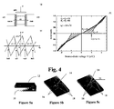
- Figures 4a to 4c relates to capacitive-coupled single-electron transistor, and in particular show: (a) schema, (b) source-drain dc I-V curves of a symmetric transistor for several values of the Qe, i.e. of the gate voltage, and (c) the Coulomb blockade threshold voltage V t as a function of Q e at T ⁇ 0.
- FIG. 4b shows typical dc I - V curves of this system.
- V t At small source-drain voltage V t there is no current, since any tunneling event would lead to an increase of the total energy ( ⁇ W ⁇ 0) and hence at low enough temperatures ( k B T ⁇ E c ) the tunneling rate is exponentially low.
- This suppression of dc current at low voltages is known as the Coulomb blockade.
- V t the Coulomb blockade is overcome, and at much higher voltages the dc I - V curve gradually approaches one of the offset linear asymptotes: I ⁇ ( V + sign ( V ) ⁇ ( e / 2C ⁇ ))/ (R 1 + R 2 )
- the I-V curve exhibits quasi-periodic oscillations of its slope, closely related in nature to the Coulomb staircase in the single-electron box, and expressed especially strongly in the case of a strong difference between R 1 and R 2 .
- the fabrication methods can be divided as physical or chemical techniques according to the main procedures.
- the physical methods often utilize the combination of thin film and lithographic technologies.
- the aim of the present invention is that of providing a new and original solution for the manufacturing of single electron device, preferably, but not necessarily, working at room temperatures.
- the solution idea behind the present invention is that of developing single electron (SE) devices working preferably, but not necessarily, at room temperature using a new technology process and building up a set of nanocontacts that can be self-assembled and able to maintain a desired separation distance, particularly in the ⁇ 10 nm range, including as well a quantum dot made up of a single nanoparticle, which can be sized in the same range.
- SE single electron
- a patterned substrate over which nanoclusters are forced to assembly under the control of a not homogeneous electric field is employed.
- the substrate may be patterned by a lithographic technique or by other techniques such as SAM (Self Assembled Monolayers); MicroPrinting or DNA-Scaffolding.
- the substrate could be a polimeric substrate; glass or ITO; that is: a non silicon substrate.
- the present invention realizes a single-electron or SE device working at room temperature by employing a lithographic patterned substrate over which nanoclusters are forced to assembly under the control of a not homogeneous electric field.
- the controlled migration and the desired location of the metallic passivated nanoclusters are based on the a dielectrophoretic process, which is well-known by itself but has never been applied in this field.
- the method comprises, as a first phase, the realization of a patterned substrate.
- a central aperture 14 and paths 16 for metallic contacts and peripheral apertures 18 are opened, leaving a thickness of the oxide layer 12 over the Si substrate 10.
- the central aperture 14 is rectangular and has a depth of about three times its width.
- the pads 22 have free-contact surfaces, four in this example, are available as electrodes for the dielectrophoresis control.
- the method comprises, as a second phase, the deposition of nanoclusters by means of a dielectrophoresis process.
- the deposition phase exploits metallic nanoclusters as building blocks to growth up nanowires, under the control of an external electric field.
- the first method has a great disadvantage due to the fact that metal reacts chemically with carbon tube walls and the research of remedies is in running.
- the method comprises the steps of:
- the inventive process comprises a deposition phase which in turn includes the following steps:
- the step of synthesis of metallic nanoclusters in turn comprises the steps of:
- a polyol process is used to prepare finely divided powders of easily reducible metals.
- a suitable solid inorganic compound in particular a starting metal compound, is suspended in liquid polyol.
- the suspension is stirred and heated to a given temperature that can reach the boiling point of the polyol for the less easily reducible metals.
- the reduction of the starting metal compound quantitatively yields the metal as a finely divided powder.
- This starting compound may be a hydroxide, an oxide, and a convenient salt.
- the reduction to metal can be achieved employing various polyols, ethylene glycol (EG), and diethylene glycol (DEG) being the mainly used.
- the reduction reaction proceeds in polyvinylpyrrolidone (PVP, Aldrich M w 10000) that acts as reducing agent and inhibitor of the aggregation process of the nanoclusters so formed.
- the main feature of this reaction mechanism is that the reduction reaction proceeds via the solution rather than in the solid state. Therefore, the metal particles are formed by nucleation and growth from the solution. This main feature is quite general for all investigated reactions and for all metals obtained by this polyol process.
- the polyol acts first as a solvent for the starting inorganic or metal compound.
- the occurrence in the above described reaction of an intermediate solid phase between the starting material and the final metal powder is not quite general but is very frequently observed.
- the metal Me is generated in the liquid phase and when the supersaturation of such solution is high enough, nucleation and growth occur.
- the metal particles or metallic nanoclusters so formed are isotropic; the homogeneous nucleation model explaining these characteristics with an effective separation between the nucleation and growth steps.
- the grow parameters of the above described chemical synthesis of active metal allow to control the size of metallic cores while, as will be explained hereunder, the kind of thiol, and in particular the number n of the groups (CH 2 ) defines the thickness of the shell and therefore the size of the conductive barrier and the linear resolution of the process.
- the reaction temperature influences the morphological characteristics of the metal particles. As a general rule a decrease of the mean size of the metal particles is observed as the reaction temperature increase.
- the metallic nanoclusters are stabilized by superficial treatment via thiol.
- the metallic suspension obtained after the nucleation and growth of the metal particles is cooled and treated at room temperature with a dodecanthiol (CH 3 (CH 2 ) 11 SH) solution or with a thiol excess having the following formula: CH 3 (CH 2 ) n SH, where n is an integer.
- a dodecanthiol (CH 3 (CH 2 ) 11 SH) solution or with a thiol excess having the following formula: CH 3 (CH 2 ) n SH, where n is an integer.
- a concentrated solution is prepared by adding PVP to the metallic suspension and, then, thiol molecules are chemically absorbed to the nanoclusters surface following the reaction: Me n + m R-SH ⁇ Me n (SR) m + m/2 H 2
- the metallic nanoclusters are separated by extraction with hydrocarbon (wet-way process) or by addition of water followed by filtration (dry-way process). Hexane is mainly used as hydrocarbon for wet-way process.
- the metallic nanoclusters are purified by dissolution in ethyl alcohol and precipitation with acetone.
- the precipitation product is separated by centrifugation and made dry to the air.
- the method of the invention then follows with a phase of nanoclusters deposition by dielectrophoresis.
- dielectrophoresis As it is well kwon, the process of dielectrophoresis (DEP) is defined as the motion of neutral, polarizable matter produced by a non-uniform electric (AC or DC) field, see for instance the work of H. A. Pohl, "Dielectrophoresis", Cambridge University Press, Cambridge, 1978.
- dielectrophoresis process is fully distinguished from the electrophoresis process, which is the motion of charged particles in a uniform electric field.
- the principle of DEP lies in the fact that a net force can arise upon even neutral particles situated in a non-uniform electric field.
- a force acts on the particle.
- This force can be thought as rising from a two step process comprising a first step of induction or alignment of an electric dipole included in the particles followed by a second step of application of unequal forces of the end of that dipole. Since the two equally charged ends of the dipole lie in unequal field strengths of the diverging field, a net force arises.
- the DEP-induced particle motion is strongly dependent on the field frequency, the spatial configuration of the electrodes responsible of field generation, the dielectric properties of the suspended medium and of the particle itself.
- the dipole aligns against the field and particle is repelled from the regions of high electric field. So the force is unaffected by the direction of the electric field, responding only to the field gradient. Since the alignment of the field is irrelevant one could generate the electric field in AC, with the advantage of reducing any electrophoretic force, due to any net particle charge, to zero.
- magnitude of F DEP depends on the frequency of the AC electric field, since real and imaginary part of f CM are very different according to the work frequency (as can be shown in Figure 8). It's useful to set the working frequency so as to choose the weight of each of the two contributes of the force, linked to the real or the imaginary part.
- the real component of f CM is usually used to trap the particle, while the imaginary component is for translational particle actuation.
- the field induced force increases as field gradient becomes stronger.
- An increase of field gradient can be obtained by miniaturization of the electrodes.
- FIG. 9 A schematic view of a polarizable particle suspended within a point-plane electrode system is shown in Figure 9.
- the system 30 includes a plane electrode 32 and a point electrode 34 with a particle 36 between the electrodes.
- the particle 36 polarizes, the interaction between the dipolar charges with the local electric field produces a force.
- the force is greater in the side facing the point electrode 34 than that on the side facing the plane electrode 32, and there is net motion of the particle 36 towards the point electrode 34.
- This effect is called positive dielectrophoresis. If the particle 36 is less polarizable than the surrounding medium, the dipole of the particle 36 will align in opposition with respect to the electric field and the particle 36 will be repelled from the high field regions. This effect is called negative dielectrophoresis.
- the method according to the invention further comprises a phase of realization of a nanocontact.
- nanocontact realization phase comprises in turn:
- the thioles degradation may be performed even by UV treatment.
- the process may even not require a treatment for thioles degradation since in case of very thin thioles barriers (about nm) the tunneling effect could assure a significant conduction.
- the so-created nanocontact 56 is the new reference point for the others nanoclusters 52 since the force lines of the electric field get denser close to a smaller radius curvature region such as the nanocontact itself, as shown in figures 11 A and 11 B.
- metallic nanoclusters could be deposited for catalytic applications, in such a way to realize catalytic material by a dielectric deposition.
- a possible application for these kind of metallic nanoclusters is the growing of nano-tubes or the use as catalytic loads in polimeric electrodes.
- the method for producing a SE device comprises a first step of patterning of a substrate, as already described above with reference to figures 5A-5C.
- a flat electrode 60 is suspended parallel to the patterned substrate without contacting it, as can be seen in Figure 12. Also shown in figure 13 is an enlarged view of a central aperture 14 of the patterned substrate, wherein North, East, South and West electrodes (respectively indicated as 62, 64, 66 and 68) formed in the paths 16 are highlighted.
- the central aperture 14 is rectangular and the electrodes 62, 64, 66, 68 are substantially central located with respect to the central aperture sides.
- the distance between the electrode 60 and the patterned substrate is one of the design parameters which allows to control the curvature of the force lines of the electric field and so the dielectrophoresis force as well as the potential applied to it.
- a potential difference is applied between the four electrodes 62, 64, 66 and 68, held to the same potential and the plate-electrode 60: the configuration of the electrodes 62, 64, 66 and 68 is chosen so as to let the absolute root value of the electric field have its maximum next to the free face of the four electrodes 62, 64, 66 and 68 facing the central aperture 14.
- nanowires 70 are generated and represent a powerful matter to link the nanometric world of the quantum dot to the macroscopic easily managed world of the patterned electrodes.
- the metallic passivated nanoclusters 52 are forced to assembly under control of a non homogeneous electric field, said process step being performed at room temperature.
- the ability to control precisely the process of self-assembly nanoclusters is depending on the uniformity of the electric field between the top electrode 60, acting as flat panel, and the four electrodes 62, 64, 66 and 68 where the nanoclusters are self-assembled.
- an integrated microcavity is realized in order to guarantee the possibility to act a fine control of the distance d z between the top electrode 60 and the patterned substrate as well as the control of its shape, and so in order to precisely control the nanowire assembly.
- the process of Figures 14-18 begins similarly to the process of Figures 5A-5C with the formation of a thin silicon oxide layer (SiO 2 ) 12 on a silicon (Si) substrate 10 as shown in Figure 14. Then, instead of etching a central aperture 14 and contact pads 16 in the silicon oxide layer 12, as in Figures 5A-5C, advantageously according to the invention, the process comprises a step of depositing aluminum or other metal contacts 72 on the silicon oxide layer 12, in such a way to form a central aperture 74 (which correspond to the central aperture 14 of Figure 13) between the metal contacts 72, as shown in Figure 15.
- the process further comprises a step of forming a silicon nitride sacrifical layer 76 in such a way to fill the central aperture 74 and to cover at least portions of the metal contact 72, as shown in Figure 16.
- the thin silicon oxide layer 12 is then grown to form a thick silicon oxide layer 78 laterally of the silicon nitride sacrifical layer 76 and on the metal contacts 72, as shown in Figure 17.
- the process still further comprises a step of removing the silicon nitride sacrifical layer 76 so forming the integrated microcavity 82.
- the process comprises a step of forming a plate electrode 60 on the thick silicon oxide layer 78 and above the central aperture 74, so closing the microcavity 82, as shown in Figure 18.
- the process comprises a phase of forming nanowires 70 within the integrated microcavity 82 according to the dielectrophoretic process described above with reference of Figures 12 and 13, so obtaining a complete single electron (SE) structure 80.
- SE single electron
- the central aperture 14 in the patterned substrate is chosen rectangular in order to have, for example, a distance between the N-S electrodes 62, 66 bigger than distance between the E-W electrodes, 64, 68.
- the WE electrodes distance is chosen of the order of 10nm.
- a typical size for the central aperture 14 of the microcavity is 90x150nm 2 (that can be obtained for instance by conventional lithography techniques) and 30nm for electrodes width so that, if the nanowires 70 are developed with a final length of about 40nm, it will results in a W-E electrodes distance of about 10nm and a N-S electrodes distance of about 70nm.
- the gap between the so obtained nanowires 70 starting from the electrodes 62, 64, 66, 68 defines a location for a metallic passivated nanocluster acting as quantum dot.
- the maximum value of the electric field absolute root applied by the plate electrode 60 lets a nanocluster occupy such a nanowires gap, so obtaining a complete SE structure 80, as shown in figure 18.
- This structure 80 including four terminal electrodes (62, 64, 66, 68) may be used, for example, as an AND/OR logic gate.
- the process can easy be extended to integrate more than one Single Electron (SE) Devices in a single microcavity as well as to integrate both SE devices with conventional components and circuits (for example to integrate the signal amplifiers and conditioning circuits, as well as to develop a buried resistor grid which will act as the heater for the thioles degradation in the final steps of the nanowires realization).
- SE Single Electron
- the invention also relates to a single electron device comprising a quantum dot as single electron component housed on a patterned substrate 10 or 40 which includes at least an electrode connected by at least a nanowire 70 to the quantum dot.
- the single electron device shown in the figures as a preferred embodiment of the present invention, comprises a plurality of electrodes 62, 64, 66, 68 connected by a plurality of nanowires 70 to the quantum dot, the gap between the nanowires 70 defining a location for the quantum dot, as explained above.
- the quantum dot is realized by a metallic passivated nanocluster 52, according to the present invention.
- the single electron device according to the present invention includes a microcavity 82 having a central aperture 14, 74 surrounded by the electrodes 62, 64, 66, 68 and housing the nanowires 70 as well as the quantum dot.
- quantum dot involves the use of treated carbon structures (C 60 based molecules) or Si clusters surrounded by a SiO 2 dielectric shell.
- the method of the present invention does solve the technical problem and achieves various advantages and benefits.
- SE-box basic single-electron devices
- SE-transistor SE Turnstile and pump
- SE transistor oscillators analog application
- analog application supersensitive electrometry, SE spectroscopy, CD current standards, temperature standards, resistance standards, detection of infrared radiation
- digital application voltage state logics, charge state logics, SET/FET memory, NOVAROM
- the proposed structure can be used either as a SET device, driving both the gate electrodes with the same control signal, or as a logic gate, driving each gate electrode with a suitable digital signal.
- the latter can be used either as an OR or as an AND gate, depending on the signal value applied at each gate electrode.
Landscapes
- Engineering & Computer Science (AREA)
- Chemical & Material Sciences (AREA)
- Nanotechnology (AREA)
- Crystallography & Structural Chemistry (AREA)
- Physics & Mathematics (AREA)
- General Physics & Mathematics (AREA)
- Manufacturing & Machinery (AREA)
- Condensed Matter Physics & Semiconductors (AREA)
- Composite Materials (AREA)
- Materials Engineering (AREA)
- Mathematical Physics (AREA)
- Theoretical Computer Science (AREA)
- Thin Film Transistor (AREA)
Abstract
The present invention relates to a method for manufacturing a single electron device (80)
by electro-migration of nanoclusters (52). The inventive method comprises the steps of:
- patterning a substrate (10, 40);
- preparing metallic passivated nanoclusters (52);
- forcing the metallic passivated nanoclusters (52) to assembly over the patterned substrate (10) under control of a non homogeneous electric field.
The invention also relates to a single electron device comprising a quantum dot as single
electron component.
Description
- The present invention relates to a method for manufacturing a single electron device by electro-migration of nanoclusters.
- The invention also relates to a single electron device comprising a quantum dot as single electron component housed on a patterned substrate which includes at least an electrode.
- To fully understand all the aspects of the present invention reference is made to the enclosed Figures 1-4 showing known examples of single-electron devices.
- The enclosed Figure 1 illustrates the basic concept of single-electronics.
- Let's first consider a small electroneutral conductor, traditionally called an island, having exactly as many (m) electrons as protons in its crystal lattice.
- In this electroneutral state the island does not generate any appreciable electric field beyond its borders, and a even weak external force
F may bring in an additional electron from outside. In most single-electron devices, this injection is carried out by a tunneling effect through an energy barrier created by a thin insulating layer. Now, after this injection, the net charge Q of the island would be (-e), and the resulting electric field E would repulse any further electron that might be added. - Though the fundamental charge is very small in absolute value (e ≈ 1.6×10⁻¹⁹ Coulomb), the electric field E that it generates is inversely proportional to the square of the island size, and may become rather strong for nanoscale structures. For example, the electric field is as large as ∼140 kV/cm on the surface of a 10-nm sphere in vacuum.
- The theory of single-electron phenomena shows that a more adequate measure of the strength of these effects is not the electric field, but the charging energy:
e - In this case the energy scale of the charging effects is given by a more general notion, the electron addition energy Ea . In most cases of interest, Ea may be well approximated by the following simple formula:
- Wherein Ec is given by equation (1) and Ek is the quantum energy of the added electron; for a degenerate electron gas the quantum energy is:
- Figure 2 shows the total electron addition energy as a function of the island diameter, as calculated using Eq. (2) for a simple but representative model.
- For 100-nm-scale devices which were typical for the initial stages of experimental single-electronics, Ea is dominated by the charging energy Ec and is of the order of 1 meV, i.e. ∼ 10 K in temperature units.
- Since thermal fluctuations suppress most single-electron effects unless Ea ≥10kBT, these experiments have to be carried out in the sub-1-K range (typically, using helium dilution refrigerators). On the other hand, if the island size is reduced below ∼10 nm, Ea approaches 100 meV, and some single-electron effects become visible at room temperature.
- However, most suggested digital single-electron devices require even higher values of Ea ( ≈ 100kBT) in order to avoid thermally-induced random tunneling events, so that for room temperature operation the electron addition energy Ea has to be as large as a few electron-volts, and the minimum feature size of single-electron devices has to be smaller than ∼1 nm, as shown in the diagram of Figure 2.
- In this Figure 2 a single-electron addition energy Ea is shown as a solid line, while the charging energy Ec is shown as dashed line and the electron kinetic energy Ek as dotted line, all calculated using Eqs. (1) and (2) for a simple model of a conducting island. In such a model the island is a round 3D ball with a free, degenerate electron gas, embedded into a dielectric matrix (dielectric constant e = 4), with 10% of its surface area occupied by tunnel junctions with a barrier thickness d = 2 nm. Reference is made to K.K. Likharev, Proc. IEEE, vol. 87, pp. 606-632, April 1999.
- In this size range the electron quantization energy Ek becomes comparable with or larger than the charging energy Ec for most materials; this is why islands of these small sizes are frequently called quantum dots. Their use involves not only extremely difficult nanofabrication technology (especially challenging for large scale integration), but also some major physics problems including the high sensitivity of transport properties to small variations of the quantum dot size and shape. This is why it is very important to develop single-electron devices capable of operating with the lowest possible ratio Ea /kBT.
- Some examples of single electron devices have been studied and are reported in literature. The following paragraphs will briefly summarize a couple of these devices as state-of-the art technologies for SET, while the article by K.K. Likharev reports the basic theoretical background and physical principles governing the SET functioning.
- The simplest device that shows single electron phenomena is the "single-electron box" like that shown in Figure 3a, and reported by K.K. Likharev. This device comprises just one small island separated from a larger electrode ("electron source") by a tunnel barrier. An external electric field may be applied to the island using another electrode ("gate") separated from the island by a thicker insulator, which does not allow noticeable tunneling. The field changes the electrochemical potential of the island and thus determines the conditions of electron tunneling.
- This device allows to verify experimentally the phenomenon, known as "Coulomb staircase", which is gradually smeared out by thermal fluctuations if the temperature is increased to kBT ≈ Ec .
- Coulomb staircase is a very simple physic phenomenon: increasing gate voltage U attracts more and more electrons to the island. The discreteness of electron transfer through low transparency barriers necessarily makes this increase step-like. Then even such a simple device allows a reliable addition/subtraction of single electrons to/from an island with an enormous (and unknown) number of background electrons, of the order of 1 million in typical low-temperature experiments with 100-nm-scale aluminum islands.
- This is of course simply a consequence of the enormous strength of the unscreened Coulomb interaction occurring at low temperatures and, in fact, is the main limitation for the physical implementation of such a kind of single electron devices that are fabricated by scaling down the feature sizes from conventional microelectronics technologies.
- Splitting the tunnel junction of the single electron box and applying a dc voltage V between the two, now separated, parts of the external electrode allows obtaining the structure of Figure 4a. The resulting "single-electron transistor (SET)" is probably the most important device in this technical field. In fact, there have been several studies and experimental analysis carried out on this device by some major research organizations in the physics and nanotechnology field.
- The expression for the electrostatic energy W of the system is:
C - Here n 1 and n 2 are the number of electrons passed through the
tunnel barriers - Figures 4a to 4c relates to capacitive-coupled single-electron transistor, and in particular show: (a) schema, (b) source-drain dc I-V curves of a symmetric transistor for several values of the Qe, i.e. of the gate voltage, and (c) the Coulomb blockade threshold voltage Vt as a function of Qe at T → 0.
- Figure 4b shows typical dc I - V curves of this system. At small source-drain voltage Vt there is no current, since any tunneling event would lead to an increase of the total energy (ΔW < 0) and hence at low enough temperatures (kBT << Ec ) the tunneling rate is exponentially low. This suppression of dc current at low voltages is known as the Coulomb blockade. At a certain threshold voltage Vt the Coulomb blockade is overcome, and at much higher voltages the dc I - V curve gradually approaches one of the offset linear asymptotes:
- On its way, the I-V curve exhibits quasi-periodic oscillations of its slope, closely related in nature to the Coulomb staircase in the single-electron box, and expressed especially strongly in the case of a strong difference between R 1 and R 2.
- The most important property of the single-electron transistor is that the threshold voltage, as well as the source-drain current in its vicinity, is a periodic function of the gate voltage. This periodicity is evident from Eqs. (4) and (5): if U is changed by ΔU = e/C 0 , Qe changes by e, and may be exactly compensated for by one of the electrons tunneling into or from the island.
- As the transistor island becomes smaller, the effects of energy quantization may become important. The theory shows that its dc I-V curves may be quite complex, as disclosed by D.V. Averin, A.N. Korotkov, and K.K. Likharev, "Theory of single-electron charging of quantum wells and dots", Phys. Rev. B, vol. 44, pp. 6199-6211, September 1991.
- However, the situation at small source-drain voltage is much simpler. In fact, Fig. 4c shows that on each period of the Coulomb blockade oscillations there is one special point:
- Another way to express the same property is to say that the linear conductance G = dI/dV| v =0 of the transistor as a function of the gate U voltage exhibits sharp peaks. Theory shows that even if the electron quantization effects are substantial, the peak position may be found from a very natural "resonance tunneling" condition as disclosed by H. van Houten, C.W.J. Beenakker, and A.A.A. Staring, "Coulomb blockade oscillations in semiconductor nanostructures", in: Single Charge Tunneling, ed. by H. Grabert and M.H. Devoret. New York: Plenum, 1992, pp. 167-216; and by C.W.J. Beenakker, "Theory of Coulomb-blockade oscillations in the conductance of a quantum dot", Phys. Rev. B, vol. 44, pp. 1646-1656, July 1991.
- So, an energy level inside the island (with the account of the gate field potential) should be aligned with the Fermi levels in source and drain, which coincide at V → 0. This rule yields a simple equation for the gate voltage distance between the neighboring Coulomb blockade peaks:
- Fabrication of SET involves many difficulties for this device to be used in a large scale industrial production, since:
- It is vitally important to develop technologies to realize nanoscale Quantum Dots (QD) and quantum wires, which are coupled together through tunneling barrier, and which must be precisely controlled in their size and position.

-
-
-
- Basically the fabrication methods can be divided as physical or chemical techniques according to the main procedures.
- The physical methods often utilize the combination of thin film and lithographic technologies.
- Devices with carefully tailored geometries and electron density are obtained. For example, quantum dots or quasi-zero-dimensional puddles of electrons with weak coupling to simultaneously patterned electrical leads are fabricated to form a SET. However, lithographic and materials limitations restrict the minimum size and composition of such dots (100nm), and studies are typically limited to sub-Kelvin temperatures.
- Another possible approach is to grow nanostructures chemically as reported by David L. Klein, Paul L. McEuen, etc., in Appl. Phys. Lett., vol. 68, 1996, p. 2575.
- This approach is prosperous for its low cost and good controllability of the size of Coulomb islands, and it is possible to be a prospective technique.
- Though this technique is not mature industrially, the SETs fabricated in laboratories show fascinating results.
- Generally there are three most important steps:
- first, the fabrication of Coulomb islands as well as the control of their size and dispersity;
- second, the formation of tunneling junctions at the joint of electrodes and Coulomb island;
- third, the formation of gate between substrate and Coulomb islands.
- The aim of the present invention is that of providing a new and original solution for the manufacturing of single electron device, preferably, but not necessarily, working at room temperatures.
- The solution idea behind the present invention is that of developing single electron (SE) devices working preferably, but not necessarily, at room temperature using a new technology process and building up a set of nanocontacts that can be self-assembled and able to maintain a desired separation distance, particularly in the ∼10 nm range, including as well a quantum dot made up of a single nanoparticle, which can be sized in the same range.
- More specifically, based on this solution idea a patterned substrate over which nanoclusters are forced to assembly under the control of a not homogeneous electric field is employed. The substrate may be patterned by a lithographic technique or by other techniques such as SAM (Self Assembled Monolayers); MicroPrinting or DNA-Scaffolding. Moreover, the substrate could be a polimeric substrate; glass or ITO; that is: a non silicon substrate.
- Based on this solution idea, the technical problem is solved by a method for manufacturing a single electron (SE) device by electro-migration of nanocluster as claimed in
claim 1. - The technical problem is also solved by a single electron device, as claimed in claim 27.
- The features and advantages of a manufacturing method and device according to the invention will be apparent from the following description of an embodiment thereof, given by way of non-limitative example with reference to the accompanying drawings.
-
- Figure 1 shows the basic concept of single-electron control: a conducting island (a) before and (b) after the addition of a single electron.
- Figure 2 shows the behavior of the single-electron addition energy Ea (solid line), charging energy Ec (dashed line) and electron kinetic energy Ek (dotted line) according to the 3D ball island model;
- Figure 3 shows a single-electron box: (a) schema, (b) particular geometry, (c) step-like dependence of the average charge Q = -ne on the gate voltage, for several values of temperature;
- Figure 4 shows a known capacitive-coupled single-electron transistor: (a) schema, (b) source-drain dc I-V curves of a symmetric transistor for several values of the Qe, i.e. of the gate voltage, and (c) the Coulomb blockade threshold voltage Vt as a function of Qe at T → 0;
- Figures 5A, 5B, 5C schematically show process steps for realizing a patterned semiconductor substrate of the method according to the invention;
- Figure 6 is a schematic view of an example of nanoclusters passivation step of the method according to the invention;
- Figure 7 is a schematic diagram showing the Real part and Imaginary part of fCM as function of frequency;
- Figure 8 is a schematic diagram showing the Real part and Imaginary part of fCM in function of frequency and conductivity;
- Figure 9 shows a schema of the electrodes for Dielectrophoresis to be used in the method according to the invention;
- Figures 10A, 10B, 10C show different steps of the method according to the invention for obtaining a nanocontact;
- Figures 11A and 11B show different steps of the method according to the invention for obtaining a nanowire;
- Figures 12-18 show different steps of the method according to the invention for obtaining a single electron (SE) device.
-
- The present invention realizes a single-electron or SE device working at room temperature by employing a lithographic patterned substrate over which nanoclusters are forced to assembly under the control of a not homogeneous electric field. The controlled migration and the desired location of the metallic passivated nanoclusters are based on the a dielectrophoretic process, which is well-known by itself but has never been applied in this field.
- In particular, advantageously according to the invention, a method for realizing a SE device is provided.
- The method comprises, as a first phase, the realization of a patterned substrate.
- In particular, on a
semiconductor substrate 10, for instance a silicon substrate with asilicon oxide layer 12 formed thereon, acentral aperture 14 andpaths 16 for metallic contacts andperipheral apertures 18 are opened, leaving a thickness of theoxide layer 12 over theSi substrate 10. - More particularly, in a preferred embodiment, the
central aperture 14 is rectangular and has a depth of about three times its width. A high conductivemetallic layer 20, for instance a gold layer, is deposited on thecontact paths 16 and in the peripherals apertures 18 to formcontact pads 22 without invading thecentral aperture 14. - Then an
oxide layer 24 is deposited on the contact links between thecentral aperture 14 and thepads 22. Thus, thepads 22 have free-contact surfaces, four in this example, are available as electrodes for the dielectrophoresis control. - The described patterned process steps are schematically shown in Figures 5A, 5B, 5C and 12.
- According to the invention, the method comprises, as a second phase, the deposition of nanoclusters by means of a dielectrophoresis process.
- In particular, as it will be clear from the following description, by this deposition phase it will be possible to deposit metal nanowires on whatever substrate at relatively low temperature and with low cost. Advantageously according to the present invention, the deposition phase exploits metallic nanoclusters as building blocks to growth up nanowires, under the control of an external electric field.
- On the contrary, the technologies in use for nanowires production employ expensive and sophisticated process.
- In particular, the main well-known competing methods to fabricate nanowires in general can be grouped in the following categories:
- lithography;
- deposition into tracks of high-energy particles polymer;
- deposition of onto step-edge and STM manipulation;
- In the latest years others techniques have been developed for nanowires realization. In particular:
- filling nanotubes with metal atoms, as disclosed by Braun et al., in Nature 391, 775, (1998);
- loading DNA with silver and selective electro-deposition onto MBE-grown template, as disclosed by G. Fasol, K. Runge, Appl. Phys. Lett. 70, 2467, (1997).
- Also these recent techniques have main drawbacks. The first method has a great disadvantage due to the fact that metal reacts chemically with carbon tube walls and the research of remedies is in running.
- In the second method instead, only some kind of metals can be processed to fabricate nanowires.
- Another possible way employs the electrical properties of some carbon nanotubes like 'armchair' SWNT but nowadays lots of difficulties are connected to the controlled synthesis of this kind of carbon structures and the research in this field is in running at present.
- In order to overcome the disadvantages of the above outlined known technologies, a method for manufacturing a single electron device by electro-migration of nanoclusters is proposed. As it will be clear in the following description, the method comprises the steps of:
- patterning a substrate;
- preparing metallic passivated nanoclusters; and
- forcing the metallic passivated nanoclusters to assembly over said patterned substrate under control of a non homogeneous electric field.
- So, the inventive process comprises a deposition phase which in turn includes the following steps:
- 1. Synthesis of metallic nanoclusters surrounded by a dielectric shell of thioles of controlled size;
- 2. Deposition of the nanoclusters by dielectrophoresis;
- 3. Sintering of the nanoclusters in a nanowire after desorbation of the bonded dielectric shell as result of heating.
-
- In particular, the step of synthesis of metallic nanoclusters in turn comprises the steps of:
- a) Synthesis of active metal
- b) Superficial passivation with thiol
- c) Extraction and purification
-
- As for the synthesis of active metal step, a polyol process is used to prepare finely divided powders of easily reducible metals.
- In this polyol process a suitable solid inorganic compound, in particular a starting metal compound, is suspended in liquid polyol. The suspension is stirred and heated to a given temperature that can reach the boiling point of the polyol for the less easily reducible metals.
- The reduction of the starting metal compound quantitatively yields the metal as a finely divided powder. This starting compound may be a hydroxide, an oxide, and a convenient salt. The reduction to metal can be achieved employing various polyols, ethylene glycol (EG), and diethylene glycol (DEG) being the mainly used. The reduction reaction proceeds in polyvinylpyrrolidone (PVP, Aldrich Mw 10000) that acts as reducing agent and inhibitor of the aggregation process of the nanoclusters so formed.
- In particular, the synthesis of active metal step proceeds according to a reaction mechanism comprising two stages that are described as follows:
- 1 st stage Crystallized hydroxide → intermediate phase
- Progressive dissolution in a polyol of a starting metal compound, said metal compound being a metal hydroxide, metal oxide or metal salt, in order to form a solution;
- Precipitation of an intermediate phase from the solution;
- Evolution of water by distillation.
- 2 nd stage Intermediate phase → metal
- Dissolution in a polyol of the intermediate phase to form a solution;
- Reduction in solution of the intermediate phase;
- Evolution of volatile reaction products of the reduction from the solution;
- Spontaneous nucleation and growth of metal particles from the solution.
-
- The main feature of this reaction mechanism is that the reduction reaction proceeds via the solution rather than in the solid state. Therefore, the metal particles are formed by nucleation and growth from the solution. This main feature is quite general for all investigated reactions and for all metals obtained by this polyol process.
- According to this reaction mechanism, the polyol acts first as a solvent for the starting inorganic or metal compound. The occurrence in the above described reaction of an intermediate solid phase between the starting material and the final metal powder is not quite general but is very frequently observed.
- During the second stage of the reaction mechanism the second dissolution of the intermediate solid phase takes place and the reduction of the metal Me occurs in the liquid phase, i.e. in solution.
- The whole reduction reaction can be so formulated:

- The metal Me is generated in the liquid phase and when the supersaturation of such solution is high enough, nucleation and growth occur. The metal particles or metallic nanoclusters so formed are isotropic; the homogeneous nucleation model explaining these characteristics with an effective separation between the nucleation and growth steps.
- The grow parameters of the above described chemical synthesis of active metal allow to control the size of metallic cores while, as will be explained hereunder, the kind of thiol, and in particular the number n of the groups (CH2) defines the thickness of the shell and therefore the size of the conductive barrier and the linear resolution of the process.
- The reaction temperature influences the morphological characteristics of the metal particles. As a general rule a decrease of the mean size of the metal particles is observed as the reaction temperature increase.
- As for the superficial passivation with thiol step, the metallic nanoclusters are stabilized by superficial treatment via thiol.
- In particular, the metallic suspension obtained after the nucleation and growth of the metal particles is cooled and treated at room temperature with a dodecanthiol (CH3(CH2)11SH) solution or with a thiol excess having the following formula: CH3(CH2)nSH, where n is an integer.
- In particular, a concentrated solution is prepared by adding PVP to the metallic suspension and, then, thiol molecules are chemically absorbed to the nanoclusters surface following the reaction:
- As for the extraction and purification step, the metallic nanoclusters are separated by extraction with hydrocarbon (wet-way process) or by addition of water followed by filtration (dry-way process). Hexane is mainly used as hydrocarbon for wet-way process.
- The metallic nanoclusters are purified by dissolution in ethyl alcohol and precipitation with acetone. The precipitation product is separated by centrifugation and made dry to the air.
- Advantageously, the method of the invention then follows with a phase of nanoclusters deposition by dielectrophoresis.
- As it is well kwon, the process of dielectrophoresis (DEP) is defined as the motion of neutral, polarizable matter produced by a non-uniform electric (AC or DC) field, see for instance the work of H. A. Pohl, "Dielectrophoresis", Cambridge University Press, Cambridge, 1978.
- It must be noted that the dielectrophoresis process is fully distinguished from the electrophoresis process, which is the motion of charged particles in a uniform electric field.
- The principle of DEP lies in the fact that a net force can arise upon even neutral particles situated in a non-uniform electric field. In particular, when a particle suspended in a medium becomes electrically polarized as result of the interaction with an external electric field, a force acts on the particle. This force can be thought as rising from a two step process comprising a first step of induction or alignment of an electric dipole included in the particles followed by a second step of application of unequal forces of the end of that dipole. Since the two equally charged ends of the dipole lie in unequal field strengths of the diverging field, a net force arises.
- The DEP-induced particle motion is strongly dependent on the field frequency, the spatial configuration of the electrodes responsible of field generation, the dielectric properties of the suspended medium and of the particle itself.
- A small neutral particle at equilibrium in a static electric field experiences a net force which is represented by the following equation:
p is the dipole moment andE is the external electric field. - If the particle is a dielectric which is isotropically, linearly and homogenously polarizable, than
- So, this force equation can now be used to find force in model system such as that of a dielectric sphere (relative complex permittivityin an insulating dielectric fluid (relative complex permittivity
 and equation (9) becomes:
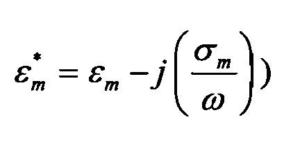 where fCM = ε* p - ε* m / ε* p + 2ε* m is the Clausius-Mosotti factor, α is the particle radius and ϕ is the electric field phase. So if the particle is more conductive than the medium around it, the dipole aligns with the field and the force acts up the field gradient towards the region of highest electric field.
- On the contrary if the particle is less polarizable than the medium, the dipole aligns against the field and particle is repelled from the regions of high electric field. So the force is unaffected by the direction of the electric field, responding only to the field gradient. Since the alignment of the field is irrelevant one could generate the electric field in AC, with the advantage of reducing any electrophoretic force, due to any net particle charge, to zero.
- It's worth noting that magnitude of
F DEP depends on the frequency of the AC electric field, since real and imaginary part of fCM are very different according to the work frequency (as can be shown in Figure 8). It's useful to set the working frequency so as to choose the weight of each of the two contributes of the force, linked to the real or the imaginary part. - So, as result, the real component of fCM is usually used to trap the particle, while the imaginary component is for translational particle actuation. The field induced force increases as field gradient becomes stronger. An increase of field gradient can be obtained by miniaturization of the electrodes.
- To develop a model in order to control the migration process, in the balance of applied forces it must be considered also the Stokes friction force due to the viscosity of the host fluid as result of the motion of a sphere in it:
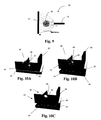
- A schematic view of a polarizable particle suspended within a point-plane electrode system is shown in Figure 9. The
system 30 includes aplane electrode 32 and apoint electrode 34 with aparticle 36 between the electrodes. When theparticle 36 polarizes, the interaction between the dipolar charges with the local electric field produces a force. - Due to the inhomogeneous nature of the electric field, the force is greater in the side facing the
point electrode 34 than that on the side facing theplane electrode 32, and there is net motion of theparticle 36 towards thepoint electrode 34. This effect is called positive dielectrophoresis. If theparticle 36 is less polarizable than the surrounding medium, the dipole of theparticle 36 will align in opposition with respect to the electric field and theparticle 36 will be repelled from the high field regions. This effect is called negative dielectrophoresis. - Then, the method according to the invention further comprises a phase of realization of a nanocontact.
- In fact, before the nanowire synthesis phase, it is necessary to realize a nanocontact, whose target offers a reference point for the growth of the nanowire as well the electrode towards which the nanoclusters move under the control of the electric field, as shown in figures 10A to 10C. The nanocontact realization phase comprises in turn:
- a
substrate 40 is processed to be patterned, for instance by lithography, to obtain ametallic layer 42 between twooxide layers free face 48 available for electro-deposition; - when an electric field is applied between a
flat panel 50 and the metallicfree face 48, a passivatednanocluster 52, whose sizes are comparable to the thickness of themetallic layer 42, moves to thefree face 48, under dielectrophoresis, with the thioles S-H group linked to it; - the
substrate 40 is then heated by aheater 54 until the thioles degradation temperature is reached; when this occurs the dielectric shell realized by the thioles, surrounding the metal core of thenanocluster 52, vanishes leaving a nanoparticle ornanocontact 56 that finds stability joining thefree face 48. - The thioles degradation may be performed even by UV treatment.
- However, the process may even not require a treatment for thioles degradation since in case of very thin thioles barriers (about nm) the tunneling effect could assure a significant conduction.
- The so-created
nanocontact 56 is the new reference point for the others nanoclusters 52 since the force lines of the electric field get denser close to a smaller radius curvature region such as the nanocontact itself, as shown in figures 11 A and 11 B. - In this new configuration others
smaller nanoclusters 52 join together as an one-dimensional array; then a new heating produces the degradation of the thioles shells and ananowire 58 is formed. - In other words, under control of a non homogeneous electric field the metallic passivated nanoclusters are forced to assembly.
- It must be noted that, according to the present invention, metallic nanoclusters could be deposited for catalytic applications, in such a way to realize catalytic material by a dielectric deposition. A possible application for these kind of metallic nanoclusters is the growing of nano-tubes or the use as catalytic loads in polimeric electrodes.
- Starting from the above method for realizing a nanowire, a method for producing a SE device is also described, with reference to figures 12 and 13.
- Advantageously according to the present invention, the method for producing a SE device, comprises a first step of patterning of a substrate, as already described above with reference to figures 5A-5C.
- After having dipped the patterned substrate in a solution containing metallic passivated nanoclusters, a
flat electrode 60 is suspended parallel to the patterned substrate without contacting it, as can be seen in Figure 12. Also shown in figure 13 is an enlarged view of acentral aperture 14 of the patterned substrate, wherein North, East, South and West electrodes (respectively indicated as 62, 64, 66 and 68) formed in thepaths 16 are highlighted. - In the preferred embodiment shown in Figure 13, the
central aperture 14 is rectangular and theelectrodes - The distance between the
electrode 60 and the patterned substrate is one of the design parameters which allows to control the curvature of the force lines of the electric field and so the dielectrophoresis force as well as the potential applied to it. In details, a potential difference is applied between the fourelectrodes electrodes electrodes central aperture 14. - In this way metallic nanoclusters are obliged to migrate towards the free faces of the four
electrodes - Advantageously, according to the present invention, the metallic passivated
nanoclusters 52 are forced to assembly under control of a non homogeneous electric field, said process step being performed at room temperature. - So, using the patterned substrate shown in figure 13 and applying an electric field by means of the
plate electrode 60, a first and a second nanowires, aligned with the perpendicular directions N-S and W-E defined by the fourelectrodes - However, the ability to control precisely the process of self-assembly nanoclusters is depending on the uniformity of the electric field between the
top electrode 60, acting as flat panel, and the fourelectrodes - So, advantageously according to the invention, before the dielectrophoresis process, an integrated microcavity is realized in order to guarantee the possibility to act a fine control of the distance dz between the
top electrode 60 and the patterned substrate as well as the control of its shape, and so in order to precisely control the nanowire assembly. - A typical example of process flow-chart to build up the integrate
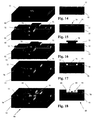
microcavity 82 as well as an integratedtop electrode 60 is reported in the scheme sequence of Figures 14-18, which is only intended as a possible realization scheme not exhaustive of the possible alternative realizations. - The process of Figures 14-18 begins similarly to the process of Figures 5A-5C with the formation of a thin silicon oxide layer (SiO2) 12 on a silicon (Si)
substrate 10 as shown in Figure 14. Then, instead of etching acentral aperture 14 andcontact pads 16 in thesilicon oxide layer 12, as in Figures 5A-5C, advantageously according to the invention, the process comprises a step of depositing aluminum orother metal contacts 72 on thesilicon oxide layer 12, in such a way to form a central aperture 74 (which correspond to thecentral aperture 14 of Figure 13) between themetal contacts 72, as shown in Figure 15. - The process further comprises a step of forming a silicon nitride
sacrifical layer 76 in such a way to fill thecentral aperture 74 and to cover at least portions of themetal contact 72, as shown in Figure 16. - The thin
silicon oxide layer 12 is then grown to form a thicksilicon oxide layer 78 laterally of the silicon nitridesacrifical layer 76 and on themetal contacts 72, as shown in Figure 17. - The process still further comprises a step of removing the silicon nitride
sacrifical layer 76 so forming theintegrated microcavity 82. - Then , the process comprises a step of forming a
plate electrode 60 on the thicksilicon oxide layer 78 and above thecentral aperture 74, so closing themicrocavity 82, as shown in Figure 18. - Finally, the process comprises a phase of forming
nanowires 70 within the integratedmicrocavity 82 according to the dielectrophoretic process described above with reference of Figures 12 and 13, so obtaining a complete single electron (SE)structure 80. - It should be noted that, advantageously, the
central aperture 14 in the patterned substrate is chosen rectangular in order to have, for example, a distance between theN-S electrodes nanowires 70 of different lengths are obtained, as shown in Figure 13. In particular, the WE electrodes distance is chosen of the order of 10nm. - A typical size for the
central aperture 14 of the microcavity is 90x150nm2 (that can be obtained for instance by conventional lithography techniques) and 30nm for electrodes width so that, if thenanowires 70 are developed with a final length of about 40nm, it will results in a W-E electrodes distance of about 10nm and a N-S electrodes distance of about 70nm. - Advantageously according to the invention, the gap between the so obtained
nanowires 70 starting from theelectrodes plate electrode 60 lets a nanocluster occupy such a nanowires gap, so obtaining acomplete SE structure 80, as shown in figure 18. - This
structure 80 including four terminal electrodes (62, 64, 66, 68) may be used, for example, as an AND/OR logic gate. - Analogously, the process can easy be extended to integrate more than one Single Electron (SE) Devices in a single microcavity as well as to integrate both SE devices with conventional components and circuits (for example to integrate the signal amplifiers and conditioning circuits, as well as to develop a buried resistor grid which will act as the heater for the thioles degradation in the final steps of the nanowires realization).
- So, as shown in figures 5A-5C and 18, the invention also relates to a single electron device comprising a quantum dot as single electron component housed on a patterned
substrate nanowire 70 to the quantum dot. - In particular, the single electron device, shown in the figures as a preferred embodiment of the present invention, comprises a plurality of
electrodes nanowires 70 to the quantum dot, the gap between thenanowires 70 defining a location for the quantum dot, as explained above. - Advantageously, the quantum dot is realized by a metallic passivated
nanocluster 52, according to the present invention. - Also, the single electron device according to the present invention includes a
microcavity 82 having acentral aperture electrodes nanowires 70 as well as the quantum dot. - All these possibilities are intended as an extension of the basic idea, suitable to develop a hybrid nanotechnology and nanofabrication approach to develop novel SE-based circuits working at room temperature.
- It is worth noting that from the basic four-electrodes patterned substrate it is possible to build up SE devices of different kind depending on the material used to realize either the four nanowires or the quantum dot.
- Then possible choices involve the employment of metallic CNT or any organic conductive material (polythiophene based-molecules) as nanowires, while as quantum dot one could use either a metallic or semiconductive material according to the desired properties and applications. Another possible choice, for the quantum dot, involves the use of treated carbon structures (C60 based molecules) or Si clusters surrounded by a SiO2 dielectric shell.
- The method of the present invention does solve the technical problem and achieves various advantages and benefits.
- An important benefit of this process is the possibility to realize controllable length and width nanowires overcoming the limits of the prior art techniques. The invention also allows the development of new family of nanoelectronic devices easily and cheaply.
- Employing this technique one can build up basic single-electron devices (SE-box, SE-transistor, SE Turnstile and pump, SE transistor oscillators), analog application (supersensitive electrometry, SE spectroscopy, CD current standards, temperature standards, resistance standards, detection of infrared radiation) and digital application (voltage state logics, charge state logics, SET/FET memory, NOVAROM).
- The proposed structure can be used either as a SET device, driving both the gate electrodes with the same control signal, or as a logic gate, driving each gate electrode with a suitable digital signal. In particular the latter can be used either as an OR or as an AND gate, depending on the signal value applied at each gate electrode.
- From the foregoing it will be appreciated that, although specific embodiments of the invention have been described herein for purposes of illustration, various modifications may be made without departing from the scope of the invention as defined in the annexed claims.
Claims (31)
- Method for manufacturing a single electron device (80) by electro-migration of nanoclusters (52) characterized in that it comprises the steps of:patterning a substrate (10, 40);preparing metallic passivated nanoclusters (52);forcing said metallic passivated nanoclusters (52) to assembly over said patterned substrate (10) under control of a non homogeneous electric field.
- Method according to claim 1 characterized in that said step of forcing said metallic passivated nanoclusters (52) comprises a dielectrophoretic process.
- Method according to claim 1 characterized in that said step of forcing said metallic passivated nanoclusters (52) is performed at room temperature.
- Method according to claim 1 characterized in that said step of preparing metallic passivated nanoclusters (52) includes the following steps:synthesis of active metal;superficial passivation of said active metal with thiol;extraction and purification of said metallic nanoclusters (52).
- Method according to claim 4 characterized in that said step of synthesis of active metal comprises a polyol process used to prepare finely divided powders of easily reducible metals.
- Method according to claim 5 characterized in that said polyol process comprises a reaction mechanism in two stages as follows:1 st stagedissolving a starting metal compound in a polyol in order to form a first solution;precipitating an intermediate phase from said first solution;removing water by distillation from said intermediate phase.2nd stagedissolving said intermediate phase in a polyol to form a second solution;reducing said intermediate phase in said second solution;allowing volatile reaction products to evolve from said second solution;spontaneous nucleating and growing metal nanoclusters (52) from said second solution.
- Method according to claim 6 characterized in that said starting metal compound is chosen by the group comprising: metal hydroxides, metal oxides or metal salts.
- Method according to any one of the claims 5-7 characterized in that said polyol is chosen between ethylene glycol (EG) and diethylene glycol (DEG).
- Method according to claim 4 characterized in that the step of superficial passivation of said active metal with thiol comprises the following steps:suspending said metallic nanoclusters (52) in a third solution; andadding thiol compounds to said third solution in such a way that thiol molecules are chemically absorbed to the nanoclusters (52) surface.
- Method according to claim 9 characterized in that said thiol compounds are dodecanthiol (CH3(CH2)11SH) or a thiol excess having the formula: CH3(CH2)nSH, where n is an integer.
- Method according to claim 9 characterized in that said third solution comprises polyvinylpyrrolidone (PVP) as reducing agent and inhibitor of an aggregation process of the nanoclusters (52).
- Method according to claim 4 characterized in that said step of extraction comprises an extraction of said metallic nanoclusters (52) using hydrocarbon (wet-way process).
- Method according to claim 4 characterized in that said step of extraction comprises an addition of water followed by filtration (dry-way process).
- Method according to claim 4 characterized in that said step of purification is conducted by dissolving said extracted metallic nanoclusters (52) in ethyl alcohol, adding acetone to precipitate said metallic nanoclusters (52), separating said metallic nanoclusters (52) by centrifugation and drying said metallic nanoclusters (52) to the air.
- Method according to claim 4 characterized in that said step of forcing said metallic passivated nanoclusters (52) to assembly over said patterned substrate (10, 40) realizes at least one nanowire (70).
- Method according to claim 15 characterized in that said step of realizing said at least one nanowire (70) comprises the following steps:realizing at least one nanocontact (56) in said patterned substrate (10, 40);using said nanocontact (56) as a target that offers a reference point for growing said nanowire (70) by moving said metallic passivated nanoclusters (52) under the control of said non homogeneous electric field.
- Method according to claim 16 characterized in that said step of realizing said nanocontact (56) comprises the steps of:patterning said substrate (10, 40) in order to obtain a metallic layer (42) between two oxide layers (44, 46) with a free face (48) available for electro-deposition;applying said non homogeneous electric field between a plate electrode (50, 60) and said free face (48) in order to mode said metallic passivated nanoclusters (52) toward said free face (48);heating said metallic passivated nanoclusters (52) to remove said passivation and obtain said nanocontact (56) joining said free face (48).
- Method according to claim 17 characterized in that said step of patterning said substrate (10, 40) further includes the realization of a plurality of electrodes (62, 64, 66, 68) surrounding a central aperture (14, 74).
- Method according to claim 18 characterized in that said central aperture (14, 74) is rectangular and said electrodes (62, 64, 66, 68) are substantially central located with respect to the central aperture sides.
- Method according to claim 18 characterized in that it further comprises a step of applying a potential difference is applied between four electrodes (62, 64, 66, 68), held to a same potential and a plate electrode (60) in order to oblige said metallic passivated nanoclusters (52) to migrate towards the free faces of said electrodes (62, 64, 66, 68) and to self-assembly in a direction perpendicular to those faces, so forming a plurality of nanowires (70).
- Method according to claim 16 characterized in that said step of patterning said substrate (10, 40) further realizes an integrated microcavity (82).
- Method according to claim 21 characterized in that said integrated microcavity (82) is realized by the following steps:forming a thin silicon oxide layer (12) on a silicon substrate (10);depositing metal contacts (72) on said silicon oxide layer (12), in such a way to form a central aperture (74) between said metal contacts (72);forming a sacrifical layer (76) in such a way to fill said central aperture (74) and to cover at least portions of said metal contacts (72);growing said thin silicon oxide layer (12) to form a thick silicon oxide layer (78) laterally of said sacrifical layer (76) and on said metal contacts (72);removing said sacrifical layer (76) so forming said integrated microcavity (82).
- Method according to claim 22 characterized in that it further comprises a step of forming said plate electrode (60) on said thick silicon oxide layer (78) and above said central aperture (74), so closing said integrated microcavity (82).
- Method according to claim 21 characterized in that said nanowires (70) are formed within said integrated microcavity (82).
- Method according to claim 20 characterized in that said step of forming said nanowires (70) leaves a gap between the nanowires (70) defining a location for a quantum dot as single electron components.
- Method according to claim 25 characterized in that said step of applying said non homogeneous electric field lets a nanocluster occupy said gap as a quantum dot.
- Single electron device comprising a quantum dot as single electron component housed on a patterned substrate (10, 40) which includes at least an electrode (62, 64, 66, 68), characterized in that said electrode (62, 64, 66, 68) is connected by at least a nanowire (70) to said quantum dot.
- Single electron device according to claim 27, characterized in that said quantum dot is realized by a metallic passivated nanocluster (52).
- Single electron device according to claim 27, characterized in that it comprises a plurality of electrodes (62, 64, 66, 68) connected by a plurality of nanowires (70) to said quantum dot and in that said plurality of nanowires (70) have a gap defining a location for said quantum dot.
- Single electron device according to claim 27, characterized in that said patterned substrate (10, 40) includes microcavity (82) having a central aperture (14, 74) surrounded by the electrodes (62, 64, 66, 68).
- Single electron device according to claim 30, characterized in that said nanowires (70) and said quantum dot are housed in said microcavity (82).
Applications Claiming Priority (2)
| Application Number | Priority Date | Filing Date | Title |
|---|---|---|---|
| US695479 | 2003-10-28 | ||
| US10/695,479 US7067341B2 (en) | 2003-10-28 | 2003-10-28 | Single electron transistor manufacturing method by electro-migration of metallic nanoclusters |
Publications (1)
| Publication Number | Publication Date |
|---|---|
| EP1528039A1 true EP1528039A1 (en) | 2005-05-04 |
Family
ID=34423354
Family Applications (1)
| Application Number | Title | Priority Date | Filing Date |
|---|---|---|---|
| EP04025635A Withdrawn EP1528039A1 (en) | 2003-10-28 | 2004-10-28 | Method for manufacturing a single electron device by electro-migration of nanoclusters and corresponding single electron device |
Country Status (2)
| Country | Link |
|---|---|
| US (1) | US7067341B2 (en) |
| EP (1) | EP1528039A1 (en) |
Cited By (4)
| Publication number | Priority date | Publication date | Assignee | Title |
|---|---|---|---|---|
| WO2007017401A3 (en) * | 2005-08-11 | 2007-04-19 | Siemens Ag | Method for integrating functional nanostructures into microelectric and nanoelectric circuits |
| WO2009108404A3 (en) * | 2008-01-11 | 2009-11-05 | The Penn State Research Foundation | Bottom-up assembly of structures on a substrate |
| WO2010000689A1 (en) * | 2008-07-04 | 2010-01-07 | Siemens Aktiengesellschaft | Sensor device for measuring an electric field and method for the manufacture thereof |
| WO2012035194A1 (en) * | 2010-09-15 | 2012-03-22 | Nokia Corporation | An apparatus and associated methods |
Families Citing this family (23)
| Publication number | Priority date | Publication date | Assignee | Title |
|---|---|---|---|---|
| US7651926B2 (en) * | 2002-05-24 | 2010-01-26 | Massachusetts Institute Of Technology | Rapid patterning of nanostructures |
| US8093144B2 (en) * | 2002-05-24 | 2012-01-10 | Massachusetts Institute Of Technology | Patterning of nanostructures |
| WO2006076036A2 (en) * | 2004-05-25 | 2006-07-20 | The Trustees Of The University Of Pennsylvania | Nanostructure assemblies, methods and devices thereof |
| US8039368B2 (en) * | 2005-03-21 | 2011-10-18 | The Trustees Of The University Of Pennsylvania | Nanogaps: methods and devices containing same |
| US7567138B2 (en) * | 2006-08-29 | 2009-07-28 | Texas Instruments Incorporated | Single-electron injection/extraction device for a resonant tank circuit and method of operation thereof |
| GB0625070D0 (en) * | 2006-12-15 | 2007-01-24 | Imp Innovations Ltd | Characterization of molecules |
| GB0708381D0 (en) * | 2007-04-30 | 2007-06-06 | Nokia Corp | Method for forming a semiconductor structure |
| US20090038832A1 (en) * | 2007-08-10 | 2009-02-12 | Sterling Chaffins | Device and method of forming electrical path with carbon nanotubes |
| US7922787B2 (en) * | 2008-02-02 | 2011-04-12 | Seashell Technology, Llc | Methods for the production of silver nanowires |
| EP2319060A1 (en) * | 2008-08-26 | 2011-05-11 | Nxp B.V. | A capacitor and a method of manufacturing the same |
| US8013324B2 (en) * | 2009-04-03 | 2011-09-06 | International Business Machines Corporation | Structurally stabilized semiconductor nanowire |
| US7902541B2 (en) * | 2009-04-03 | 2011-03-08 | International Business Machines Corporation | Semiconductor nanowire with built-in stress |
| US7943530B2 (en) * | 2009-04-03 | 2011-05-17 | International Business Machines Corporation | Semiconductor nanowires having mobility-optimized orientations |
| US8237150B2 (en) * | 2009-04-03 | 2012-08-07 | International Business Machines Corporation | Nanowire devices for enhancing mobility through stress engineering |
| US8368125B2 (en) | 2009-07-20 | 2013-02-05 | International Business Machines Corporation | Multiple orientation nanowires with gate stack stressors |
| US20110012177A1 (en) * | 2009-07-20 | 2011-01-20 | International Business Machines Corporation | Nanostructure For Changing Electric Mobility |
| CN102169837B (en) * | 2011-03-12 | 2013-05-01 | 中国科学院苏州纳米技术与纳米仿生研究所 | Preparation method of single electron transistor at room temperature |
| CN103022346B (en) * | 2011-09-27 | 2014-09-10 | 华邦电子股份有限公司 | Resistance-type memorizer |
| WO2013072568A1 (en) * | 2011-11-16 | 2013-05-23 | Arutyunov Konstantin Yurievich | Nanostructure and method for determining a dc electric current |
| CN102517640A (en) * | 2011-12-12 | 2012-06-27 | 大连理工大学 | Method for in situ growth of metal oxide, metal nitride and metal carbide nanowires |
| WO2014052887A2 (en) | 2012-09-27 | 2014-04-03 | Rhodia Operations | Process for making silver nanostructures and copolymer useful in such process |
| US10032897B2 (en) | 2016-06-01 | 2018-07-24 | International Business Machines Corporation | Single electron transistor with self-aligned Coulomb blockade |
| CN108109903A (en) * | 2017-11-22 | 2018-06-01 | 西交利物浦大学 | A kind of thiol treatment method of gallium nitride surface |
Citations (6)
| Publication number | Priority date | Publication date | Assignee | Title |
|---|---|---|---|---|
| EP0836232A1 (en) * | 1996-03-26 | 1998-04-15 | Samsung Electronics Co., Ltd. | Tunnelling device and method of producing a tunnelling device |
| EP0865078A1 (en) * | 1997-03-13 | 1998-09-16 | Hitachi Europe Limited | Method of depositing nanometre scale particles |
| US6313479B1 (en) * | 1999-09-14 | 2001-11-06 | Zhenyu Zhang | Self-organized formation of quantum dots of a material on a substrate |
| WO2003016209A1 (en) * | 2001-08-20 | 2003-02-27 | Nanocluster Devices Ltd. | Nanoscale electronic devices & fabrication methods |
| US20030048619A1 (en) * | 2001-06-15 | 2003-03-13 | Kaler Eric W. | Dielectrophoretic assembling of electrically functional microwires |
| US20030102444A1 (en) * | 2000-05-04 | 2003-06-05 | Deppert Knut Wilfried | Nanostructures |
Family Cites Families (4)
| Publication number | Priority date | Publication date | Assignee | Title |
|---|---|---|---|---|
| US6721083B2 (en) * | 1996-07-19 | 2004-04-13 | E Ink Corporation | Electrophoretic displays using nanoparticles |
| US6538801B2 (en) * | 1996-07-19 | 2003-03-25 | E Ink Corporation | Electrophoretic displays using nanoparticles |
| US6447887B1 (en) * | 1999-09-14 | 2002-09-10 | Virginia Tech Intellectual Properties, Inc. | Electrostrictive and piezoelectric thin film assemblies and method of fabrication therefor |
| US6579463B1 (en) * | 2000-08-18 | 2003-06-17 | The Regents Of The University Of Colorado | Tunable nanomasks for pattern transfer and nanocluster array formation |
-
2003
- 2003-10-28 US US10/695,479 patent/US7067341B2/en not_active Expired - Lifetime
-
2004
- 2004-10-28 EP EP04025635A patent/EP1528039A1/en not_active Withdrawn
Patent Citations (6)
| Publication number | Priority date | Publication date | Assignee | Title |
|---|---|---|---|---|
| EP0836232A1 (en) * | 1996-03-26 | 1998-04-15 | Samsung Electronics Co., Ltd. | Tunnelling device and method of producing a tunnelling device |
| EP0865078A1 (en) * | 1997-03-13 | 1998-09-16 | Hitachi Europe Limited | Method of depositing nanometre scale particles |
| US6313479B1 (en) * | 1999-09-14 | 2001-11-06 | Zhenyu Zhang | Self-organized formation of quantum dots of a material on a substrate |
| US20030102444A1 (en) * | 2000-05-04 | 2003-06-05 | Deppert Knut Wilfried | Nanostructures |
| US20030048619A1 (en) * | 2001-06-15 | 2003-03-13 | Kaler Eric W. | Dielectrophoretic assembling of electrically functional microwires |
| WO2003016209A1 (en) * | 2001-08-20 | 2003-02-27 | Nanocluster Devices Ltd. | Nanoscale electronic devices & fabrication methods |
Non-Patent Citations (1)
| Title |
|---|
| HORI M ET AL: "Sub-5 nm gold dot formation using retarding-field single ion deposition", APPLIED PHYSICS LETTERS, AMERICAN INSTITUTE OF PHYSICS. NEW YORK, US, vol. 73, no. 22, 30 November 1998 (1998-11-30), pages 3223 - 3225, XP012021519, ISSN: 0003-6951 * |
Cited By (4)
| Publication number | Priority date | Publication date | Assignee | Title |
|---|---|---|---|---|
| WO2007017401A3 (en) * | 2005-08-11 | 2007-04-19 | Siemens Ag | Method for integrating functional nanostructures into microelectric and nanoelectric circuits |
| WO2009108404A3 (en) * | 2008-01-11 | 2009-11-05 | The Penn State Research Foundation | Bottom-up assembly of structures on a substrate |
| WO2010000689A1 (en) * | 2008-07-04 | 2010-01-07 | Siemens Aktiengesellschaft | Sensor device for measuring an electric field and method for the manufacture thereof |
| WO2012035194A1 (en) * | 2010-09-15 | 2012-03-22 | Nokia Corporation | An apparatus and associated methods |
Also Published As
| Publication number | Publication date |
|---|---|
| US7067341B2 (en) | 2006-06-27 |
| US20050090081A1 (en) | 2005-04-28 |
Similar Documents
| Publication | Publication Date | Title |
|---|---|---|
| US7067341B2 (en) | Single electron transistor manufacturing method by electro-migration of metallic nanoclusters | |
| Likharev | Single-electron devices and their applications | |
| Ahmed | Single electron electronics: Challenge for nanofabrication | |
| Nakaharai et al. | Conduction tuning of graphene based on defect-induced localization | |
| Antonova | Vertical heterostructures based on graphene and other 2D materials | |
| Yakimov et al. | Hopping conduction and field effect in Si modulation-doped structures with embedded Ge quantum dots | |
| Karmakar et al. | Nano-electronics and spintronics with nanoparticles | |
| US10825920B2 (en) | Energy-filtered cold electron devices and methods | |
| Junno et al. | Single-electron devices via controlled assembly of designed nanoparticles | |
| WO2021191629A1 (en) | Fabrication method of a nanodevice with a nanogap electrode | |
| Fu et al. | Carrier conduction in a Si-nanocrystal-based single-electron transistor-I. Effect of gate bias | |
| Zheng et al. | Robust quantum oscillation of Dirac fermions in a single-defect resonant transistor | |
| Ramezani et al. | Fundamental phenomena in nanoscale semiconductor devices | |
| Rai et al. | Review on single electron transistor (SET): emerging device in nanotechnology | |
| Bagraev et al. | Local tunneling spectroscopy of silicon nanostructures | |
| Tilke et al. | Single-electron tunneling in silicon nanostructures | |
| Ramezani et al. | 1 Fundamental Phenomena | |
| Yakimov et al. | Germanium self-assembled quantum dots in silicon: growth, electronic transport, optical phenomena, and devices | |
| Zhao et al. | Electron Transport in Single Molecules and Nanostructures | |
| Haug | Single-electron tunneling through semiconducting nanostructures | |
| Luo | Electron transport in nanoparticle single-electron transistors | |
| JP2012190859A (en) | Resonant tunnel diode and manufacturing method thereof | |
| Guerin et al. | Coulomb blockade in a granular material made of gold nanowires | |
| Wong et al. | Local doping of two-dimensional materials | |
| Markert et al. | Electron Transport in Nanoparticle Single-Electron Transistors |
Legal Events
| Date | Code | Title | Description |
|---|---|---|---|
| PUAI | Public reference made under article 153(3) epc to a published international application that has entered the european phase |
Free format text: ORIGINAL CODE: 0009012 |
|
| AK | Designated contracting states |
Kind code of ref document: A1 Designated state(s): AT BE BG CH CY CZ DE DK EE ES FI FR GB GR HU IE IT LI LU MC NL PL PT RO SE SI SK TR |
|
| AX | Request for extension of the european patent |
Extension state: AL HR LT LV MK |
|
| AKX | Designation fees paid | ||
| REG | Reference to a national code |
Ref country code: DE Ref legal event code: 8566 |
|
| STAA | Information on the status of an ep patent application or granted ep patent |
Free format text: STATUS: THE APPLICATION IS DEEMED TO BE WITHDRAWN |
|
| 18D | Application deemed to be withdrawn |
Effective date: 20051105 |