EP1524652A1 - Optical recording medium, optical recording medium manufacturing method, and optical recording medium reproducing method - Google Patents
Optical recording medium, optical recording medium manufacturing method, and optical recording medium reproducing method Download PDFInfo
- Publication number
- EP1524652A1 EP1524652A1 EP04720984A EP04720984A EP1524652A1 EP 1524652 A1 EP1524652 A1 EP 1524652A1 EP 04720984 A EP04720984 A EP 04720984A EP 04720984 A EP04720984 A EP 04720984A EP 1524652 A1 EP1524652 A1 EP 1524652A1
- Authority
- EP
- European Patent Office
- Prior art keywords
- pits
- row
- recording medium
- reflection film
- substrate
- Prior art date
- Legal status (The legal status is an assumption and is not a legal conclusion. Google has not performed a legal analysis and makes no representation as to the accuracy of the status listed.)
- Granted
Links
Images


Classifications
-
- G—PHYSICS
- G11—INFORMATION STORAGE
- G11B—INFORMATION STORAGE BASED ON RELATIVE MOVEMENT BETWEEN RECORD CARRIER AND TRANSDUCER
- G11B7/00—Recording or reproducing by optical means, e.g. recording using a thermal beam of optical radiation by modifying optical properties or the physical structure, reproducing using an optical beam at lower power by sensing optical properties; Record carriers therefor
- G11B7/24—Record carriers characterised by shape, structure or physical properties, or by the selection of the material
- G11B7/241—Record carriers characterised by shape, structure or physical properties, or by the selection of the material characterised by the selection of the material
- G11B7/252—Record carriers characterised by shape, structure or physical properties, or by the selection of the material characterised by the selection of the material of layers other than recording layers
- G11B7/258—Record carriers characterised by shape, structure or physical properties, or by the selection of the material characterised by the selection of the material of layers other than recording layers of reflective layers
-
- G—PHYSICS
- G11—INFORMATION STORAGE
- G11B—INFORMATION STORAGE BASED ON RELATIVE MOVEMENT BETWEEN RECORD CARRIER AND TRANSDUCER
- G11B7/00—Recording or reproducing by optical means, e.g. recording using a thermal beam of optical radiation by modifying optical properties or the physical structure, reproducing using an optical beam at lower power by sensing optical properties; Record carriers therefor
- G11B7/007—Arrangement of the information on the record carrier, e.g. form of tracks, actual track shape, e.g. wobbled, or cross-section, e.g. v-shaped; Sequential information structures, e.g. sectoring or header formats within a track
- G11B7/00736—Auxiliary data, e.g. lead-in, lead-out, Power Calibration Area [PCA], Burst Cutting Area [BCA], control information
-
- G—PHYSICS
- G11—INFORMATION STORAGE
- G11B—INFORMATION STORAGE BASED ON RELATIVE MOVEMENT BETWEEN RECORD CARRIER AND TRANSDUCER
- G11B7/00—Recording or reproducing by optical means, e.g. recording using a thermal beam of optical radiation by modifying optical properties or the physical structure, reproducing using an optical beam at lower power by sensing optical properties; Record carriers therefor
- G11B7/004—Recording, reproducing or erasing methods; Read, write or erase circuits therefor
- G11B7/005—Reproducing
-
- G—PHYSICS
- G11—INFORMATION STORAGE
- G11B—INFORMATION STORAGE BASED ON RELATIVE MOVEMENT BETWEEN RECORD CARRIER AND TRANSDUCER
- G11B7/00—Recording or reproducing by optical means, e.g. recording using a thermal beam of optical radiation by modifying optical properties or the physical structure, reproducing using an optical beam at lower power by sensing optical properties; Record carriers therefor
- G11B7/004—Recording, reproducing or erasing methods; Read, write or erase circuits therefor
- G11B7/005—Reproducing
- G11B7/0053—Reproducing non-user data, e.g. wobbled address, prepits, BCA
-
- G—PHYSICS
- G11—INFORMATION STORAGE
- G11B—INFORMATION STORAGE BASED ON RELATIVE MOVEMENT BETWEEN RECORD CARRIER AND TRANSDUCER
- G11B7/00—Recording or reproducing by optical means, e.g. recording using a thermal beam of optical radiation by modifying optical properties or the physical structure, reproducing using an optical beam at lower power by sensing optical properties; Record carriers therefor
- G11B7/007—Arrangement of the information on the record carrier, e.g. form of tracks, actual track shape, e.g. wobbled, or cross-section, e.g. v-shaped; Sequential information structures, e.g. sectoring or header formats within a track
-
- G—PHYSICS
- G11—INFORMATION STORAGE
- G11B—INFORMATION STORAGE BASED ON RELATIVE MOVEMENT BETWEEN RECORD CARRIER AND TRANSDUCER
- G11B7/00—Recording or reproducing by optical means, e.g. recording using a thermal beam of optical radiation by modifying optical properties or the physical structure, reproducing using an optical beam at lower power by sensing optical properties; Record carriers therefor
- G11B7/24—Record carriers characterised by shape, structure or physical properties, or by the selection of the material
- G11B7/26—Apparatus or processes specially adapted for the manufacture of record carriers
-
- G—PHYSICS
- G11—INFORMATION STORAGE
- G11B—INFORMATION STORAGE BASED ON RELATIVE MOVEMENT BETWEEN RECORD CARRIER AND TRANSDUCER
- G11B7/00—Recording or reproducing by optical means, e.g. recording using a thermal beam of optical radiation by modifying optical properties or the physical structure, reproducing using an optical beam at lower power by sensing optical properties; Record carriers therefor
- G11B7/24—Record carriers characterised by shape, structure or physical properties, or by the selection of the material
- G11B7/26—Apparatus or processes specially adapted for the manufacture of record carriers
- G11B7/268—Post-production operations, e.g. initialising phase-change recording layers, checking for defects
-
- G—PHYSICS
- G11—INFORMATION STORAGE
- G11B—INFORMATION STORAGE BASED ON RELATIVE MOVEMENT BETWEEN RECORD CARRIER AND TRANSDUCER
- G11B20/00—Signal processing not specific to the method of recording or reproducing; Circuits therefor
- G11B20/00086—Circuits for prevention of unauthorised reproduction or copying, e.g. piracy
- G11B20/0021—Circuits for prevention of unauthorised reproduction or copying, e.g. piracy involving encryption or decryption of contents recorded on or reproduced from a record carrier
- G11B20/00217—Circuits for prevention of unauthorised reproduction or copying, e.g. piracy involving encryption or decryption of contents recorded on or reproduced from a record carrier the cryptographic key used for encryption and/or decryption of contents recorded on or reproduced from the record carrier being read from a specific source
- G11B20/00253—Circuits for prevention of unauthorised reproduction or copying, e.g. piracy involving encryption or decryption of contents recorded on or reproduced from a record carrier the cryptographic key used for encryption and/or decryption of contents recorded on or reproduced from the record carrier being read from a specific source wherein the key is stored on the record carrier
- G11B20/0026—Circuits for prevention of unauthorised reproduction or copying, e.g. piracy involving encryption or decryption of contents recorded on or reproduced from a record carrier the cryptographic key used for encryption and/or decryption of contents recorded on or reproduced from the record carrier being read from a specific source wherein the key is stored on the record carrier the key being stored as a barcode
- G11B20/00268—Circuits for prevention of unauthorised reproduction or copying, e.g. piracy involving encryption or decryption of contents recorded on or reproduced from a record carrier the cryptographic key used for encryption and/or decryption of contents recorded on or reproduced from the record carrier being read from a specific source wherein the key is stored on the record carrier the key being stored as a barcode said barcode being recorded in a burst cutting area [BCA]
-
- G—PHYSICS
- G11—INFORMATION STORAGE
- G11B—INFORMATION STORAGE BASED ON RELATIVE MOVEMENT BETWEEN RECORD CARRIER AND TRANSDUCER
- G11B7/00—Recording or reproducing by optical means, e.g. recording using a thermal beam of optical radiation by modifying optical properties or the physical structure, reproducing using an optical beam at lower power by sensing optical properties; Record carriers therefor
- G11B7/24—Record carriers characterised by shape, structure or physical properties, or by the selection of the material
- G11B7/2407—Tracks or pits; Shape, structure or physical properties thereof
- G11B7/24073—Tracks
- G11B7/24079—Width or depth
Definitions
- the present invention relates to an optical recording medium, particularly, an optical disk which is shaped like a circular plate and is used to reproduce information.
- an optical disk such as a CD-ROM and a DVD-ROM.
- an uneven row of pits is formed on a transparent substrate which is made of polycarbonate or the like.
- a metal reflection film is formed which is made of Al or the like. From the side of the surface opposite to the surface on which this metal reflection film is formed, a beam of light is applied to the metal reflection film which is an information recording surface. Thereby, information is reproduced.
- Such an optical recording medium has been widely used in which information is recorded and reproduced by applying a beam of light.
- expectations have become greater of heightening its recording density from now on.
- a variety of optical disks have been developed which can reproduce large-capacity audio-visual data or digital data.
- research and development for a high-density ROM optical disk is now going on, in which the density of an optical disk which has a diameter of 12 centimeters is expected to become higher to a storage capacity of 23.3 to 30 gigabits.
- a DVD ROM recording medium is provided with a security technique, specifically, the technique of preventing someone from illicitly using and copying recorded information or from doing such an act.
- a security technique specifically, the technique of preventing someone from illicitly using and copying recorded information or from doing such an act.
- a BCA (or burst cutting area) area is provided where medium identification information which is used to identify each recording medium individually is overwritten in a bar-code pattern.
- medium identification information which differs for each optical recording medium is recorded, and if necessary, a key of cryptograph or a key of decoding is recorded.
- Japanese Patent Laid-Open No. 10-233019 specification discloses that a metal reflection film of an optical disk on which a row of pits is formed as main data is partially removed by a laser trimming, and modulated data is recorded individually.
- medium identification information is recorded which is used to protect against illicitly using and copying, or such an act.
- the pitch between tracks has to be narrowed, or the shortest pit of a row of pits needs to be shortened.
- 23.3 GB or more data is recorded on a 12cm-diameter optical disk. Therefore, it has been found out that if on a substrate used for such an optical disk, a metal reflection film is formed which is made of an Al alloy material having a film thickness of 50 to 70nm so that it can be used in a DVD ROM optical disk, that deteriorates the quality of a reproduced signal.
- An optical recording medium which includes a main-information area in which a metal reflection film is formed on a substrate where a row of pits is formed as main data, and a sub-information area in which medium identification information is recorded which is used to identify the optical recording medium individually by removing the metal reflection film partially and forming a plurality of reflection-film removed areas; and in which information is reproduced by irradiating the metal reflection film with a beam of light, where in the sub-information area, a row of pits or a groove is formed on the substrate, and the track pitch of the row of pits or the groove is 0.24 ⁇ m or wider and 0.45 ⁇ m or narrower.
- this optical recording medium a row of pits or a groove is formed in the sub-information area on the substrate, and the track pitch of the row of pits or the groove is set at 0.24 ⁇ m or wider and 0.45 ⁇ m or narrower. Therefore, using a beam of light for reproduction having a shorter wavelength and an optical system having a higher numerical aperture, data can be recorded at a higher density than in a DVD ROM optical disk. In addition, even though the thermal conductivity or melting point which is the intrinsic value of the metal reflection film is different, using a conventional medium-identification-information recording apparatus, medium identification information can be recorded so that an adequate defocus margin can be secured.
- a manufacturing method for an optical recording medium including: a first step of preparing a substrate on which a row of pits is formed as main data in a main-information area, and a row of pits or a groove whose track pitch is 0.24 ⁇ m or wider and 0.45 ⁇ m or narrower is formed in a sub-information area; a second step of forming a metal reflection film on the substrate; a third step of forming a resin layer on the metal reflection film; and a fourth step of recording medium identification information which is used to identify the optical recording medium individually by partially removing the metal reflection film in the sub-information area and forming a plurality of reflection-film removed areas.
- the row of pits or the groove is formed in the sub-information area on the substrate, and the track pitch of the row of pits or the groove is set at 0.24 ⁇ m or wider and 0.45 ⁇ m or narrower. Therefore, using a beam of light for reproduction having a shorter wavelength and an optical system having a higher numerical aperture, data can be recorded at a higher density than in a DVD ROM optical disk. In addition, even though the thermal conductivity or melting point which is the intrinsic value of the metal reflection film is different, using a conventional medium-identification-information recording apparatus, medium identification information can be recorded so that an adequate defocus margin can be secured.
- the optical recording medium includes a main-information area in which a metal reflection film is formed on a substrate where a row of pits is formed as main data, and a sub-information area in which a row of pits or a groove whose track pitch is 0.24 ⁇ m or wider and 0.45 ⁇ m or narrower is formed on the substrate, and medium identification information is recorded which is used to identify the optical recording medium individually by removing the metal reflection film partially and forming a plurality of reflection-film removed areas; and information is reproduced by irradiating the metal reflection film of the optical recording medium with a beam of light.
- an optical recording medium which is applied according to the present invention is not limited especially to this example.
- the present invention can also be applied to various optical recording mediums whose information recording layer has, for example, a minute unevenness, such as an optical magnetic disk and a phase-change disk.
- the ROM optical disk includes: a main-information area in which a metal reflection film is formed on a substrate where an uneven row of pits is formed as main data; and a sub-information area in which medium identification information is recorded which is used to identify the optical disk individually by removing the metal reflection film partially and forming a plurality of reflection-film removed areas.
- information is reproduced by irradiating the metal reflection film with a beam of light.
- the pitch between tracks has to be narrowed, and the shortest pit length (or the shortest mark length) needs to be extremely shortened.
- the track pitch becomes too narrow, cross talk becomes greater in an RF-signal characteristic. This hinders securing an adequate system margin. If the shortest pit length becomes too short, then the resolution of a reproduced signal lowers, thereby worsening the jitter value of the reproduced signal.
- a jitter value which shows characteristics of an optical disk needs to be 6.5% or below.
- a relational expression (shortest pit length) ⁇ (track pitch) ⁇ 0.0512 ⁇ m 2 has to be satisfied.
- the upper limit of the track pitch is about 0.43 ⁇ m.
- the upper limit of the track pitch is about 0.21 ⁇ m.
- a manufacturing method will be described of a 12cm-diameter optical disk which has a recording capacity of 23.3GB or above.
- a substrate has to be used whose track pitch is 0.24 ⁇ m or wider and 0.43 ⁇ m or narrower, and its shortest pit length is 0.12 ⁇ m or longer and 0.21 ⁇ m or shorter.
- a substrate is prepared where a row of pits is formed which has a shortest pit length of 0.149 ⁇ m and a track pitch of 0.32 ⁇ m.
- a substrate made of polycarbonate can be used which is created by an injection molding machine.
- a metal reflection film is formed on this substrate, using a film formation apparatus.
- the film formation apparatus the one which can form a metal reflection film uniformly, such as a magnetron sputtering apparatus and a vapor depositing apparatus, can be used.
- the time for film formation can be varied, thereby controlling the film thickness of the metal reflection film.
- the material, film thickness, or the like, of the metal reflection film will be described later.
- the optical disk is placed on a spin coater, with the metal reflection film kept up. Then, a resin to be hardened by ultraviolet rays is dripped, and on top of it, an 88 ⁇ m-thick transparent sheet which is made of polycarbonate is placed. In this state, the ultraviolet-ray hardened resin is irradiated with ultraviolet rays while the optical disk is being rotated by the spin coater. At this time, the rotational speed of the spin coater is controlled, so that the thickness of the ultraviolet-ray hardened resin after it has hardened becomes 12 ⁇ m. As a result, a transparent resin layer which has a film thickness of 100 ⁇ m is formed on the metal reflection film. For example, an acrylic resin can be used as this ultraviolet-ray hardened resin.
- the metal reflection film was formed on the substrate where the row of pits was formed which had a shortest pit length of 0.149 ⁇ m and a track pitch of 0.32 ⁇ m.
- the resin layer which had a film thickness of 100 ⁇ m is formed, and consequently, an optical disk is manufactured.
- the manufactured optical disk was set in the above described information reproducing apparatus. Then, this information reproducing apparatus allowed a beam of light to be incident upon the metal reflection film through the 100 ⁇ m-thick resin layer. Thereby, a reproduced signal was obtained from the optical disk, and then, it was assessed.
- Fig. 1 is a graphical representation, showing a measurement result of the value of a jitter which corresponds to the depth of a pit. Its horizontal axis is the depth (nm) of a pit and the vertical axis is the value (%) of a jitter.
- the metal reflection film the one was used which was made of an Al alloy with a purity of 99wt% and had a film thickness of 25nm.
- the AgPdCu alloy even when the one which was made of an Ag98Pd1Cu1(wt%) (hereinafter, referred to as the AgPdCu alloy), the same result as the following was obtained.
- a jitter has to be 6.5% or below.
- a refractive index n of the created resin layer was 1.53, and a wavelength ⁇ of the beam of light was 405nm. Therefore, taking the above described measurement result into account, you could see that a depth D of a pit at which a desirable reproduction signal would be obtained is ⁇ /(6 ⁇ n) or above, and ⁇ /(3 ⁇ n) or below.
- a substrate was prepared in which the depth of a pit is ⁇ /(4 ⁇ n).
- the metal reflection film two kinds were used which were a metal reflection film which was made of the AgPdCu alloy and a metal reflection film which was made of an Al alloy with a purity of 99wt%. Then, the value of a jitter was measured when their film thickness was varied.
- Fig. 2 is a graphical representation, showing a measurement result of the jitter value which corresponds to the film thickness of the metal reflection film which is made of the AgPdCu alloy.
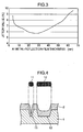
- FIG. 3 is a graphical representation, showing a measurement result of the jitter value which corresponds to the film thickness of the metal reflection film which is made of the Al alloy.
- the horizontal axis is the film thickness (nm) of the metal reflection film
- the vertical axis is the value (%) of a jitter.
- the material of a metal reflection film is not limited especially to those in the examples. Another material may also be used, as long as it has a high reflectance ratio and can be uniformly formed on a substrate by a film formation apparatus.
- a rare-earth metallic element such as Nd, or a transition metallic element such as Ti and Cr, may also be added a little to an Ag or Al reflection-film material.
- the quality of a reproduced signal will deteriorate when the quantity of reflected light decreases.
- the metal reflection film is made of a different material even though it has the same film thickness, that will change its reflectance ratio, and thereby, will change the film thickness at which the signal quality worsens.
- the metal reflection film becomes thicker, the reproduced signal will become worse.
- the metallic atoms on a target which have been sputtered by Ar ions come flying onto a substrate, so that a metal reflection film is formed.
- the size of these metallic atoms also depends upon the structure of a film formation apparatus, or the conditions of film formation. But such a film tends to be difficult to form at the bottom of the shortest pit.
- Fig. 4 is a sectional view of an optical disk in which a metal reflection film which is made of an AgPdCu alloy and has a film thickness of 100nm is formed on a substrate where pits are formed.
- a shortest pit 11 and a long pit 12 which is longer than the shortest pit 11 are formed on a substrate 1.
- a metal reflection film 2 is more difficult to form than at the bottom of the long pit 12. Therefore, the shortest pit 11 after the metal reflection film 2 has been formed becomes smaller, and at the same time, deeper than it was on the substrate 1.
- the maximum film thickness of the Al-alloy metal reflection film at which the value of a jitter was prevented from worsening was 40 nm
- the maximum film thickness of the AgPdCu-alloy metal reflection film at which it was prevented from worsening was 70 nm.
- a reflectance ratio was measured which corresponded to the film thickness of each of the AgPdCu-alloy metal reflection film which is shown in Fig. 2 and the Al-alloy metal reflection film which is shown in Fig. 3.
- Fig. 5 is a graphical representation, showing a measurement result of the reflectance ratio which corresponds to the film thickness of a metal reflection film which is made of an AgPdCu alloy.
- Fig. 6 is a graphical representation, showing a measurement result of the reflectance ratio which corresponds to the film thickness of a metal reflection film which is made of an Al alloy.
- the horizontal axis is the film thickness (nm) of the metal reflection film
- the vertical axis is the reflectance ratio (%).
- the refractive index n of the resin layer which was used for measurement is 1.53, and the wavelength ⁇ of the beam of light is 405nm.
- the reflectance ratio which corresponded to a film thickness of 25nm to 70nm at which a desirable jitter value was obtained was 35% to 70%.
- the reflectance ratio which corresponded to a film thickness of 15nm to 40nm at which a desirable jitter value was obtained was 35% to 70%.
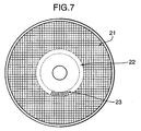
- Fig. 7 is a top view of an optical disk, showing an example of its main-information area and sub-information area.
- a main-information area 21 (which is a hatching part in the figure) is set in the outer circular part on the optical disk.
- a BCA area 22 (which is the area between two circles shown by broken lines in the figure) is set which is a sub-information area.
- medium identification information 23 is recorded in a bar-code pattern.
- a transparent resin layer of polycarbonate or the like is formed on the metal reflection film, and thereafter, the medium identification information 23 is recorded by irradiating, with a pulse laser (e.g., a YAG laser), the metal reflection film which lies at a depth of 0.1mm from the surface of the optical disk.
- a pulse laser e.g., a YAG laser
- the metal reflection film seems to melt, and then, accumulate at both boundary parts by surface tension. In this way, the metal reflection film is partially removed, and thus, several reflection-film removed areas are formed. This creates a BCA area where medium identification information is recorded which is used to identify the optical disk individually.
- the present invention can also be applied to other kinds of metal reflection films, a phase-change film, or an optical magnetic recording film.
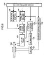
- Fig. 8 is a block diagram, showing the configuration of a medium-identification-information recording apparatus which records medium identification information in a BCA area.
- the medium-identification-information recording apparatus shown in Fig. 8 is a BCA-pattern recording apparatus which is used to create a BCA area in a DVD-ROM. It includes: a motor 101; a rotation control section 102; an optical pickup 103; a laser drive section 104; a waveform setting section 105; a BCA-signal generation section 106; a focus control section 107; a pre-amplifier 108; and a system control section 109.
- the rotation control section 102 controls the rotation of the motor 101.
- the motor 101 rotates an optical disk 100 at a predetermined rotational speed.
- the BCA-signal generation section 106 creates a BCA signal by modulating medium identification information which is recorded in the optical disk 100.
- the waveform setting section 105 creates a laser modulation waveform.
- the laser drive section 104 drives a high-power laser inside of the optical pickup 103.
- the optical pickup 103 converges a beam of light emitted from the high-power laser, through its built-in optical system, upon the optical disk 100.
- the pre-amplifier 108 amplifies a reproduced signal which comes from the optical pickup 103, and then, outputs it to the focus control section 107.
- the focus control section 107 controls an objective lens inside of the optical pickup 103, so that a beam of light can be converged on the metal reflection film of the optical disk 100.
- the system control section 109 systematically controls the operation of the rotation control section 102, the laser drive section 104, the waveform setting section 105, the BCA-signal generation section 106, and the focus control section 107.
- the rotation control section 102 drives the motor 101 to rotate the optical disk 100.
- the laser drive section 104 drives the high-power laser as a light source, and then, a beam of light which is emitted from the high-power laser is applied to the optical disk 100 from the optical pickup 103.
- the focus control section 107 executes focus control so that the beam of light which has been emitted from the high-power laser is converged on the metal reflection film of the optical disk 100.
- the reflected light from the optical disk 100 is detected by a photo-detector inside of the optical pickup 103. Then, a reproduced signal is outputted as an electric signal from the photo-detector. This reproduced signal is amplified through the pre-amplifier 108 and is inputted in the focus control section 107.
- the focus control section 107 drives the objective lens of the optical pickup 103 and moves it slightly in a focus direction on the optical disk 100. Thus, it controls the optical pickup 103 so that the beam of light can be converged on the metal reflection film of the optical disk 100.
- the system control section 109 allows a position detector (not shown) to detect the position of the optical pickup 103 in a tracking direction. Based on the detected positional information, it recognizes the optical pickup 103 to be located in a sub-information recording starting position.
- the system control section 109 instructs the BCA-signal generation section 106 to generate a BCA signal. Then, the BCA signal is outputted from the waveform setting section 105, a BCA recording sequence starts, and the medium identification information is recorded in the BCA area.
- the melting point of Al is 660°C while the melting point of Ag is 960°C. It takes a larger quantity of energy to melt the metal reflection film of an AgPdCu alloy.
- the thermal conductivity of Al is 237W/(m.K) while the thermal conductivity of Ag is 427°C. Therefore, a larger quantity of heat is diffused by the conduction of heat, even though the metal reflection film of an AgPdCu alloy is irradiated with a beam of light.
- the melting point of metal is lowered by mixing a different metal.
- the wt% of Ag in the metal reflection film cannot be reduced to 97% or below.
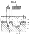
- Fig. 9 is a sectional view of an optical disk in which a metal reflection film is formed on a substrate where pits are formed, and in addition, a resin layer is formed on the metal reflection film.
- the metal reflection film 2 is formed on the substrate 1 where the pit 12 is formed, and in addition, a resin layer 3 is formed on the metal reflection film 2.
- the film thickness of the metal reflection film 2 which is formed on an inclined-surface part 4 becomes thinner than the film thickness of the metal reflection film 2 which is formed on each of a pit-bottom part 5 and a flat-plate part 6. Thereby, the quantity of heat which is conducted around becomes smaller.
- the volume per unit of the metal reflection film 2 is smaller than any other part. Therefore, its heat capacity necessary for reaching the melting point becomes smaller, and thus, it reaches the melting point with a lower irradiation power.
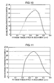
- Fig. 10 is a graphical representation, showing a measurement result of the defocus margin of a BCA recording power which corresponds to the track pitch of a row of pits which is formed in an optical disk that includes a 50nm metal reflection film which is made of an AgPdCu alloy. Its horizontal axis is the track pitch ( ⁇ m) of a row of pits and the vertical axis is the defocus margin (%).
- a BCA pattern could be recorded, and medium identification information could be recorded.
- the judgment that a BCA pattern was recorded was made by setting and reproducing the created optical disks in an assessment machine. It was made based upon whether or not the medium identification information which was recorded in the BCA area could be accurately reproduced.
- the assessment machine a reproducing apparatus was used in which a beam of light for reproduction had a wavelength ⁇ of 405 nm and an objective lens had a numerical aperture NA of 0.85.
- the track pitch at which a defocus margin of 20% or higher is obtained is 0.24 ⁇ m or wider and 0.45 ⁇ m or narrower.
- the track pitch of a row of pits which is recorded in the BCA area is 0.24 ⁇ m or wider and 0.45 ⁇ m or narrower, an adequate defocus margin can be secured, and medium identification information can be recorded. The presumable reason for this is described below.
- a pit is too close to its adjacent pits. Therefore, the formation of a land part between pits becomes inadequate, and the angle of the inclined-surface part of a pit becomes narrower. Thereby, a metal reflection film becomes easier to form on the inclined-surface parts of such pits, and thus, the effect of cutting off heat conduction by the formation of pits is reduced.
- a BCA pattern could be recorded and reproduced up to the point where the track pitch was 0.22 ⁇ m, while a BCA pattern could not be recorded when the track pitch was narrower than 0.22 ⁇ m.
- a dotted line is an estimated line which corresponds to a track pitch of 0.22 ⁇ m or below.
- Fig. 10 shows that in an optical disk where a 50nm-thick metal reflection film made of an AgPdCu alloy was formed, the defocus margin is dependent upon the track pitch.
- a metal reflection film which was made of Ag or an Ag alloy might also have a film thickness of 25nm or above and 70nm or below. In that case, if the track pitch of a row of pits which was recorded in a BCA area was 0.24 ⁇ m or wider and 0.45 ⁇ m or narrower, a defocus margin could be obtained at the same level as described above.
- a metal reflection film which was made of Ag or an Ag alloy had a film thickness of 25nm or above and 70nm or below, if the track pitch of a row of pits or a groove which was recorded in a BCA part was 0.24 ⁇ m or wider and 0.45 ⁇ m or narrower, then a defocus margin could be adequately secured.
- an optical disk whose metal reflection film was created by using a metal reflection film which was made of an Al99Cr1(wt%) (hereinafter, referred to as the Al reflection film).
- the Al reflection film having a film thickness of 30nm was formed.
- an attempt to record a BCA pattern was made in a part where neither a row of pits nor a groove was formed. In this case, a part could be formed in which the Al reflection film was removed, and in addition, the medium identification information which was recorded as the BCA pattern could also be reproduced.
- the Al reflection film was thinner than the one (i.e., 50 to 70nm) which was used in a DVD-ROM, and thus, an adequate defocus margin could not be obtained.
- the optical disk where the Al reflection film with a film thickness of 30nm was formed if a BCA pattern was recorded in the area where a row of pits was formed at the 0.74 ⁇ m track pitch which was used in the BCA area of the DVD-ROM, then the same result as described above was obtained.
- Fig. 11 is a graphical representation, showing a measurement result of the defocus margin of a BCA recording power which corresponds to the track pitch of a row of pits which is formed in an optical disk that includes an Al reflection film which has a film thickness of 30nm. Its horizontal axis is the track pitch ( ⁇ m) of a row of pits, and the vertical axis is the defocus margin (%).
- the track pitch at which a defocus margin of 20% or higher is obtained is 0.24 ⁇ m or wider and 0.45 ⁇ m or narrower.
- the edge part of a BCA pattern is not formed desirably, thus making louder the noise of a BCA reproduction signal.
- Fig. 11 shows that in an optical disk where a 30nm-thick metal reflection film made of an Al99Cr1(wt%) was formed, the defocus margin is dependent upon the track pitch.
- a metal reflection film which was made of Al or an Al alloy might also have a film thickness of 15nm or above and 40nm or below. In that case, if the track pitch of a row of pits which was recorded in a BCA area was 0.24 ⁇ m or wider and 0.45 ⁇ m or narrower, a defocus margin could be obtained at the same level as described above.
- a multi-layer optical disk which is a multi-layer optical recording medium which is formed by laminating a plurality of metal reflection films as information recording layers.
- a first metal reflection film which is made of Al and has a film thickness of 45nm is formed, using the above described magnetron sputtering apparatus.
- a second polycarbonate substrate having a thickness of 15 ⁇ m where pits are formed is glued, so that its side where those pits are not formed comes into contact.
- the adhesive for example, a resin to be hardened by light or the like is used which is strong in adhesive bonding.
- a metal reflection film which is made of AgPdCu and has a film thickness of 28nm.
- a transparent resin layer is glued which has a thickness of 70 ⁇ m.
- the adhesive for example, a pressure-sensitive adhesive sheet or the like is used.
- the method of creating a multi-layer optical disk is not limited especially to the above described example.
- a transparent resin layer Before a transparent resin layer is glued, a plurality of substrates may also be formed, so that a multi-layer optical disk can be obtained. In this case, even if an optical disk is layered, a focus is adjusted at the time of a BCA recording, and thereby, a BCA pattern can be recorded in a desired layer.
- a transparent resin layer and a polycarbonate substrate are glued, a light-hardened resin and a pressure-sensitive adhesive sheet are used. But instead of them, an adhesive and transparent medium, such as a dry photo-polymer, may also be used. Or, without gluing a transparent resin layer, a transparent resin layer may also be formed by using only a pressure-sensitive adhesive sheet, or only a light-hardened resin.
- the track pitch of a row of pits or a groove which was formed in the BCA area was set to 0.24 ⁇ m or wider and 0.45 ⁇ m or narrower.
- the track pitch of a row of pits or a groove in the BCA area is largely different from the track pitch of a row of pits in the main-information area
- the rotational speed of the disk has to be largely changed discontinuously.
- the main-information area is adjacent to the BCA area, and thus, the rotational speed of the disk needs to be controlled so that it becomes a desired rotational speed as fast as possible.
- the track pitch of a row of pits in the main-information area should be equal to the track pitch of a row of pits or a groove in the BCA area.
- the present invention using a beam of light for reproduction having a shorter wavelength and an optical system having a higher numerical aperture, data can be recorded at a higher density than in a DVD ROM optical disk.
- data can be recorded at a higher density than in a DVD ROM optical disk.
- medium identification information can be recorded so that an adequate defocus margin can be secured.
- the present invention can be suitably applied to an optical recording medium, for example, an optical disk which has a circular-plate shape and is used to generate information, or the like.
Landscapes
- Engineering & Computer Science (AREA)
- Manufacturing & Machinery (AREA)
- Optical Record Carriers And Manufacture Thereof (AREA)
- Optical Recording Or Reproduction (AREA)
- Manufacturing Optical Record Carriers (AREA)
Abstract
Description
| Track Pitch (µm) | Jitter Value (%) |
| 0.20 | 7.6 |
| 0.22 | 7.0 |
| 0.24 | 6.5 |
| 0.26 | 5.6 |
| 0.28 | 5.4 |
| Shortest-Pit Length (µm) | Jitter Value (%) |
| 0.10 | 8.2 |
| 0.11 | 6.8 |
| 0.12 | 6.5 |
| 0.13 | 5.4 |
| 0.14 | 5.3 |
Claims (20)
- An optical recording medium: which includes a main-information area in which a metal reflection film is formed on a substrate where a row of pits is formed as main data, and a sub-information area in which medium identification information is recorded which is used to identify the optical recording medium individually by removing the metal reflection film partially and forming a plurality of reflection-film removed areas; and in which information is reproduced by irradiating the metal reflection film with a beam of light, characterized in that,
in the sub-information area, a row of pits or a groove is formed on the substrate, and the track pitch of the row of pits or the groove is 0.24 µm or wider and 0.45 µm or narrower. - The optical recording medium according to claim 1, characterized in that the reflectance ratio of the metal reflection film is 35% or higher and 70% or lower, with respect to a beam of light whose wavelength is 405 nm.
- The optical recording medium according to claim 1, characterized in that the metal reflection film is made of Ag or an Ag alloy material, and the film thickness of the metal reflection film is 25nm or above and 70nm or below.
- The optical recording medium according to claim 1, characterized in that the metal reflection film is made of Al or an Al alloy material, and the film thickness of the metal reflection film is 15nm or above and 40nm or below.
- The optical recording medium according to claim 1, characterized in that if the wavelength of a light source of the beam of light is λ and the refractive index of a resin layer which is formed on the metal reflection film is n, the depth D of a row of pits or a groove which is formed on the substrate in the sub-information area satisfies a relational expression λ/(6×n)≦D≦λ/(3×n).
- The optical recording medium according to claim 1, characterized in that the depth of a row of pits which is formed on the substrate in the main-information area is equal to the depth of a row of pits or a groove which is formed on the substrate in the sub-information area.
- The optical recording medium according to claim 1, characterized in that the track pitch of a row of pits which is formed on the substrate in the main-information area is 0.24 µm or wider and 0.43 µm or narrower, and the shortest pit of a row of pits which is formed on the substrate in the main-information area is 0.12 µm or longer and 0.21 µm or shorter.
- The optical recording medium according to claim 1, characterized in that the track pitch of a row of pits which is formed on the substrate in the main-information area is equal to the track pitch of a row of pits or a groove which is formed on the substrate in the sub-information area.
- The optical recording medium according to claim 8, characterized in that the track pitch of a row of pits which is formed on the substrate in the main-information area and the track pitch of a row of pits or a groove which is formed on the substrate in the sub-information area are 0.24 µm or wider and 0.43 µm or narrower.
- The optical recording medium according to claim 1, characterized in that the optical recording medium is a multi-layer optical recording medium having a plurality of metal reflection films formed by laminating as the metal reflection film.
- Amanufacturingmethod for an optical recordingmedium, characterized by including:a first step of preparing a substrate on which a row of pits is formed as main data in a main-information area, and a row of pits or a groove whose track pitch is 0.24 µm or wider and 0.45 µm or narrower is formed in a sub-information area;a second step of forming a metal reflection film on the substrate;a third step of forming a resin layer on the metal reflection film; anda fourth step of recording medium identification information which is used to identify the optical recording medium individually by partially removing the metal reflection film in the sub-information area and forming a plurality of reflection-film removed areas.
- The manufacturing method for an optical recording medium according to claim 11, characterized in that the second step has a step of forming a metal reflection film which has a reflectance ratio of 35% or higher and 70% or lower with respect to a beam of light whose wavelength is 405nm.
- The manufacturing method for an optical recording medium according to claim 11, characterized in that the second step has a step of forming a metal reflection film which is made of Ag or an Ag alloy material, so that the film thickness thereof is 25nm or above and 70nm or below.
- The manufacturing method for an optical recording medium according to claim 11, characterized in that the second step has a step of forming a metal reflection film which is made of Al or an Al alloy material, so that the film thickness thereof is 15nm or above and 40nm or below.
- The manufacturing method for an optical recording medium according to claim 11, characterized in that the first step has a step of forming a row of pits or a groove on the substrate in the sub-information area, so that if the wavelength of a light source of the beam of light is λ and the refractive index of the resin layer which is formed on the metal reflection film is n, the depth D of the row of pits or the groove formed on the substrate in the sub-information area satisfies a relational expression λ/(6×n)≦D≦λ/(3×n).
- The manufacturing method for an optical recording medium according to claim 11, characterized in that the first step has a step of forming a row of pits on the substrate in the main-information area and forming a row of pits or a groove on the substrate in the sub-information area, so that the depth of the row of pits formed on the substrate in the main-information area is equal to the depth of the row of pits or the groove formed on the substrate in the sub-information area.
- The manufacturing method for an optical recording medium according to claim 11, characterized in that the first step has a step of forming a row of pits on the substrate in the main-information area, so that the track pitch of the row of pits formed on the substrate in the main-information area is 0.24 µm or wider and 0.43 µm or narrower, and the shortest pit of the row of pits formed on the substrate in the main-information area is 0.12 µm or longer and 0.21 µm or shorter.
- The manufacturing method for an optical recording medium according to claim 11, characterized in that the first step has a step of forming a row of pits on the substrate in the main-information area and forming a row of pits or a groove on the substrate in the sub-information area, so that the track pitch of the row of pits formed on the substrate in the main-information area is equal to the track pitch of the row of pits or the groove formed on the substrate in the sub-information area.
- The manufacturing method for an optical recording medium according to claim 11, characterized in that the first step has a step of simultaneously forming a row of pits in the main-information area and a row of pits or a groove in the sub-information area.
- A reproducing method for an optical recording medium, characterized in that: the optical recording medium includes a main-information area in which a metal reflection film is formed on a substrate where a row of pits is formed as main data, and a sub-information area in which a row of pits or a groove whose track pitch is 0.24 µm or wider and 0.45 µm or narrower is formed on the substrate, and medium identification information is recorded which is used to identify the optical recording medium individually by removing the metal reflection film partially and forming a plurality of reflection-film removed areas; and information is reproduced by irradiating the metal reflection film of the optical recording medium with a beam of light.
Priority Applications (7)
| Application Number | Priority Date | Filing Date | Title |
|---|---|---|---|
| PL09170807T PL2146347T3 (en) | 2003-04-14 | 2004-03-16 | Manufacturing method for optical recording medium |
| EP10165980A EP2242050B1 (en) | 2003-04-14 | 2004-03-16 | Optical recording medium |
| PL10165983T PL2244257T3 (en) | 2003-04-14 | 2004-03-16 | Optical recording medium |
| PL04720984T PL1524652T3 (en) | 2003-04-14 | 2004-03-16 | Optical recording medium and optical recording medium reproducing method |
| PL10165980T PL2242050T3 (en) | 2003-04-14 | 2004-03-16 | Optical recording medium |
| EP09170807A EP2146347B1 (en) | 2003-04-14 | 2004-03-16 | Manufacturing method for optical recording medium |
| EP10165983A EP2244257B1 (en) | 2003-04-14 | 2004-03-16 | Optical recording medium |
Applications Claiming Priority (3)
| Application Number | Priority Date | Filing Date | Title |
|---|---|---|---|
| JP2003108549 | 2003-04-14 | ||
| JP2003108549A JP4170132B2 (en) | 2003-04-14 | 2003-04-14 | Optical recording medium |
| PCT/JP2004/003459 WO2004093066A1 (en) | 2003-04-14 | 2004-03-16 | Optical recording medium, optical recording medium manufacturing method, and optical recording medium reproducing method |
Related Child Applications (1)
| Application Number | Title | Priority Date | Filing Date |
|---|---|---|---|
| EP09170807A Division EP2146347B1 (en) | 2003-04-14 | 2004-03-16 | Manufacturing method for optical recording medium |
Publications (3)
| Publication Number | Publication Date |
|---|---|
| EP1524652A1 true EP1524652A1 (en) | 2005-04-20 |
| EP1524652A4 EP1524652A4 (en) | 2009-01-14 |
| EP1524652B1 EP1524652B1 (en) | 2010-01-06 |
Family
ID=33156936
Family Applications (4)
| Application Number | Title | Priority Date | Filing Date |
|---|---|---|---|
| EP04720984A Expired - Lifetime EP1524652B1 (en) | 2003-04-14 | 2004-03-16 | Optical recording medium and optical recording medium reproducing method |
| EP09170807A Expired - Lifetime EP2146347B1 (en) | 2003-04-14 | 2004-03-16 | Manufacturing method for optical recording medium |
| EP10165983A Expired - Lifetime EP2244257B1 (en) | 2003-04-14 | 2004-03-16 | Optical recording medium |
| EP10165980A Expired - Lifetime EP2242050B1 (en) | 2003-04-14 | 2004-03-16 | Optical recording medium |
Family Applications After (3)
| Application Number | Title | Priority Date | Filing Date |
|---|---|---|---|
| EP09170807A Expired - Lifetime EP2146347B1 (en) | 2003-04-14 | 2004-03-16 | Manufacturing method for optical recording medium |
| EP10165983A Expired - Lifetime EP2244257B1 (en) | 2003-04-14 | 2004-03-16 | Optical recording medium |
| EP10165980A Expired - Lifetime EP2242050B1 (en) | 2003-04-14 | 2004-03-16 | Optical recording medium |
Country Status (15)
| Country | Link |
|---|---|
| US (4) | US7808881B2 (en) |
| EP (4) | EP1524652B1 (en) |
| JP (1) | JP4170132B2 (en) |
| KR (1) | KR100674302B1 (en) |
| CN (1) | CN1698099A (en) |
| AT (4) | ATE528756T1 (en) |
| AU (1) | AU2004214550B2 (en) |
| BR (1) | BRPI0403931A (en) |
| CA (1) | CA2477869A1 (en) |
| DE (1) | DE602004024946D1 (en) |
| ES (4) | ES2370701T3 (en) |
| MX (1) | MXPA04011159A (en) |
| PL (4) | PL2146347T3 (en) |
| RU (1) | RU2279723C2 (en) |
| WO (1) | WO2004093066A1 (en) |
Cited By (3)
| Publication number | Priority date | Publication date | Assignee | Title |
|---|---|---|---|---|
| EP1662495A3 (en) * | 2004-11-30 | 2006-11-29 | Kabushiki Kaisha Toshiba | Information Storage Medium |
| EP1742212A1 (en) * | 2005-06-27 | 2007-01-10 | Nec Corporation | Optical information recording medium and optical information reproducing apparatus |
| EP2146347A1 (en) | 2003-04-14 | 2010-01-20 | Panasonic Corporation | Manufacturing method for optical recording medium |
Families Citing this family (12)
| Publication number | Priority date | Publication date | Assignee | Title |
|---|---|---|---|---|
| DE60321321D1 (en) * | 2002-02-18 | 2008-07-10 | Matsushita Electric Industrial Co Ltd | EVER DRIVE |
| KR20050042804A (en) * | 2002-09-13 | 2005-05-10 | 마츠시타 덴끼 산교 가부시키가이샤 | Optical recording medium and method for producing the same |
| JP2006155785A (en) * | 2004-11-30 | 2006-06-15 | Toshiba Corp | Information storage medium, stamper, disk device, and management information reproducing method |
| JP2007102984A (en) * | 2005-10-07 | 2007-04-19 | Pioneer Electronic Corp | Optical disk |
| RU2411193C2 (en) * | 2006-06-15 | 2011-02-10 | Александр Михайлович Ефимов | Method of purifying mine water from iron |
| JP4262730B2 (en) * | 2006-06-15 | 2009-05-13 | ソニー株式会社 | Optical recording medium having a metal reflective film capable of additional recording |
| JP2008004151A (en) * | 2006-06-21 | 2008-01-10 | Toshiba Corp | Single-sided multilayer optical disk, BCA recording apparatus, BCA recording method, and optical disk apparatus |
| JP2008159203A (en) * | 2006-12-26 | 2008-07-10 | Tdk Corp | Optical recording medium, and recording and reproducing method of optical recording medium |
| JP4839262B2 (en) * | 2007-05-17 | 2011-12-21 | 株式会社日立製作所 | Multi-layer optical disc |
| CN102272836A (en) * | 2009-02-27 | 2011-12-07 | 三菱电机株式会社 | BCA recording device for optical disc, optical disc reproducing device, and recordable optical disc |
| AU2010268091B2 (en) * | 2009-06-30 | 2015-01-29 | Sanofi-Aventis Deutschland Gmbh | Circular bar-code for drug container |
| CN102326199B (en) * | 2009-12-22 | 2014-11-05 | 松下电器产业株式会社 | Optical disc device, optical disc control method, and integrated circuit |
Family Cites Families (42)
| Publication number | Priority date | Publication date | Assignee | Title |
|---|---|---|---|---|
| US5013594A (en) * | 1987-09-25 | 1991-05-07 | Hitachi Maxwell, Ltd. | Optical information recording medium and its production |
| US5016240A (en) * | 1987-10-07 | 1991-05-14 | The Dow Chemical Company | Optical recording medium |
| EP0348122B1 (en) * | 1988-06-20 | 1999-12-08 | Hitachi Maxell Ltd. | Optical data recording medium and manufacturing method thereof |
| JPH0255347A (en) * | 1988-08-19 | 1990-02-23 | Brother Ind Ltd | image forming device |
| JP2995822B2 (en) | 1990-08-23 | 1999-12-27 | ソニー株式会社 | Recording device and reproducing device for disk-shaped recording medium |
| JP2973155B2 (en) * | 1993-10-29 | 1999-11-08 | 株式会社名機製作所 | Disk substrate and molding die used for molding the disk substrate |
| JPH0816401A (en) | 1994-06-30 | 1996-01-19 | Toyota Motor Corp | Node inference method and production schedule planning method using the same |
| DE69535603T2 (en) * | 1994-11-17 | 2008-02-21 | Matsushita Electric Industrial Co., Ltd., Kadoma | Optical disc, method of manufacturing an optical disc and reproducing apparatus |
| JP3786015B2 (en) | 1995-10-09 | 2006-06-14 | 松下電器産業株式会社 | Encryption recording apparatus and encryption recording method |
| JPH10233019A (en) | 1996-01-22 | 1998-09-02 | Matsushita Electric Ind Co Ltd | Optical disk, optical disk manufacturing device, optical disk reproducing device |
| EP1271490B1 (en) | 1996-10-23 | 2011-12-21 | Panasonic Corporation | Optical disk |
| JP3209126B2 (en) * | 1996-12-20 | 2001-09-17 | 日本ビクター株式会社 | Optical recording medium, optical disk reproducing apparatus, and optical disk reproducing method |
| JPH10255269A (en) | 1997-01-10 | 1998-09-25 | Sony Corp | Optical disc reproducing method and optical disc reproducing apparatus |
| JP2000011453A (en) * | 1998-06-29 | 2000-01-14 | Sony Corp | Optical recording medium and optical recording / reproducing device |
| US6175548B1 (en) | 1998-06-29 | 2001-01-16 | Sony Corporation | Optical recording medium and optical recording and reproducing apparatus |
| JP3524772B2 (en) | 1998-08-11 | 2004-05-10 | メモリーテック株式会社 | Laminated disk and method of checking the configuration disk of the laminated disk |
| JP2001006210A (en) * | 1999-06-22 | 2001-01-12 | Sony Corp | Optical recording medium and disk cartridge |
| EP1152402B1 (en) | 1999-07-15 | 2006-11-15 | Matsushita Electric Industrial Co., Ltd. | Optical recording medium and method for recording optical recording medium |
| JP3224380B2 (en) * | 1999-07-15 | 2001-10-29 | 松下電器産業株式会社 | Optical recording medium recording method |
| JP2001084643A (en) | 1999-09-09 | 2001-03-30 | Hitachi Ltd | Optical disk media |
| US6708299B1 (en) * | 1999-11-22 | 2004-03-16 | Thomson Licensing S.A. | BCA data replay |
| JP3880759B2 (en) * | 1999-12-20 | 2007-02-14 | 富士通株式会社 | Moving object detection method |
| US20010015949A1 (en) * | 1999-12-28 | 2001-08-23 | Toshihiko Nagase | Optical recording medium and recording-reproducing apparatus |
| JP2001202659A (en) | 2000-01-20 | 2001-07-27 | Victor Co Of Japan Ltd | Recording type optical disk and method of manufacturing the same |
| JP2001216686A (en) * | 2000-01-31 | 2001-08-10 | Sony Corp | Optical recording medium |
| JP2002230834A (en) * | 2000-06-26 | 2002-08-16 | Tdk Corp | Optical information medium, method of manufacturing for the same, recording or reproducing method for the same and method of inspecting the same |
| US6808778B2 (en) * | 2000-07-04 | 2004-10-26 | Tdk Corporation | Optical recording medium |
| JP2002237102A (en) * | 2000-07-07 | 2002-08-23 | Tdk Corp | Optical recording medium and manufacturing method thereof |
| AU2002214264A1 (en) * | 2000-11-06 | 2002-05-15 | Matsushita Electric Industrial Co., Ltd. | Optical recording medium, optical recording medium production method, optical recording medium production apparatus, program, and medium |
| DE60137714D1 (en) * | 2000-12-28 | 2009-04-02 | Sony Corp | OPTICAL RECORDING MEDIUM |
| CN1248201C (en) * | 2001-10-02 | 2006-03-29 | 松下电器产业株式会社 | optical information recording method, regenerater and medium |
| WO2003065358A2 (en) * | 2002-01-28 | 2003-08-07 | Burstein Technologies, Inc. | Methods and apparatus for logical triggering of an optical bio-disc |
| DE60321321D1 (en) | 2002-02-18 | 2008-07-10 | Matsushita Electric Industrial Co Ltd | EVER DRIVE |
| JP2003281780A (en) * | 2002-03-26 | 2003-10-03 | Toshiba Corp | Optical recording medium |
| JP2004005872A (en) * | 2002-04-09 | 2004-01-08 | Matsushita Electric Ind Co Ltd | Method for manufacturing optical disk master, optical disk and method for manufacturing the same |
| US7177262B2 (en) * | 2002-04-19 | 2007-02-13 | Victor Company Of Japan, Ltd. | Reproducing system and corresponding information recording medium having wobbled land portions |
| JP2004014088A (en) * | 2002-06-11 | 2004-01-15 | Sony Corp | Disk recording medium, recording method, disk drive device |
| ATE441181T1 (en) * | 2002-10-18 | 2009-09-15 | Panasonic Corp | INFORMATION RECORDING MEDIUM, INFORMATION RECORDING DEVICE AND INFORMATION REPRODUCTION DEVICE THEREFOR |
| KR20040069750A (en) * | 2003-01-30 | 2004-08-06 | 삼성전자주식회사 | Optical information storage medium |
| KR100727919B1 (en) * | 2003-02-03 | 2007-06-14 | 삼성전자주식회사 | Optical information storage medium |
| JP4170132B2 (en) | 2003-04-14 | 2008-10-22 | 松下電器産業株式会社 | Optical recording medium |
| TW200634801A (en) * | 2004-11-17 | 2006-10-01 | Hitachi Maxell | Optical information-recording medium |
-
2003
- 2003-04-14 JP JP2003108549A patent/JP4170132B2/en not_active Expired - Fee Related
-
2004
- 2004-03-16 AT AT10165980T patent/ATE528756T1/en active
- 2004-03-16 KR KR1020047013676A patent/KR100674302B1/en not_active Expired - Fee Related
- 2004-03-16 CA CA002477869A patent/CA2477869A1/en not_active Abandoned
- 2004-03-16 PL PL09170807T patent/PL2146347T3/en unknown
- 2004-03-16 BR BR0403931-9A patent/BRPI0403931A/en not_active Application Discontinuation
- 2004-03-16 MX MXPA04011159A patent/MXPA04011159A/en active IP Right Grant
- 2004-03-16 ES ES10165980T patent/ES2370701T3/en not_active Expired - Lifetime
- 2004-03-16 EP EP04720984A patent/EP1524652B1/en not_active Expired - Lifetime
- 2004-03-16 AT AT10165983T patent/ATE525723T1/en active
- 2004-03-16 DE DE602004024946T patent/DE602004024946D1/en not_active Expired - Lifetime
- 2004-03-16 US US10/509,745 patent/US7808881B2/en not_active Expired - Lifetime
- 2004-03-16 EP EP09170807A patent/EP2146347B1/en not_active Expired - Lifetime
- 2004-03-16 WO PCT/JP2004/003459 patent/WO2004093066A1/en not_active Ceased
- 2004-03-16 AT AT04720984T patent/ATE454699T1/en active
- 2004-03-16 ES ES10165983T patent/ES2369878T3/en not_active Expired - Lifetime
- 2004-03-16 EP EP10165983A patent/EP2244257B1/en not_active Expired - Lifetime
- 2004-03-16 EP EP10165980A patent/EP2242050B1/en not_active Expired - Lifetime
- 2004-03-16 AU AU2004214550A patent/AU2004214550B2/en not_active Ceased
- 2004-03-16 PL PL04720984T patent/PL1524652T3/en unknown
- 2004-03-16 ES ES04720984T patent/ES2339019T3/en not_active Expired - Lifetime
- 2004-03-16 RU RU2004133023/28A patent/RU2279723C2/en not_active IP Right Cessation
- 2004-03-16 CN CNA200480000067XA patent/CN1698099A/en active Pending
- 2004-03-16 AT AT09170807T patent/ATE515024T1/en active
- 2004-03-16 PL PL10165980T patent/PL2242050T3/en unknown
- 2004-03-16 ES ES09170807T patent/ES2366428T3/en not_active Expired - Lifetime
- 2004-03-16 PL PL10165983T patent/PL2244257T3/en unknown
-
2008
- 2008-08-19 US US12/194,276 patent/US8116193B2/en not_active Expired - Fee Related
- 2008-09-25 US US12/237,613 patent/US7821909B2/en not_active Expired - Fee Related
-
2010
- 2010-08-31 US US12/872,214 patent/US7948860B2/en not_active Expired - Fee Related
Cited By (3)
| Publication number | Priority date | Publication date | Assignee | Title |
|---|---|---|---|---|
| EP2146347A1 (en) | 2003-04-14 | 2010-01-20 | Panasonic Corporation | Manufacturing method for optical recording medium |
| EP1662495A3 (en) * | 2004-11-30 | 2006-11-29 | Kabushiki Kaisha Toshiba | Information Storage Medium |
| EP1742212A1 (en) * | 2005-06-27 | 2007-01-10 | Nec Corporation | Optical information recording medium and optical information reproducing apparatus |
Also Published As
Similar Documents
| Publication | Publication Date | Title |
|---|---|---|
| US7948860B2 (en) | Optical recording medium, manufacturing method for optical recording medium, and reproducing method for optical recording medium | |
| CN100399427C (en) | Optical disk, its manufacturing method, and recording and reproducing device | |
| WO2001018802A1 (en) | Rewritable compact disk and method for manufacturing the same | |
| JP4349248B2 (en) | Optical information recording medium, reproducing method thereof and manufacturing method thereof | |
| JP4161716B2 (en) | Optical recording medium and optical disc apparatus | |
| JP4193408B2 (en) | Optical recording medium and method for manufacturing the same, optical recording method, and optical reproducing method | |
| CN101393755A (en) | Optical information reproducing method, optical information reproducing device, and optical information recording medium | |
| JP4539664B2 (en) | Information playback method | |
| JP4659870B2 (en) | Optical recording medium | |
| JP4238284B2 (en) | Optical recording medium | |
| JP4199301B2 (en) | Optical recording medium | |
| JP4235249B2 (en) | Optical recording medium | |
| JP4217270B1 (en) | Optical recording medium | |
| JP4217269B2 (en) | Optical recording medium | |
| JP2011048901A (en) | Optical recording medium | |
| JPWO2001016947A1 (en) | Optical disc, playback method for playing back data from this optical disc, and playback device | |
| WO2005024810A1 (en) | Information recording medium |
Legal Events
| Date | Code | Title | Description |
|---|---|---|---|
| PUAI | Public reference made under article 153(3) epc to a published international application that has entered the european phase |
Free format text: ORIGINAL CODE: 0009012 |
|
| 17P | Request for examination filed |
Effective date: 20040921 |
|
| AK | Designated contracting states |
Kind code of ref document: A1 Designated state(s): AT BE BG CH CY CZ DE DK EE ES FI FR GB GR HU IE IT LI LU MC NL PL PT RO SE SI SK TR |
|
| AX | Request for extension of the european patent |
Extension state: AL LT LV MK |
|
| DAX | Request for extension of the european patent (deleted) | ||
| RAP1 | Party data changed (applicant data changed or rights of an application transferred) |
Owner name: PANASONIC CORPORATION |
|
| A4 | Supplementary search report drawn up and despatched |
Effective date: 20081212 |
|
| RIC1 | Information provided on ipc code assigned before grant |
Ipc: G11B 7/26 20060101ALI20081208BHEP Ipc: G11B 7/007 20060101AFI20081208BHEP |
|
| 17Q | First examination report despatched |
Effective date: 20090319 |
|
| GRAP | Despatch of communication of intention to grant a patent |
Free format text: ORIGINAL CODE: EPIDOSNIGR1 |
|
| GRAS | Grant fee paid |
Free format text: ORIGINAL CODE: EPIDOSNIGR3 |
|
| GRAA | (expected) grant |
Free format text: ORIGINAL CODE: 0009210 |
|
| AK | Designated contracting states |
Kind code of ref document: B1 Designated state(s): AT BE BG CH CY CZ DE DK EE ES FI FR GB GR HU IE IT LI LU MC NL PL PT RO SE SI SK TR |
|
| REG | Reference to a national code |
Ref country code: GB Ref legal event code: FG4D |
|
| REG | Reference to a national code |
Ref country code: CH Ref legal event code: EP |
|
| REG | Reference to a national code |
Ref country code: IE Ref legal event code: FG4D |
|
| REF | Corresponds to: |
Ref document number: 602004024946 Country of ref document: DE Date of ref document: 20100225 Kind code of ref document: P |
|
| REG | Reference to a national code |
Ref country code: NL Ref legal event code: VDEP Effective date: 20100106 |
|
| REG | Reference to a national code |
Ref country code: ES Ref legal event code: FG2A Ref document number: 2339019 Country of ref document: ES Kind code of ref document: T3 |
|
| PG25 | Lapsed in a contracting state [announced via postgrant information from national office to epo] |
Ref country code: SI Free format text: LAPSE BECAUSE OF FAILURE TO SUBMIT A TRANSLATION OF THE DESCRIPTION OR TO PAY THE FEE WITHIN THE PRESCRIBED TIME-LIMIT Effective date: 20100106 |
|
| PG25 | Lapsed in a contracting state [announced via postgrant information from national office to epo] |
Ref country code: NL Free format text: LAPSE BECAUSE OF FAILURE TO SUBMIT A TRANSLATION OF THE DESCRIPTION OR TO PAY THE FEE WITHIN THE PRESCRIBED TIME-LIMIT Effective date: 20100106 Ref country code: PT Free format text: LAPSE BECAUSE OF FAILURE TO SUBMIT A TRANSLATION OF THE DESCRIPTION OR TO PAY THE FEE WITHIN THE PRESCRIBED TIME-LIMIT Effective date: 20100506 |
|
| PG25 | Lapsed in a contracting state [announced via postgrant information from national office to epo] |
Ref country code: FI Free format text: LAPSE BECAUSE OF FAILURE TO SUBMIT A TRANSLATION OF THE DESCRIPTION OR TO PAY THE FEE WITHIN THE PRESCRIBED TIME-LIMIT Effective date: 20100106 |
|
| PG25 | Lapsed in a contracting state [announced via postgrant information from national office to epo] |
Ref country code: GR Free format text: LAPSE BECAUSE OF FAILURE TO SUBMIT A TRANSLATION OF THE DESCRIPTION OR TO PAY THE FEE WITHIN THE PRESCRIBED TIME-LIMIT Effective date: 20100407 Ref country code: CY Free format text: LAPSE BECAUSE OF FAILURE TO SUBMIT A TRANSLATION OF THE DESCRIPTION OR TO PAY THE FEE WITHIN THE PRESCRIBED TIME-LIMIT Effective date: 20100106 Ref country code: BE Free format text: LAPSE BECAUSE OF FAILURE TO SUBMIT A TRANSLATION OF THE DESCRIPTION OR TO PAY THE FEE WITHIN THE PRESCRIBED TIME-LIMIT Effective date: 20100106 Ref country code: SE Free format text: LAPSE BECAUSE OF FAILURE TO SUBMIT A TRANSLATION OF THE DESCRIPTION OR TO PAY THE FEE WITHIN THE PRESCRIBED TIME-LIMIT Effective date: 20100106 Ref country code: RO Free format text: LAPSE BECAUSE OF FAILURE TO SUBMIT A TRANSLATION OF THE DESCRIPTION OR TO PAY THE FEE WITHIN THE PRESCRIBED TIME-LIMIT Effective date: 20100106 Ref country code: MC Free format text: LAPSE BECAUSE OF NON-PAYMENT OF DUE FEES Effective date: 20100331 Ref country code: EE Free format text: LAPSE BECAUSE OF FAILURE TO SUBMIT A TRANSLATION OF THE DESCRIPTION OR TO PAY THE FEE WITHIN THE PRESCRIBED TIME-LIMIT Effective date: 20100106 |
|
| REG | Reference to a national code |
Ref country code: CH Ref legal event code: PL |
|
| PLBE | No opposition filed within time limit |
Free format text: ORIGINAL CODE: 0009261 |
|
| STAA | Information on the status of an ep patent application or granted ep patent |
Free format text: STATUS: NO OPPOSITION FILED WITHIN TIME LIMIT |
|
| PG25 | Lapsed in a contracting state [announced via postgrant information from national office to epo] |
Ref country code: CZ Free format text: LAPSE BECAUSE OF FAILURE TO SUBMIT A TRANSLATION OF THE DESCRIPTION OR TO PAY THE FEE WITHIN THE PRESCRIBED TIME-LIMIT Effective date: 20100106 Ref country code: SK Free format text: LAPSE BECAUSE OF FAILURE TO SUBMIT A TRANSLATION OF THE DESCRIPTION OR TO PAY THE FEE WITHIN THE PRESCRIBED TIME-LIMIT Effective date: 20100106 |
|
| 26N | No opposition filed |
Effective date: 20101007 |
|
| PG25 | Lapsed in a contracting state [announced via postgrant information from national office to epo] |
Ref country code: IE Free format text: LAPSE BECAUSE OF NON-PAYMENT OF DUE FEES Effective date: 20100316 Ref country code: DK Free format text: LAPSE BECAUSE OF FAILURE TO SUBMIT A TRANSLATION OF THE DESCRIPTION OR TO PAY THE FEE WITHIN THE PRESCRIBED TIME-LIMIT Effective date: 20100106 |
|
| PG25 | Lapsed in a contracting state [announced via postgrant information from national office to epo] |
Ref country code: LI Free format text: LAPSE BECAUSE OF NON-PAYMENT OF DUE FEES Effective date: 20100331 Ref country code: CH Free format text: LAPSE BECAUSE OF NON-PAYMENT OF DUE FEES Effective date: 20100331 |
|
| PG25 | Lapsed in a contracting state [announced via postgrant information from national office to epo] |
Ref country code: HU Free format text: LAPSE BECAUSE OF FAILURE TO SUBMIT A TRANSLATION OF THE DESCRIPTION OR TO PAY THE FEE WITHIN THE PRESCRIBED TIME-LIMIT Effective date: 20100707 Ref country code: LU Free format text: LAPSE BECAUSE OF NON-PAYMENT OF DUE FEES Effective date: 20100316 |
|
| REG | Reference to a national code |
Ref country code: FR Ref legal event code: PLFP Year of fee payment: 13 |
|
| REG | Reference to a national code |
Ref country code: FR Ref legal event code: PLFP Year of fee payment: 14 |
|
| REG | Reference to a national code |
Ref country code: FR Ref legal event code: PLFP Year of fee payment: 15 |
|
| PGFP | Annual fee paid to national office [announced via postgrant information from national office to epo] |
Ref country code: GB Payment date: 20190313 Year of fee payment: 16 Ref country code: BG Payment date: 20190226 Year of fee payment: 16 Ref country code: PL Payment date: 20190129 Year of fee payment: 16 Ref country code: DE Payment date: 20190305 Year of fee payment: 16 Ref country code: IT Payment date: 20190326 Year of fee payment: 16 |
|
| PGFP | Annual fee paid to national office [announced via postgrant information from national office to epo] |
Ref country code: FR Payment date: 20190213 Year of fee payment: 16 Ref country code: TR Payment date: 20190311 Year of fee payment: 16 Ref country code: AT Payment date: 20190226 Year of fee payment: 16 |
|
| PGFP | Annual fee paid to national office [announced via postgrant information from national office to epo] |
Ref country code: ES Payment date: 20190402 Year of fee payment: 16 |
|
| REG | Reference to a national code |
Ref country code: DE Ref legal event code: R119 Ref document number: 602004024946 Country of ref document: DE |
|
| REG | Reference to a national code |
Ref country code: AT Ref legal event code: MM01 Ref document number: 454699 Country of ref document: AT Kind code of ref document: T Effective date: 20200316 |
|
| PG25 | Lapsed in a contracting state [announced via postgrant information from national office to epo] |
Ref country code: DE Free format text: LAPSE BECAUSE OF NON-PAYMENT OF DUE FEES Effective date: 20201001 Ref country code: AT Free format text: LAPSE BECAUSE OF NON-PAYMENT OF DUE FEES Effective date: 20200316 Ref country code: FR Free format text: LAPSE BECAUSE OF NON-PAYMENT OF DUE FEES Effective date: 20200331 Ref country code: BG Free format text: LAPSE BECAUSE OF NON-PAYMENT OF DUE FEES Effective date: 20201130 |
|
| GBPC | Gb: european patent ceased through non-payment of renewal fee |
Effective date: 20200316 |
|
| PG25 | Lapsed in a contracting state [announced via postgrant information from national office to epo] |
Ref country code: GB Free format text: LAPSE BECAUSE OF NON-PAYMENT OF DUE FEES Effective date: 20200316 |
|
| REG | Reference to a national code |
Ref country code: ES Ref legal event code: FD2A Effective date: 20210730 |
|
| PG25 | Lapsed in a contracting state [announced via postgrant information from national office to epo] |
Ref country code: IT Free format text: LAPSE BECAUSE OF NON-PAYMENT OF DUE FEES Effective date: 20200316 |
|
| PG25 | Lapsed in a contracting state [announced via postgrant information from national office to epo] |
Ref country code: ES Free format text: LAPSE BECAUSE OF NON-PAYMENT OF DUE FEES Effective date: 20200317 |
|
| PG25 | Lapsed in a contracting state [announced via postgrant information from national office to epo] |
Ref country code: TR Free format text: LAPSE BECAUSE OF NON-PAYMENT OF DUE FEES Effective date: 20200316 |
|
| PG25 | Lapsed in a contracting state [announced via postgrant information from national office to epo] |
Ref country code: PL Free format text: LAPSE BECAUSE OF NON-PAYMENT OF DUE FEES Effective date: 20200316 |