EP1524556A1 - Lithographic apparatus, device manufacturing method and positioning system - Google Patents
Lithographic apparatus, device manufacturing method and positioning system Download PDFInfo
- Publication number
- EP1524556A1 EP1524556A1 EP03078282A EP03078282A EP1524556A1 EP 1524556 A1 EP1524556 A1 EP 1524556A1 EP 03078282 A EP03078282 A EP 03078282A EP 03078282 A EP03078282 A EP 03078282A EP 1524556 A1 EP1524556 A1 EP 1524556A1
- Authority
- EP
- European Patent Office
- Prior art keywords
- actuators
- actuator
- lithographic apparatus
- elements
- shield
- Prior art date
- Legal status (The legal status is an assumption and is not a legal conclusion. Google has not performed a legal analysis and makes no representation as to the accuracy of the status listed.)
- Withdrawn
Links
- 238000004519 manufacturing process Methods 0.000 title claims description 7
- 239000000758 substrate Substances 0.000 claims description 43
- 230000005855 radiation Effects 0.000 claims description 23
- 238000000059 patterning Methods 0.000 claims description 21
- 230000005291 magnetic effect Effects 0.000 claims description 14
- 238000005286 illumination Methods 0.000 claims description 9
- 239000000463 material Substances 0.000 claims description 8
- 230000035699 permeability Effects 0.000 claims description 6
- 229910000831 Steel Inorganic materials 0.000 claims description 4
- 239000010959 steel Substances 0.000 claims description 4
- 239000003302 ferromagnetic material Substances 0.000 claims description 3
- 239000000919 ceramic Substances 0.000 claims description 2
- 239000011248 coating agent Substances 0.000 claims description 2
- 238000000576 coating method Methods 0.000 claims description 2
- 229910052751 metal Inorganic materials 0.000 claims description 2
- 239000002184 metal Substances 0.000 claims description 2
- 230000000694 effects Effects 0.000 description 6
- 230000003287 optical effect Effects 0.000 description 6
- 239000010410 layer Substances 0.000 description 5
- 238000009826 distribution Methods 0.000 description 3
- 230000005484 gravity Effects 0.000 description 3
- 238000007654 immersion Methods 0.000 description 3
- 230000003467 diminishing effect Effects 0.000 description 2
- 230000005672 electromagnetic field Effects 0.000 description 2
- 239000007788 liquid Substances 0.000 description 2
- 238000001459 lithography Methods 0.000 description 2
- 230000010363 phase shift Effects 0.000 description 2
- 230000003068 static effect Effects 0.000 description 2
- XUIMIQQOPSSXEZ-UHFFFAOYSA-N Silicon Chemical compound [Si] XUIMIQQOPSSXEZ-UHFFFAOYSA-N 0.000 description 1
- 230000001133 acceleration Effects 0.000 description 1
- 238000003491 array Methods 0.000 description 1
- 230000002238 attenuated effect Effects 0.000 description 1
- 230000001143 conditioned effect Effects 0.000 description 1
- 238000010276 construction Methods 0.000 description 1
- 238000001514 detection method Methods 0.000 description 1
- 230000009977 dual effect Effects 0.000 description 1
- 230000005670 electromagnetic radiation Effects 0.000 description 1
- 238000010894 electron beam technology Methods 0.000 description 1
- 230000005294 ferromagnetic effect Effects 0.000 description 1
- 239000012530 fluid Substances 0.000 description 1
- 230000006870 function Effects 0.000 description 1
- 238000003384 imaging method Methods 0.000 description 1
- 238000007689 inspection Methods 0.000 description 1
- 238000010884 ion-beam technique Methods 0.000 description 1
- 239000002346 layers by function Substances 0.000 description 1
- 239000004973 liquid crystal related substance Substances 0.000 description 1
- 230000005381 magnetic domain Effects 0.000 description 1
- 239000011159 matrix material Substances 0.000 description 1
- 230000015654 memory Effects 0.000 description 1
- QSHDDOUJBYECFT-UHFFFAOYSA-N mercury Chemical compound [Hg] QSHDDOUJBYECFT-UHFFFAOYSA-N 0.000 description 1
- 229910052753 mercury Inorganic materials 0.000 description 1
- 238000000034 method Methods 0.000 description 1
- 239000003921 oil Substances 0.000 description 1
- 239000002245 particle Substances 0.000 description 1
- 210000001747 pupil Anatomy 0.000 description 1
- 238000007493 shaping process Methods 0.000 description 1
- 229910052710 silicon Inorganic materials 0.000 description 1
- 239000010703 silicon Substances 0.000 description 1
- 230000003595 spectral effect Effects 0.000 description 1
- 239000010409 thin film Substances 0.000 description 1
- XLYOFNOQVPJJNP-UHFFFAOYSA-N water Substances O XLYOFNOQVPJJNP-UHFFFAOYSA-N 0.000 description 1
Images


Classifications
-
- H—ELECTRICITY
- H02—GENERATION; CONVERSION OR DISTRIBUTION OF ELECTRIC POWER
- H02N—ELECTRIC MACHINES NOT OTHERWISE PROVIDED FOR
- H02N15/00—Holding or levitation devices using magnetic attraction or repulsion, not otherwise provided for
-
- G—PHYSICS
- G03—PHOTOGRAPHY; CINEMATOGRAPHY; ANALOGOUS TECHNIQUES USING WAVES OTHER THAN OPTICAL WAVES; ELECTROGRAPHY; HOLOGRAPHY
- G03F—PHOTOMECHANICAL PRODUCTION OF TEXTURED OR PATTERNED SURFACES, e.g. FOR PRINTING, FOR PROCESSING OF SEMICONDUCTOR DEVICES; MATERIALS THEREFOR; ORIGINALS THEREFOR; APPARATUS SPECIALLY ADAPTED THEREFOR
- G03F7/00—Photomechanical, e.g. photolithographic, production of textured or patterned surfaces, e.g. printing surfaces; Materials therefor, e.g. comprising photoresists; Apparatus specially adapted therefor
- G03F7/70—Microphotolithographic exposure; Apparatus therefor
- G03F7/70691—Handling of masks or workpieces
- G03F7/70758—Drive means, e.g. actuators, motors for long- or short-stroke modules or fine or coarse driving
-
- G—PHYSICS
- G03—PHOTOGRAPHY; CINEMATOGRAPHY; ANALOGOUS TECHNIQUES USING WAVES OTHER THAN OPTICAL WAVES; ELECTROGRAPHY; HOLOGRAPHY
- G03F—PHOTOMECHANICAL PRODUCTION OF TEXTURED OR PATTERNED SURFACES, e.g. FOR PRINTING, FOR PROCESSING OF SEMICONDUCTOR DEVICES; MATERIALS THEREFOR; ORIGINALS THEREFOR; APPARATUS SPECIALLY ADAPTED THEREFOR
- G03F7/00—Photomechanical, e.g. photolithographic, production of textured or patterned surfaces, e.g. printing surfaces; Materials therefor, e.g. comprising photoresists; Apparatus specially adapted therefor
- G03F7/70—Microphotolithographic exposure; Apparatus therefor
- G03F7/708—Construction of apparatus, e.g. environment aspects, hygiene aspects or materials
- G03F7/70908—Hygiene, e.g. preventing apparatus pollution, mitigating effect of pollution or removing pollutants from apparatus
- G03F7/70941—Stray fields and charges, e.g. stray light, scattered light, flare, transmission loss
-
- H—ELECTRICITY
- H02—GENERATION; CONVERSION OR DISTRIBUTION OF ELECTRIC POWER
- H02K—DYNAMO-ELECTRIC MACHINES
- H02K11/00—Structural association of dynamo-electric machines with electric components or with devices for shielding, monitoring or protection
- H02K11/01—Structural association of dynamo-electric machines with electric components or with devices for shielding, monitoring or protection for shielding from electromagnetic fields, i.e. structural association with shields
- H02K11/014—Shields associated with stationary parts, e.g. stator cores
- H02K11/0141—Shields associated with casings, enclosures or brackets
-
- H—ELECTRICITY
- H02—GENERATION; CONVERSION OR DISTRIBUTION OF ELECTRIC POWER
- H02K—DYNAMO-ELECTRIC MACHINES
- H02K41/00—Propulsion systems in which a rigid body is moved along a path due to dynamo-electric interaction between the body and a magnetic field travelling along the path
- H02K41/02—Linear motors; Sectional motors
- H02K41/035—DC motors; Unipolar motors
- H02K41/0352—Unipolar motors
Definitions
- the invention relates to a lithographic apparatus, a device manufacturing method and a positioning system.
- a lithographic apparatus is a machine that applies a desired pattern onto a target portion of a substrate.
- Lithographic apparatus can be used, for example, in the manufacture of integrated circuits (ICs).
- a patterning means such as a mask, may be used to generate a circuit pattern corresponding to an individual layer of the IC, and this pattern can be imaged onto a target portion (e.g. comprising part of, one or several dies) on a substrate (e.g. a silicon wafer) that has a layer of radiation-sensitive material (resist).
- a single substrate will contain a network of adjacent target portions that are successively exposed.
- lithographic apparatus include so-called steppers, in which each target portion is irradiated by exposing an entire pattern onto the target portion in one go, and so-called scanners, in which each target portion is irradiated by scanning the pattern through the projection beam in a given direction (the "scanning"-direction) while synchronously scanning the substrate parallel or anti-parallel to this direction.
- lithographic apparatus in general comprise positioning systems for positioning one or more elements of the apparatus.
- the elements can for example be a (part of an) illumination system, a (part of a) support structure, a (part of a) substrate table or any other suitable constituting element of the lithographic apparatus.
- the positioning systems frequently comprise a plurality of actuators, e.g. separate actuators for different directions, however it is also possible that two or more actuators are applied for a same direction, e.g. an actuator for a course, long stroke positioning and an actuator for a fine, short stroke positioning.
- one or more of the actuators can function as a gravity compensation to compensate forces acting on parts of the lithographic apparatus due to gravity.
- the actuators make use of a magnetic actuator, such as linear motor, a magnetic gravity compensator, a motor (e.g. a voice oil or lorentz actuator) etc..
- a magnetic actuator such as linear motor, a magnetic gravity compensator, a motor (e.g. a voice oil or lorentz actuator) etc.
- the inventor has recognised the problem that a field generated by one of the actuators, such as a magnetic or electromagnetic field, acts on another one of the actuators, the actuators thus influencing each other.
- the field generated by the one of the actuators in its operative condition results in a force acting on the other one of the actuators, and thus in a disturbance or error of the other one of the actuators.
- a lithographic apparatus comprising:
- the shield Due to the shield, it is at least partly prevented that an actuator is subjected to a field generated by the other one of the actuators or by another (moving or not moving) magnetic part, such as a ferromagnetic or electromagnetic part, and thus that a disturbance force due to the field acts on the one of the actuators.
- the shield reduces a strength of the field in a relevant part of the one of the actuators, the field being generated by the other one of the actuators. Due to the reduction of this field in the one of the actuators, the influence of the field on the electromagnetical elements of the one of the actuator will be reduced, and consequently the force acting between the elements of the one of the actuators due to this field will be reduced. Further, the shielding at least partly prevents the shielded actuator from disturbing its surrounding.
- the shielding per se is known, and widely applied for e.g. shielding electronic circuits from electromagnetic interference. According to the invention however, the shielding is used to at least partly prevent a force from acting on an actuator, the force being caused by a field generated by an other actuator and vice versa.
- the electromagnetical (or electromechanical) elements advantageously comprise one or more of a group comprising a coil, a permanent magnet, a metal, a ceramic and a plastic for coating.
- the actuator comprising the two mutually cooperating electromagnetical elements can comprise any combination of such elements which leads to a configuration in operation creating a force acting between the respective elements of such actuator.
- the shield can comprise a ferromagnetic material, such as a steel or a material having a high relative permeability ( ⁇ ), preferably having a value above 50.000, more preferably between 50.000 and 200.000.
- a ferromagnetic material such as a steel or a material having a high relative permeability ( ⁇ ), preferably having a value above 50.000, more preferably between 50.000 and 200.000.
- ⁇ relative permeability
- An advantage is that such material provides an effective shielding while e.g. a steel is easy to fabricate and can easily be used in so called "clean" environments. Further, a saturation of is high, which has proven to be advantageous. With a material having a high relative permeability, a shielding will be improved, a value of the relative permeability above 50.000 and preferably not more than 200.000 has proven to be advantageous, as it provides effective shielding while largely avoiding a saturation of the shielding material.
- At least one of the electromagnetical actuators comprises a coaxial assembly of the two mutually cooperating electromagnetical elements, the shield preferably being coaxial with the assembly and located at a distance from the coaxial assembly.
- the shield is located coaxial with the coaxial assembly of the electromagnetical elements, this provides for an effective shielding, as the shield effectively reduces a strength of the field to be shielded in an annular space between the two mutually co-operating electromagnetical elements.
- the distance is between 10mm and 50mm, preferably 20mm and 40mm, the coaxial assembly having an outer diameter between 50mm and 100mm, preferably substantially 80mm.
- a dimension of the shield is preferably in a same order of magnitude as a dimension of the actuators.
- the shield comprises at least one substantially circular plate or sleeve.
- the substantially circular plate or sleeve has proven to provide adequate results with an actuator which comprises a coaxial assembly of elements.
- the plate is advantageously located coaxial with the assembly and at a distance therefrom, while in case that the shield comprises a sleeve, the sleeve is advantageously located coaxial and surrounding at least a part of the actuator.
- a diameter of the shield is approximately equal to a diameter of the coaxial assembly. It is preferred, for optimum shielding, that the sleeve comprises a plate closed end at an end facing the other one of the actuators.
- the shield can have any other suitable form, such as a box or a circular plate.
- the shield or a part thereof is mechanically connected to one of the mutually co-operating electromagnetical elements.
- the shield moves, upon movement of the respective electromagnetical element, with that element.
- the shield, or shields are located fixedly, and thus do not move with one or more of the co-operating elements, when these elements move.
- the positioning system comprising a first and a second electromagnetic actuator each comprising two mutually cooperating electromagnetical elements which are movable with respect to one another due to a force acting on the elements of the respective actuator, the force being caused by a field generated by the actuator, characterised in that, at least one of the actuators comprises a shield for shielding the one of the actuators from a second field generated by the other one of the actuators or generated by another magnetic part, for at least partly preventing a disturbance force due to the second field from acting on the one of the actuators.
- lithographic apparatus in the manufacture of ICs, it should be understood that the lithographic apparatus described herein may have other applications, such as the manufacture of integrated optical systems, guidance and detection patterns for magnetic domain memories, liquid-crystal displays (LCDs), thin-film magnetic heads, etc.
- LCDs liquid-crystal displays
- any use of the terms “wafer” or “die” herein may be considered as synonymous with the more general terms “substrate” or "target portion”, respectively.
- the substrate referred to herein may be processed, before or after exposure, in for example a track (a tool that typically applies a layer of resist to a substrate and develops the exposed resist) or a metrology or inspection tool.
- the disclosure herein may be applied to such and other substrate processing tools.
- the substrate may be processed more than once, for example in order to create a multi-layer IC, so that the term substrate used herein may also refer to a substrate that already contains multiple processed layers.
- UV radiation e.g. having a wavelength of 365, 248, 193, 157 or 126 nm
- EUV extreme ultra-violet
- particle beams such as ion beams or electron beams.
- patterning means used herein should be broadly interpreted as referring to means that can be used to impart a projection beam with a pattern in its cross-section such as to create a pattern in a target portion of the substrate. It should be noted that the pattern imparted to the projection beam may not exactly correspond to the desired pattern in the target portion of the substrate. Generally, the pattern imparted to the projection beam will correspond to a particular functional layer in a device being created in the target portion, such as an integrated circuit.
- Patterning means may be transmissive or reflective.
- Examples of patterning means include masks, programmable mirror arrays, and programmable LCD panels.
- Masks are well known in lithography, and include mask types such as binary, alternating phase-shift, and attenuated phase-shift, as well as various hybrid mask types.
- An example of a programmable mirror array employs a matrix arrangement of small mirrors, each of which can be individually tilted so as to reflect an incoming radiation beam in different directions; in this manner, the reflected beam is patterned.
- the support structure may be a frame or table, for example, which may be fixed or movable as required and which may ensure that the patterning means is at a desired position, for example with respect to the projection system. Any use of the terms "reticle” or “mask” herein may be considered synonymous with the more general term "patterning means”.
- projection system used herein should be broadly interpreted as encompassing various types of projection system, including refractive optical systems, reflective optical systems, and catadioptric optical systems, as appropriate for example for the exposure radiation being used, or for other factors such as the use of an immersion fluid or the use of a vacuum. Any use of the term “lens” herein may be considered as synonymous with the more general term “projection system”.
- the illumination system may also encompass various types of optical components, including refractive, reflective, and catadioptric optical components for directing, shaping, or controlling the projection beam of radiation, and such components may also be referred to below, collectively or singularly, as a "lens”.
- the lithographic apparatus may be of a type having two (dual stage) or more substrate tables (and/or two or more mask tables). In such "multiple stage” machines the additional tables may be used in parallel, or preparatory steps may be carried out on one or more tables while one or more other tables are being used for exposure.
- the lithographic apparatus may also be of a type wherein the substrate is immersed in a liquid having a relatively high refractive index, e.g. water, so as to fill a space between the final element of the projection system and the substrate.
- Immersion liquids may also be applied to other spaces in the lithographic apparatus, for example, between the mask and the first element of the projection system. Immersion techniques are well known in the art for increasing the numerical aperture of projection systems.
- Figure 1 schematically depicts a lithographic apparatus according to a particular embodiment of the invention.
- the apparatus comprises:
- the apparatus is of a reflective type (e.g. employing a reflective mask or a programmable mirror array of a type as referred to above).
- the apparatus may be of a transmissive type (e.g. employing a transmissive mask).
- the illuminator IL receives a beam of radiation from a radiation source SO.
- the source and the lithographic apparatus may be separate entities, for example when the source is a plasma discharge source. In such cases, the source is not considered to form part of the lithographic apparatus and the radiation beam is generally passed from the source SO to the illuminator IL with the aid of a radiation collector comprising for example suitable collecting mirrors and/or a spectral purity filter. In other cases the source may be integral part of the apparatus, for example when the source is a mercury lamp.
- the source SO and the illuminator IL may be referred to as a radiation system.
- the illuminator IL may comprise adjusting means for adjusting the angular intensity distribution of the beam.
- adjusting means for adjusting the angular intensity distribution of the beam Generally, at least the outer and/or inner radial extent (commonly referred to as ⁇ -outer and ⁇ -inner, respectively) of the intensity distribution in a pupil plane of the illuminator can be adjusted.
- the illuminator provides a conditioned beam of radiation, referred to as the projection beam PB, having a desired uniformity and intensity distribution in its cross-section.
- the projection beam PB is incident on the mask MA, which is held on the mask table MT. Being reflected by the mask MA, the projection beam PB passes through the lens PL, which focuses the beam onto a target portion C of the substrate W.
- the substrate table WT can be moved accurately, e.g. so as to position different target portions C in the path of the beam PB.
- the first positioning means PM and position sensor IF1 can be used to accurately position the mask MA with respect to the path of the beam PB, e.g. after mechanical retrieval from a mask library, or during a scan.
- the mask table MT may be connected to a short stroke actuator only, or may be fixed.
- Mask MA and substrate W may be aligned using mask alignment marks M1, M2 and substrate alignment marks P1, P2.
- Fig. 2 highly systematically shows a part of a positioning system comprised in the lithographic apparatus according to fig. 1.
- the positioning system comprises a long stroke positioner 200, further in this embodiment two short stroke positioners, 201 and 202 respectively have been shown.
- an array of permanent magnets 200a, 200b, 200c, .... have been shown.
- the magnets form one of the co-operating electromagnetical elements of the long stroke actuator 200, and co-operate with another electromagnetical element (not shown) to form a linear motor in a manner known as such to the person skilled in the art.
- the short stroke actuator 201, 202 a cross sectional view of annular elements is shown.
- the actuator 201 comprises a first annular magnetic element 201a and a second annular magnetic element 201b co-operating with the first annular element 201a.
- the cross sectional view of the actuators 201 and 202 is taken along the line II-II according to fig. 3.
- the elements of the actuators are each mechanically connected to a respective structure, thus, when the actuator initiates a movement of the elements of the actuator with respect to each other, a movement of the respective structures with respect to each other is initiated.
- the respective elements of an actuator such as the elements 201a and 201b are able to move with respect to each other due to a field (in this embodiment a magnetic field or electromagnetic field) or interacting fields between the respective elements. Due to the field, a force between the respective elements of the actuator results.
- element 201b is movable with respect to element 201a
- element 202b is movable with respect to element 202a
- a second element (not shown) of the long stroke actuator 200 is movable with respect to the array of permanent magnets 200 forming the other element of the long stroke actuator.
- each of the actuators 200, 201, 202 generates a field, as schematically indicated in fig. 2 by respective field lines.
- a problem is however, according to the state of the art a field from one of the actuators (e.g. the long stroke actuator 200 has effect on one or more of the short stroke actuators 201, 202.
- a field results in one or more of the short stroke actuators 201, 202 which results in a force between the respective elements of the respective short stroke actuator, i.e. between the elements 201a and 201b of the actuator 201 and the elements 202a and 202b of the actuator 202.
- This force results in a position error, acceleration error, or any other position related disturbance in the respective short stroke actuator 201, 202, thus reducing accuracy of the positioning of the respective structures connected to the respective elements of the respective actuator.
- the short stroke actuator 201 and 202 is provided with a shield for preventing the field of the long stroke actuator 200 from entering a zone 201c between the respective elements 201a and 201b, or at least diminishing a strength of the field of the actuator 200 in this zone.
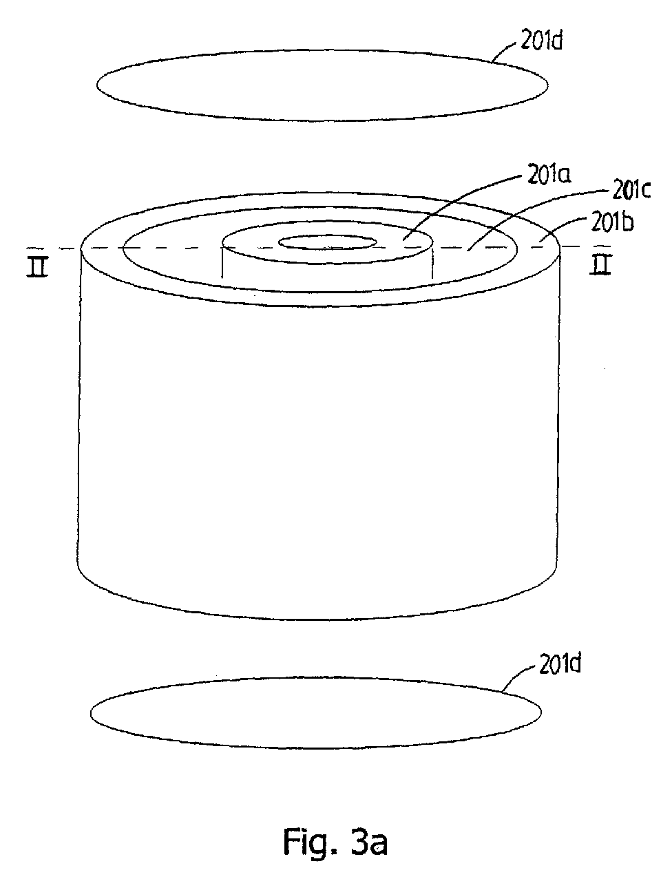
- the actuator 201 comprises shielding plates 201d which are positioned on a distance with respect to the axial element 201a and 201b.
- the shielding plates 201d are positioned axially with respect to the elements of the actuator and are of a circular shape.
- a diameter of the shielding plates 201d is preferably substantially equal to or somewhat larger than a diameter of the respective actuator or at least not substantially smaller than an inner diameter of the outer element 201a of the actuator.
- the shielding plates can comprise a ferromagnetic material, such as a steel providing effective shielding with a commonly used material or a material having a high relative permeability, preferably having a value above 50.000, more preferably between 50.000 and 200.000.
- the distance between the respective shields 201d and an end of the coaxial assembly of elements 201a and 201b is preferably between 10mm and 50mm more preferably between 20mm and 40mm, the coaxial assembly having an outer diameter between 50mm and 100mm, preferably approximately 80mm.
- the shield 201d or one of the shields 201d can be connected to one of the elements 201a, 201b, such that when the respective element moves, the respective shield 201d moves simultaneously. Also, it is possible that one of the shields 201d is connected to the element 201a while the other one of the shields 201d is connected to the element 201b. In this manner it is possible to minimise a load impedance on the actuator 201 due to minimization of movement of the shields 201d with respect to the movement of the respective elements 201a, 201b of the actuator, while simultaneously providing an effective shielding in all positions of the actuators, as preferably one of the shields moves with the element.
- the shield 201d can be mechanically connected such that it moves with the outer element 201b, however can also be connected to move with the inner element 201a. It is possible that one of the elements of the actuator moves, i.e. the other one being stationary, however it is also possible that, depending on the construction in which the actuator is comprised, that the two elements move with respect to each other.
- the actuator As an alternative to the shielding plates 201d according to fig. 2a, it is also possible to provide the actuator with a shielding sleeve or shielding can, as is depicted in fig. 3b. This has also proven to provide an effective shielding of the field generated by the long stroke actuator 200 with respect to the short stroke actuator 201a.
- the can 201e comprises a bottom plate 201f for effective shielding.
- the can preferably has a diameter which is larger, preferably 10 to 50 mm larger than a diameter of the shielded actuator, the diameter of the shielding being restricted in general by building volume restrictions in the apparatus.
- the shielding of the actuator 201 can shield a field generated by the long stroke actuator 200 as described above, however it also has the effect of diminishing a field by the other short stroke actuator 202. It is possible that only the actuator 201 is provided with a shielding as described above, however it is also possible that the actuator 201 as well as the actuator 202 is provided with a shielding according to the invention.
- Fig. 4a and 4b show a detailed, cross sectional view of a right side half of the actuator 201 according to fig. 2 showing a half of the element 201a and a half of the element 201b. Also, fig. 4a and 4b indicates further parts, such as a coil 201f and a sensor element 201g which form part of an embodiment of the actuator according to the invention.
- Fig. 4a the actuator is shown without shields, while in fig. 4b the actuator is shown comprising two shield plates 201d.
- a pattern of field lines is altered with as compared to fig. 4a.
- the positioning system according to the invention can not only be applied in a lithographic apparatus, but also in any other positioning system providing similar effects and advantages.
Landscapes
- Engineering & Computer Science (AREA)
- Physics & Mathematics (AREA)
- General Physics & Mathematics (AREA)
- Combustion & Propulsion (AREA)
- Electromagnetism (AREA)
- Power Engineering (AREA)
- Chemical & Material Sciences (AREA)
- Health & Medical Sciences (AREA)
- Epidemiology (AREA)
- Public Health (AREA)
- Life Sciences & Earth Sciences (AREA)
- Atmospheric Sciences (AREA)
- Environmental & Geological Engineering (AREA)
- Exposure And Positioning Against Photoresist Photosensitive Materials (AREA)
- Exposure Of Semiconductors, Excluding Electron Or Ion Beam Exposure (AREA)
Abstract
A lithographic apparatus comprises a positioning system comprising a first and second
electromagnetic actuator. Each actuator comprises two mutually co-operating
electromagnetical elements which are movable with respect to one another due to force
acting on the elements of the respective actuator. At least one of the actuators comprises a
shield for shielding the actuator from a field generated by the other actuator. In this
manner, a disturbance force due to the field is prevented to act on the shielded actuator.
The invention also comprises a positioning system comprising such actuators.
Description
- The invention relates to a lithographic apparatus, a device manufacturing method and a positioning system.
- A lithographic apparatus is a machine that applies a desired pattern onto a target portion of a substrate. Lithographic apparatus can be used, for example, in the manufacture of integrated circuits (ICs). In that circumstance, a patterning means, such as a mask, may be used to generate a circuit pattern corresponding to an individual layer of the IC, and this pattern can be imaged onto a target portion (e.g. comprising part of, one or several dies) on a substrate (e.g. a silicon wafer) that has a layer of radiation-sensitive material (resist). In general, a single substrate will contain a network of adjacent target portions that are successively exposed. Known lithographic apparatus include so-called steppers, in which each target portion is irradiated by exposing an entire pattern onto the target portion in one go, and so-called scanners, in which each target portion is irradiated by scanning the pattern through the projection beam in a given direction (the "scanning"-direction) while synchronously scanning the substrate parallel or anti-parallel to this direction.
- Known lithographic apparatus in general comprise positioning systems for positioning one or more elements of the apparatus. The elements can for example be a (part of an) illumination system, a (part of a) support structure, a (part of a) substrate table or any other suitable constituting element of the lithographic apparatus. The positioning systems frequently comprise a plurality of actuators, e.g. separate actuators for different directions, however it is also possible that two or more actuators are applied for a same direction, e.g. an actuator for a course, long stroke positioning and an actuator for a fine, short stroke positioning. Also, one or more of the actuators can function as a gravity compensation to compensate forces acting on parts of the lithographic apparatus due to gravity.
- Frequently, the actuators make use of a magnetic actuator, such as linear motor, a magnetic gravity compensator, a motor (e.g. a voice oil or lorentz actuator) etc..
- The inventor has recognised the problem that a field generated by one of the actuators, such as a magnetic or electromagnetic field, acts on another one of the actuators, the actuators thus influencing each other. The field generated by the one of the actuators in its operative condition results in a force acting on the other one of the actuators, and thus in a disturbance or error of the other one of the actuators.
- It is object of the present invention to increase accuracy of the lithographic apparatus and to provide a positioning system having a high accuracy.
- According to an aspect of the invention, there is provided a lithographic apparatus comprising:
- an illumination system for providing a projection beam of radiation;
- a support structure for supporting patterning means, the patterning means serving to impart the projection beam with a pattern in its cross-section;
- a substrate table for holding a substrate; and
- a projection system for projecting the patterned beam onto a target portion of the substrate, the lithographic apparatus comprising a first and a second electromagnetic actuator each comprising two mutually cooperating (such as interacting) electromagnetical elements which are movable with respect to one another due to a force acting on the elements of the respective actuator, the force being caused by a field generated by the actuator, characterised in that
- Due to the shield, it is at least partly prevented that an actuator is subjected to a field generated by the other one of the actuators or by another (moving or not moving) magnetic part, such as a ferromagnetic or electromagnetic part, and thus that a disturbance force due to the field acts on the one of the actuators. The shield reduces a strength of the field in a relevant part of the one of the actuators, the field being generated by the other one of the actuators. Due to the reduction of this field in the one of the actuators, the influence of the field on the electromagnetical elements of the one of the actuator will be reduced, and consequently the force acting between the elements of the one of the actuators due to this field will be reduced. Further, the shielding at least partly prevents the shielded actuator from disturbing its surrounding.
- The shielding per se is known, and widely applied for e.g. shielding electronic circuits from electromagnetic interference. According to the invention however, the shielding is used to at least partly prevent a force from acting on an actuator, the force being caused by a field generated by an other actuator and vice versa.
- The electromagnetical (or electromechanical) elements, advantageously comprise one or more of a group comprising a coil, a permanent magnet, a metal, a ceramic and a plastic for coating.
- As will be appreciated by the skilled person the actuator comprising the two mutually cooperating electromagnetical elements can comprise any combination of such elements which leads to a configuration in operation creating a force acting between the respective elements of such actuator.
- The shield can comprise a ferromagnetic material, such as a steel or a material having a high relative permeability (µ), preferably having a value above 50.000, more preferably between 50.000 and 200.000. An advantage is that such material provides an effective shielding while e.g. a steel is easy to fabricate and can easily be used in so called "clean" environments. Further, a saturation of is high, which has proven to be advantageous. With a material having a high relative permeability, a shielding will be improved, a value of the relative permeability above 50.000 and preferably not more than 200.000 has proven to be advantageous, as it provides effective shielding while largely avoiding a saturation of the shielding material.
- Advantageously, at least one of the electromagnetical actuators comprises a coaxial assembly of the two mutually cooperating electromagnetical elements, the shield preferably being coaxial with the assembly and located at a distance from the coaxial assembly. When, the shield is located coaxial with the coaxial assembly of the electromagnetical elements, this provides for an effective shielding, as the shield effectively reduces a strength of the field to be shielded in an annular space between the two mutually co-operating electromagnetical elements.
- In a practical embodiment which has proven to give satisfactory results, the distance is between 10mm and 50mm, preferably 20mm and 40mm, the coaxial assembly having an outer diameter between 50mm and 100mm, preferably substantially 80mm. In a practical embodiment, in general a dimension of the shield is preferably in a same order of magnitude as a dimension of the actuators.
- Advantageously the shield comprises at least one substantially circular plate or sleeve. The substantially circular plate or sleeve has proven to provide adequate results with an actuator which comprises a coaxial assembly of elements. In the case of the circular plate, the plate is advantageously located coaxial with the assembly and at a distance therefrom, while in case that the shield comprises a sleeve, the sleeve is advantageously located coaxial and surrounding at least a part of the actuator. Advantageously, a diameter of the shield is approximately equal to a diameter of the coaxial assembly. It is preferred, for optimum shielding, that the sleeve comprises a plate closed end at an end facing the other one of the actuators. Alternatively, the shield can have any other suitable form, such as a box or a circular plate.
- Advantageously, the shield or a part thereof is mechanically connected to one of the mutually co-operating electromagnetical elements. As the shield is mechanically connected to one of the mutually co-operating electromagnetical elements, the shield moves, upon movement of the respective electromagnetical element, with that element. Alternatively, it is possible that the shield, or shields are located fixedly, and thus do not move with one or more of the co-operating elements, when these elements move. By suitably selecting a set up in which one ore more shields move or do not move with one or more of the elements, a balance can be found between an effective shielding on the one hand which mostly requires a movement of the shield with one or more of the elements, and an avoidance of providing extra forces on an stator or mover of the actuator, which will be due to movements of the shield.
- The same objectives and advantages can be achieved with, and the same or similar preferred embodiments can be applied with the device manufacturing method according to the invention, which to this end comprises the steps of:
- providing a substrate;
- providing a projection beam of radiation using an illumination system;
- using patterning means to impart the projection beam with a pattern in its cross-section;
- projecting the patterned beam of radiation onto a target portion of the substrate;
- providing a first and a second electromagnetic actuator each comprising two mutually cooperating electromagnetical elements which are movable with respect to one another due to a force acting on the elements of the respective actuator, the force being caused by a field generated by the actuator, for at least partly positioning one or more of a group comprising the substrate, the illumination system, and the patterning means or any other structure cooperating with one of more of the group, characterised by, shielding one of the actuators from a second field generated by the other one of the actuators or generated by another magnetic part, for at least partly preventing a disturbance force due to the second field from acting on the one of the actuators.
- Also, the same or similar effects are achievable with the positioning system according to the invention, comprising a first and a second electromagnetic actuator each comprising two mutually cooperating electromagnetical elements which are movable with respect to one another due to a force acting on the elements of the respective actuator, the force being caused by a field generated by the actuator, characterised in that, at least one of the actuators comprises a shield for shielding the one of the actuators from a second field generated by the other one of the actuators or generated by another magnetic part, for at least partly preventing a disturbance force due to the second field from acting on the one of the actuators.
- Although specific reference may be made in this text to the use of lithographic apparatus in the manufacture of ICs, it should be understood that the lithographic apparatus described herein may have other applications, such as the manufacture of integrated optical systems, guidance and detection patterns for magnetic domain memories, liquid-crystal displays (LCDs), thin-film magnetic heads, etc. The skilled artisan will appreciate that, in the context of such alternative applications, any use of the terms "wafer" or "die" herein may be considered as synonymous with the more general terms "substrate" or "target portion", respectively. The substrate referred to herein may be processed, before or after exposure, in for example a track (a tool that typically applies a layer of resist to a substrate and develops the exposed resist) or a metrology or inspection tool. Where applicable, the disclosure herein may be applied to such and other substrate processing tools. Further, the substrate may be processed more than once, for example in order to create a multi-layer IC, so that the term substrate used herein may also refer to a substrate that already contains multiple processed layers.
- The terms "radiation" and "beam" used herein encompass all types of electromagnetic radiation, including ultraviolet (UV) radiation (e.g. having a wavelength of 365, 248, 193, 157 or 126 nm) and extreme ultra-violet (EUV) radiation (e.g. having a wavelength in the range of 5-20 nm), as well as particle beams, such as ion beams or electron beams.
- The term "patterning means" used herein should be broadly interpreted as referring to means that can be used to impart a projection beam with a pattern in its cross-section such as to create a pattern in a target portion of the substrate. It should be noted that the pattern imparted to the projection beam may not exactly correspond to the desired pattern in the target portion of the substrate. Generally, the pattern imparted to the projection beam will correspond to a particular functional layer in a device being created in the target portion, such as an integrated circuit.
- Patterning means may be transmissive or reflective. Examples of patterning means include masks, programmable mirror arrays, and programmable LCD panels. Masks are well known in lithography, and include mask types such as binary, alternating phase-shift, and attenuated phase-shift, as well as various hybrid mask types. An example of a programmable mirror array employs a matrix arrangement of small mirrors, each of which can be individually tilted so as to reflect an incoming radiation beam in different directions; in this manner, the reflected beam is patterned. In each example of patterning means, the support structure may be a frame or table, for example, which may be fixed or movable as required and which may ensure that the patterning means is at a desired position, for example with respect to the projection system. Any use of the terms "reticle" or "mask" herein may be considered synonymous with the more general term "patterning means".
- The term "projection system" used herein should be broadly interpreted as encompassing various types of projection system, including refractive optical systems, reflective optical systems, and catadioptric optical systems, as appropriate for example for the exposure radiation being used, or for other factors such as the use of an immersion fluid or the use of a vacuum. Any use of the term "lens" herein may be considered as synonymous with the more general term "projection system".
- The illumination system may also encompass various types of optical components, including refractive, reflective, and catadioptric optical components for directing, shaping, or controlling the projection beam of radiation, and such components may also be referred to below, collectively or singularly, as a "lens".
- The lithographic apparatus may be of a type having two (dual stage) or more substrate tables (and/or two or more mask tables). In such "multiple stage" machines the additional tables may be used in parallel, or preparatory steps may be carried out on one or more tables while one or more other tables are being used for exposure.
- The lithographic apparatus may also be of a type wherein the substrate is immersed in a liquid having a relatively high refractive index, e.g. water, so as to fill a space between the final element of the projection system and the substrate. Immersion liquids may also be applied to other spaces in the lithographic apparatus, for example, between the mask and the first element of the projection system. Immersion techniques are well known in the art for increasing the numerical aperture of projection systems.
- Embodiments of the invention will now be described, by way of example only, with reference to the accompanying schematic drawings in which corresponding reference symbols indicate corresponding parts, and in which:
- Fig. 1 depicts an embodiment of a lithographic apparatus;
- Fig. 2 depicts a cross sectional view of an embodiment of positioning actuators of the lithographic apparatus according to fig. 1;
- Fig. 3a and fig. 3b depict a detailed, perspective view of an actuator according to fig. 2; and
- Fig. 4a and 4b provide a graphical view of field lines in and around the actuator without and with shielding.
- Figure 1 schematically depicts a lithographic apparatus according to a particular embodiment of the invention. The apparatus comprises:
- an illumination system (illuminator) IL for providing a projection beam PB of radiation (e.g. UV or EUV radiation).
- a first support structure (e.g. a mask table) MT for supporting patterning means (e.g. a mask) MA and connected to first positioning means PM for accurately positioning the patterning means with respect to item PL;
- a substrate table (e.g. a wafer table) WT for holding a substrate (e.g. a resist-coated wafer) W and connected to second positioning means PW for accurately positioning the substrate with respect to item PL; and
- a projection system (e.g. a reflective projection lens) PL for imaging a pattern imparted to the projection beam PB by patterning means MA onto a target portion C (e.g. comprising one or more dies) of the substrate W.
- As here depicted, the apparatus is of a reflective type (e.g. employing a reflective mask or a programmable mirror array of a type as referred to above). Alternatively, the apparatus may be of a transmissive type (e.g. employing a transmissive mask).
- The illuminator IL receives a beam of radiation from a radiation source SO. The source and the lithographic apparatus may be separate entities, for example when the source is a plasma discharge source. In such cases, the source is not considered to form part of the lithographic apparatus and the radiation beam is generally passed from the source SO to the illuminator IL with the aid of a radiation collector comprising for example suitable collecting mirrors and/or a spectral purity filter. In other cases the source may be integral part of the apparatus, for example when the source is a mercury lamp. The source SO and the illuminator IL, may be referred to as a radiation system.
- The illuminator IL may comprise adjusting means for adjusting the angular intensity distribution of the beam. Generally, at least the outer and/or inner radial extent (commonly referred to as σ-outer and σ-inner, respectively) of the intensity distribution in a pupil plane of the illuminator can be adjusted. The illuminator provides a conditioned beam of radiation, referred to as the projection beam PB, having a desired uniformity and intensity distribution in its cross-section.
- The projection beam PB is incident on the mask MA, which is held on the mask table MT. Being reflected by the mask MA, the projection beam PB passes through the lens PL, which focuses the beam onto a target portion C of the substrate W. With the aid of the second positioning means PW and position sensor IF2 (e.g. an interferometric device), the substrate table WT can be moved accurately, e.g. so as to position different target portions C in the path of the beam PB. Similarly, the first positioning means PM and position sensor IF1 can be used to accurately position the mask MA with respect to the path of the beam PB, e.g. after mechanical retrieval from a mask library, or during a scan. In general, movement of the object tables MT and WT will be realized with the aid of a long-stroke module (coarse positioning) and a short-stroke module (fine positioning), which form part of the positioning means PM and PW. However, in the case of a stepper (as opposed to a scanner) the mask table MT may be connected to a short stroke actuator only, or may be fixed. Mask MA and substrate W may be aligned using mask alignment marks M1, M2 and substrate alignment marks P1, P2.
- The depicted apparatus can be used in the following preferred modes:
- 1. In step mode, the mask table MT and the substrate table WT are kept essentially stationary, while an entire pattern imparted to the projection beam is projected onto a target portion C in one go (i.e. a single static exposure). The substrate table WT is then shifted in the X and/or Y direction so that a different target portion C can be exposed. In step mode, the maximum size of the exposure field limits the size of the target portion C imaged in a single static exposure.
- 2. In scan mode, the mask table MT and the substrate table WT are scanned synchronously while a pattern imparted to the projection beam is projected onto a target portion C (i.e. a single dynamic exposure). The velocity and direction of the substrate table WT relative to the mask table MT is determined by the (de-)magnification and image reversal characteristics of the projection system PL. In scan mode, the maximum size of the exposure field limits the width (in the non-scanning direction) of the target portion in a single dynamic exposure, whereas the length of the scanning motion determines the height (in the scanning direction) of the target portion.
- 3. In another mode, the mask table MT is kept essentially stationary holding a programmable patterning means, and the substrate table WT is moved or scanned while a pattern imparted to the projection beam is projected onto a target portion C. In this mode, generally a pulsed radiation source is employed and the programmable patterning means is updated as required after each movement of the substrate table WT or in between successive radiation pulses during a scan. This mode of operation can be readily applied to maskless lithography that utilizes programmable patterning means, such as a programmable mirror array of a type as referred to above.
-
- Combinations and/or variations on the above described modes of use or entirely different modes of use may also be employed.
- Fig. 2 highly systematically shows a part of a positioning system comprised in the lithographic apparatus according to fig. 1. The positioning system comprises a
long stroke positioner 200, further in this embodiment two short stroke positioners, 201 and 202 respectively have been shown. Of thelong stroke positioner 200, an array ofpermanent magnets long stroke actuator 200, and co-operate with another electromagnetical element (not shown) to form a linear motor in a manner known as such to the person skilled in the art. Of theshort stroke actuator actuator 201 comprises a first annularmagnetic element 201a and a second annularmagnetic element 201b co-operating with the firstannular element 201a. For clarity purposes it is indicated that the cross sectional view of theactuators elements element 201b is movable with respect toelement 201a,element 202b is movable with respect toelement 202a and a second element (not shown) of thelong stroke actuator 200 is movable with respect to the array ofpermanent magnets 200 forming the other element of the long stroke actuator. As schematically shown in fig. 2, each of theactuators long stroke actuator 200 has effect on one or more of theshort stroke actuators long stroke actuator 200, a field results in one or more of theshort stroke actuators elements actuator 201 and theelements actuator 202. This force results in a position error, acceleration error, or any other position related disturbance in the respectiveshort stroke actuator - According to the invention, as will now be explained with reference to fig. 3, the
short stroke actuator long stroke actuator 200 from entering azone 201c between therespective elements actuator 200 in this zone. To this end, theactuator 201 comprises shieldingplates 201d which are positioned on a distance with respect to theaxial element shielding plates 201d are positioned axially with respect to the elements of the actuator and are of a circular shape. A diameter of theshielding plates 201d is preferably substantially equal to or somewhat larger than a diameter of the respective actuator or at least not substantially smaller than an inner diameter of theouter element 201a of the actuator. The shielding plates can comprise a ferromagnetic material, such as a steel providing effective shielding with a commonly used material or a material having a high relative permeability, preferably having a value above 50.000, more preferably between 50.000 and 200.000. The distance between therespective shields 201d and an end of the coaxial assembly ofelements shield 201d or one of theshields 201d can be connected to one of theelements respective shield 201d moves simultaneously. Also, it is possible that one of theshields 201d is connected to theelement 201a while the other one of theshields 201d is connected to theelement 201b. In this manner it is possible to minimise a load impedance on theactuator 201 due to minimization of movement of theshields 201d with respect to the movement of therespective elements lower element 201d is mechanically connected to the outercoaxial element 201b of theactuator 201, a distance between the outercoaxial element 201b and thelower shield 201d is constant when theouter element 201b moves with respect to theinner element 201a. Thus, an effect of the shielding by thelower shielding plate 201d is virtually independent of a position of theouter element 201b. In this example, theshield 201d can be mechanically connected such that it moves with theouter element 201b, however can also be connected to move with theinner element 201a. It is possible that one of the elements of the actuator moves, i.e. the other one being stationary, however it is also possible that, depending on the construction in which the actuator is comprised, that the two elements move with respect to each other. - As an alternative to the
shielding plates 201d according to fig. 2a, it is also possible to provide the actuator with a shielding sleeve or shielding can, as is depicted in fig. 3b. This has also proven to provide an effective shielding of the field generated by thelong stroke actuator 200 with respect to theshort stroke actuator 201a. Preferably, to improve shielding, thecan 201e comprises abottom plate 201f for effective shielding. In the example and dimensions as given with reference to the actuator according to fig. 2a, the can preferably has a diameter which is larger, preferably 10 to 50 mm larger than a diameter of the shielded actuator, the diameter of the shielding being restricted in general by building volume restrictions in the apparatus. - The shielding of the
actuator 201 can shield a field generated by thelong stroke actuator 200 as described above, however it also has the effect of diminishing a field by the othershort stroke actuator 202. It is possible that only theactuator 201 is provided with a shielding as described above, however it is also possible that theactuator 201 as well as theactuator 202 is provided with a shielding according to the invention. - An effect of the shielding will now be described with reference to fig. 4a and 4b. Fig. 4a and 4b show a detailed, cross sectional view of a right side half of the
actuator 201 according to fig. 2 showing a half of theelement 201a and a half of theelement 201b. Also, fig. 4a and 4b indicates further parts, such as acoil 201f and a sensor element 201g which form part of an embodiment of the actuator according to the invention. Fig. 4a, the actuator is shown without shields, while in fig. 4b the actuator is shown comprising twoshield plates 201d. As can be observed from fig. 4b a pattern of field lines is altered with as compared to fig. 4a. - The positioning system according to the invention can not only be applied in a lithographic apparatus, but also in any other positioning system providing similar effects and advantages.
- While specific embodiments of the invention have been described above, it will be appreciated that the invention may be practised otherwise than as described. The description is not intended to limit the invention.
Claims (14)
- A lithographic apparatus comprising:the lithographic apparatus comprising a first and a second electromagnetic actuator each comprising two mutually cooperating electromagnetical elements which are movable with respect to one another due to a force acting on the elements of the respective actuator, the force being caused by a field generated by the actuator, characterised in that,an illumination system for providing a projection beam of radiation;a support structure for supporting patterning means, the patterning means serving to impart the projection beam with a pattern in its cross-section;a substrate table for holding a substrate; anda projection system for projecting the patterned beam onto a target portion of the substrate,
at least one of the actuators comprises a shield for shielding the one of the actuators from a second field generated by the other one of the actuators or generated by another magnetic part of the apparatus, for at least partly preventing a disturbance force due to the second field from acting on the one of the actuators. - The lithographic apparatus according to claim 1, wherein the electromagnetical elements comprise one or more of a group comprising a coil, a permanent magnet, a metal, a ceramic, and a plastic for coating.
- The lithographic apparatus according to claim 1 or 2, wherein the shield comprises a ferromagnetic material
- The lithographic apparatus according to claim 3, wherein the shield comprises a steel.
- The lithographic apparatus according to claim 3, wherein the shield comprises a material having a high relative permeability.
- The lithographic apparatus according to claim 5, wherein a value of the relative permeability is above 50000, preferably between 50000 and 200000.
- The lithographic apparatus according to any of the preceding claims, wherein at least one of the electromagnetical actuators comprises a coaxial assembly of the two mutually cooperating electromagnetical elements, the shield preferably being coaxial with the assembly and located at a distance from the coaxial assembly.
- The lithographic apparatus according to claim 7, wherein the distance is between 10mm and 50mm, preferably 20mm and 40mm, the coaxial assembly having an outer diameter between 50mm and 100mm, preferably substantially 80mm.
- The lithographic apparatus according to any of the preceding claims, wherein the shield comprises at least one substantially circular plate.
- The lithographic apparatus according to any of the preceding claims, wherein the shield comprises a sleeve.
- The lithographic apparatus according to claim 9 or 10, wherein a diameter of the shield is approximately equal to a diameter of the coaxial assembly.
- The lithographic apparatus according to any of the preceding claims, wherein the shield or a part thereof is mechanically connected to one of the mutually cooperating electromagnetical elements.
- A device manufacturing method comprising the steps of:providing a substrate;providing a projection beam of radiation using an illumination system;using patterning means to impart the projection beam with a pattern in its cross-section; andprojecting the patterned beam of radiation onto a target portion of the substrate,providing a first and a second electromagnetic actuator each comprising two mutually cooperating electromagnetical elements which are movable with respect to one another due to a force acting on the elements of the respective actuator, the force being caused by a field generated by the actuator, for at least partly positioning one or more of a group comprising the substrate, the illumination system, and the patterning means or any other structure cooperating with one of more of the group, characterised by,shielding one of the actuators from a second field generated by the other one of the actuators or generated by another magnetic part, for at least partly preventing a disturbance force due to the second field from acting on the one of the actuators.
- A positioning system comprising a first and a second electromagnetic actuator each comprising two mutually cooperating electromagnetical elements which are movable with respect to one another due to a force acting on the elements of the respective actuator, the force being caused by a field generated by the actuator, characterised in that,
at least one of the actuators comprises a shield for shielding the one of the actuators from a second field generated by the other one of the actuators or generated by another magnetic part, for at least partly preventing a disturbance force due to the second field from acting on the one of the actuators.
Priority Applications (3)
| Application Number | Priority Date | Filing Date | Title |
|---|---|---|---|
| EP03078282A EP1524556A1 (en) | 2003-10-17 | 2003-10-17 | Lithographic apparatus, device manufacturing method and positioning system |
| JP2004301723A JP2005123629A (en) | 2003-10-17 | 2004-10-15 | Lithographic equipment, device manufacturing method, and positioning system |
| US10/964,818 US7224429B2 (en) | 2003-10-17 | 2004-10-15 | Lithographic apparatus, device manufacturing method and positioning system |
Applications Claiming Priority (1)
| Application Number | Priority Date | Filing Date | Title |
|---|---|---|---|
| EP03078282A EP1524556A1 (en) | 2003-10-17 | 2003-10-17 | Lithographic apparatus, device manufacturing method and positioning system |
Publications (1)
| Publication Number | Publication Date |
|---|---|
| EP1524556A1 true EP1524556A1 (en) | 2005-04-20 |
Family
ID=34354529
Family Applications (1)
| Application Number | Title | Priority Date | Filing Date |
|---|---|---|---|
| EP03078282A Withdrawn EP1524556A1 (en) | 2003-10-17 | 2003-10-17 | Lithographic apparatus, device manufacturing method and positioning system |
Country Status (3)
| Country | Link |
|---|---|
| US (1) | US7224429B2 (en) |
| EP (1) | EP1524556A1 (en) |
| JP (1) | JP2005123629A (en) |
Cited By (3)
| Publication number | Priority date | Publication date | Assignee | Title |
|---|---|---|---|---|
| EP1944650A3 (en) * | 2007-01-15 | 2008-07-30 | Canon Kabushiki Kaisha | Stage device, exposure apparatus and device manufacturing method |
| NL2001216C2 (en) * | 2008-01-25 | 2009-07-30 | Dams Beheer B V J | Magnetic actuator. |
| CN113471112A (en) * | 2021-07-16 | 2021-10-01 | 上海隐冠半导体技术有限公司 | Magnetic suspension gravity compensation device and micro-motion platform |
Families Citing this family (8)
| Publication number | Priority date | Publication date | Assignee | Title |
|---|---|---|---|---|
| US7348752B1 (en) * | 2006-09-20 | 2008-03-25 | Asml Netherlands B.V. | Stage apparatus and lithographic apparatus |
| WO2011103324A2 (en) | 2010-02-17 | 2011-08-25 | Viking At, Llc | Smart material actuator capable of operating in three dimensions |
| WO2013113632A2 (en) | 2012-02-03 | 2013-08-08 | Asml Netherlands B.V. | A stage system and a lithographic apparatus |
| US20140091649A1 (en) * | 2012-10-02 | 2014-04-03 | Remy Technologies, Llc | Electromagnetic interference shield and balance ring for electrical machine |
| WO2015100280A1 (en) | 2013-12-24 | 2015-07-02 | Viking At, Llc | Mechanically amplified smart material actuator utilizing layered web assembly |
| WO2015104099A1 (en) * | 2014-01-13 | 2015-07-16 | Asml Netherlands B.V. | Actuation mechanism, optical apparatus and lithography apparatus |
| CN105988304B (en) * | 2015-02-28 | 2018-10-16 | 上海微电子装备(集团)股份有限公司 | A kind of adjustable magnetic buoyancy gravity compensator |
| KR20250021636A (en) * | 2018-07-04 | 2025-02-13 | 에이에스엠엘 네델란즈 비.브이. | Apparatus for Positioning and Clamped Curing |
Citations (5)
| Publication number | Priority date | Publication date | Assignee | Title |
|---|---|---|---|---|
| EP1001512A2 (en) * | 1998-11-10 | 2000-05-17 | Asm Lithography B.V. | Actuator and transducer |
| US20020074516A1 (en) * | 2000-12-08 | 2002-06-20 | Novak W. Thomas | Positioning stage with stationary and movable magnet tracks |
| EP1267209A1 (en) * | 2001-06-13 | 2002-12-18 | James E. Sanford | Maskless exposure system using mems devices |
| JP2003088088A (en) * | 2001-09-13 | 2003-03-20 | Jeol Ltd | Linear motor and moving device and charged particle beam device |
| US20030155820A1 (en) * | 2002-02-18 | 2003-08-21 | Kabushiki Kaisha Yaskawa Denki | Magnetically shielded linear motors, and stage apparatus comprising same |
Family Cites Families (1)
| Publication number | Priority date | Publication date | Assignee | Title |
|---|---|---|---|---|
| JP3484684B2 (en) * | 1994-11-01 | 2004-01-06 | 株式会社ニコン | Stage apparatus and scanning type exposure apparatus |
-
2003
- 2003-10-17 EP EP03078282A patent/EP1524556A1/en not_active Withdrawn
-
2004
- 2004-10-15 JP JP2004301723A patent/JP2005123629A/en active Pending
- 2004-10-15 US US10/964,818 patent/US7224429B2/en not_active Expired - Lifetime
Patent Citations (5)
| Publication number | Priority date | Publication date | Assignee | Title |
|---|---|---|---|---|
| EP1001512A2 (en) * | 1998-11-10 | 2000-05-17 | Asm Lithography B.V. | Actuator and transducer |
| US20020074516A1 (en) * | 2000-12-08 | 2002-06-20 | Novak W. Thomas | Positioning stage with stationary and movable magnet tracks |
| EP1267209A1 (en) * | 2001-06-13 | 2002-12-18 | James E. Sanford | Maskless exposure system using mems devices |
| JP2003088088A (en) * | 2001-09-13 | 2003-03-20 | Jeol Ltd | Linear motor and moving device and charged particle beam device |
| US20030155820A1 (en) * | 2002-02-18 | 2003-08-21 | Kabushiki Kaisha Yaskawa Denki | Magnetically shielded linear motors, and stage apparatus comprising same |
Non-Patent Citations (1)
| Title |
|---|
| PATENT ABSTRACTS OF JAPAN vol. 2003, no. 07 3 July 2003 (2003-07-03) * |
Cited By (7)
| Publication number | Priority date | Publication date | Assignee | Title |
|---|---|---|---|---|
| EP1944650A3 (en) * | 2007-01-15 | 2008-07-30 | Canon Kabushiki Kaisha | Stage device, exposure apparatus and device manufacturing method |
| US7932646B2 (en) | 2007-01-15 | 2011-04-26 | Canon Kabushiki Kaisha | Exposure apparatus with a stage, driving unit,and force applying unit having a separate magnetic shield |
| NL2001216C2 (en) * | 2008-01-25 | 2009-07-30 | Dams Beheer B V J | Magnetic actuator. |
| WO2009093907A1 (en) * | 2008-01-25 | 2009-07-30 | J. Dams Beheer B.V. | Magnectic actuator |
| US8803644B2 (en) | 2008-01-25 | 2014-08-12 | J. Dams Beheer B.V. | Magnetic actuator |
| CN113471112A (en) * | 2021-07-16 | 2021-10-01 | 上海隐冠半导体技术有限公司 | Magnetic suspension gravity compensation device and micro-motion platform |
| CN113471112B (en) * | 2021-07-16 | 2024-02-20 | 上海隐冠半导体技术有限公司 | Maglev gravity compensation device and micro-motion stage |
Also Published As
| Publication number | Publication date |
|---|---|
| US20050146698A1 (en) | 2005-07-07 |
| JP2005123629A (en) | 2005-05-12 |
| US7224429B2 (en) | 2007-05-29 |
Similar Documents
| Publication | Publication Date | Title |
|---|---|---|
| US6943464B2 (en) | Lithographic apparatus and motor for use in the apparatus | |
| EP1882986B1 (en) | Lithographic apparatus with planar motor driven support | |
| US20200050115A1 (en) | Motor assembly, lithographic apparatus and device manufacturing method | |
| KR101142376B1 (en) | Lithographic apparatus and device manufacturing method | |
| US7145269B2 (en) | Lithographic apparatus, Lorentz actuator, and device manufacturing method | |
| EP2175548B1 (en) | Lithographic apparatus and Lorentz actuator | |
| EP2492928A2 (en) | Electromagnetic actuator, stage apparatus and lithographic apparatus | |
| US10310392B2 (en) | Positioning device, lithographic apparatus and device manufacturing method | |
| US7167234B2 (en) | Actuator assembly and lithographic apparatus comprising such an actuator assembly | |
| US7224429B2 (en) | Lithographic apparatus, device manufacturing method and positioning system | |
| US7259832B2 (en) | Lithographic apparatus and device manufacturing method | |
| US7348752B1 (en) | Stage apparatus and lithographic apparatus | |
| EP2132601A1 (en) | Illumination system for illuminating a patterning device and method for manufacturing an illumination system | |
| US7006199B2 (en) | Lithographic positioning device and device manufacturing method | |
| EP1530090B1 (en) | Lithographic apparatus and device manufacturing method | |
| EP1538484A1 (en) | EUV illumination system and lithographic apparatus | |
| US9293951B2 (en) | Lithographic apparatus and lorentz actuator | |
| WO2008147175A1 (en) | Lithographic apparatus and device manufacturing method | |
| US7592760B2 (en) | Lithographic apparatus and device manufacturing method | |
| US20190074756A1 (en) | Magnet array, electric coil device, displacement system, lithographic apparatus and device manufacturing method | |
| WO2013143777A2 (en) | Substrate table system, lithographic apparatus and substrate table swapping method |
Legal Events
| Date | Code | Title | Description |
|---|---|---|---|
| PUAI | Public reference made under article 153(3) epc to a published international application that has entered the european phase |
Free format text: ORIGINAL CODE: 0009012 |
|
| AK | Designated contracting states |
Kind code of ref document: A1 Designated state(s): AT BE BG CH CY CZ DE DK EE ES FI FR GB GR HU IE IT LI LU MC NL PT RO SE SI SK TR |
|
| AX | Request for extension of the european patent |
Extension state: AL LT LV MK |
|
| STAA | Information on the status of an ep patent application or granted ep patent |
Free format text: STATUS: THE APPLICATION IS DEEMED TO BE WITHDRAWN |
|
| 18D | Application deemed to be withdrawn |
Effective date: 20050218 |