EP1523205B1 - Method and system for accessing a smart card stored in a telecommunications card from a host device to which said telecommunications card is connected - Google Patents
Method and system for accessing a smart card stored in a telecommunications card from a host device to which said telecommunications card is connected Download PDFInfo
- Publication number
- EP1523205B1 EP1523205B1 EP20040447224 EP04447224A EP1523205B1 EP 1523205 B1 EP1523205 B1 EP 1523205B1 EP 20040447224 EP20040447224 EP 20040447224 EP 04447224 A EP04447224 A EP 04447224A EP 1523205 B1 EP1523205 B1 EP 1523205B1
- Authority
- EP
- European Patent Office
- Prior art keywords
- smart card
- command
- host device
- telecommunications
- buffer
- Prior art date
- Legal status (The legal status is an assumption and is not a legal conclusion. Google has not performed a legal analysis and makes no representation as to the accuracy of the status listed.)
- Expired - Lifetime
Links
Images

Classifications
-
- H—ELECTRICITY
- H04—ELECTRIC COMMUNICATION TECHNIQUE
- H04M—TELEPHONIC COMMUNICATION
- H04M17/00—Prepayment of wireline communication systems, wireless communication systems or telephone systems
- H04M17/02—Coin-freed or check-freed systems, e.g. mobile- or card-operated phones, public telephones or booths
-
- G—PHYSICS
- G06—COMPUTING OR CALCULATING; COUNTING
- G06F—ELECTRIC DIGITAL DATA PROCESSING
- G06F21/00—Security arrangements for protecting computers, components thereof, programs or data against unauthorised activity
- G06F21/30—Authentication, i.e. establishing the identity or authorisation of security principals
- G06F21/31—User authentication
- G06F21/34—User authentication involving the use of external additional devices, e.g. dongles or smart cards
- G06F21/35—User authentication involving the use of external additional devices, e.g. dongles or smart cards communicating wirelessly
-
- H—ELECTRICITY
- H04—ELECTRIC COMMUNICATION TECHNIQUE
- H04W—WIRELESS COMMUNICATION NETWORKS
- H04W8/00—Network data management
- H04W8/18—Processing of user or subscriber data, e.g. subscribed services, user preferences or user profiles; Transfer of user or subscriber data
-
- H—ELECTRICITY
- H04—ELECTRIC COMMUNICATION TECHNIQUE
- H04W—WIRELESS COMMUNICATION NETWORKS
- H04W92/00—Interfaces specially adapted for wireless communication networks
- H04W92/04—Interfaces between hierarchically different network devices
- H04W92/08—Interfaces between hierarchically different network devices between user and terminal device
Definitions
- the present invention relates to a method for accessing a smart card from a host device, such as for example a laptop or notebook PC, according to the preamble of claim 1.
- the present invention further relates to a system for accessing a smart card from a host device, such as for example a laptop or notebook PC, according to the preamble of claim 7.
- a host device such as for example a laptop or notebook PC
- USB dongle Today, smart card manufacturers make use of their own developed USB dongle containing a smart card reader.
- the PCSC-driver and the plug and play mechanism of Windows provide the OS with all information which enables any application running on the host device to utilise the smart card connected via the USB dongle for its own purpose.
- telecommunications cards are known, which enable the host device to communicate via a telecommunication network.
- these telecommunication cards carry a smart card with user specific information and have a smart card reader on board.
- this smart card can only be used for user identification purposes towards the network operator.
- a smart IC card system comprising an IC card and an IC card reader for executing financial transactions.
- an access command is provided on the host device, which is provided for instructing the command interpreter of the telecommunications card to pass on a command, which originates from the host device and is attached to the access command, directly to the smart card.
- a command which originates from the host device and is attached to the access command, directly to the smart card.
- an application command is then attached to the access command and this combination is forwarded to the command interpreter, who is thus instructed to pass on the application command to the smart card.
- the response which is given by the smart card to the application command is stored in a buffer which is accessible towards the host device, so that the response can be read and used on the host device for further processing.
- the use of the smart card reader on board the telecommunications card as generic smart card reader towards the host device has the advantage that the need for a separate smart card reader, such as a USB dongle, is avoided. As a result, the interface to which this separate smart card reader would be connected, such as a USB gate, remains free for connecting other devices. Furthermore, the user does no longer need to purchase separated devices for telecommunication and smart card access.
- the access command is included in a driver which is provided on the host device. This makes the access command available to any application running on the host device, so that any such application can gain access to the smart card stored in the telecommunications card by simply attaching its application command to the access command defined in the driver.
- the accessibility to the smart card stored in the telecommunications card for applications running on the host device has the advantage that this smart card can be used for user authentication purposes on the host device instead of a smart card connected via a separate reader. This can not only avoid the need for the user to purchase two different smart cards for different applications, but also makes the one smart card available for the applications running on the host device while in use as user identification module towards the telecommunications network operator. As a result, the smart card can be used for authentication in internet sale, WLAN authentication, VPN security, banking wire transfers, user identification upon power-up of the host device, etc.
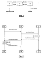
- Figure 1 schematically shows the interaction between the user, the host device, the telecommunications card and the telecommunications network with the method of the invention.
- FIG. 2 shows how an access command AT+CSIM is used, according to the invention, by an application on the host device for verifying personal code information from the smart card.
- Figure 3 shows how a personal code request command AT+CPIN / AT+CPIN? is used according to the invention by the modem for verifying personal code information from the smart card.
- the method of the invention enables access to a smart card SIM stored in a telecommunications card MT from a host device TE.
- the telecommunications card MT enables telecommunication between the host device TE and a telecommunications network which requires a smart card SIM for user identification, which may for instance include one or more of the following 3GPP Access Technologies: GSM/GPRS/UMTS or WLAN 802.11abg and 802.16.
- the telecommunications card MT comprises a command interpreter TA for interpreting host device commands and a modem ME with associated smart card reader for reading the smart card SIM.
- smart card includes "SIM”, “USIM” (3GPP UMTS SIM) and “UICC” (3GPP2 CDMA1x and CDMA2K) and any other smart card used for user identification purposes known to the person skilled in the art.
- SIM SIM
- USIM 3GPP UMTS SIM
- UICC 3GPP2 CDMA1x and CDMA2K
- an access command AT+CSIM is presented on the host device, for example in a PCSC driver for Windows XP.
- This access command - when executed - instructs the command interpreter TA to pass on any attached APDU (Application Protocol Data Unit) command originating from the host device TE to the smart card reader in the ME.
- Any response from the SIM to such an APDU is buffered in a first buffer which is accessible to the host device TE, so that the response can be read out to the host device in a next step.
- This first buffer is preferably provided on the TA, but may also be located on the ME or elsewhere on the MT.
- any exchange of information with the SIM will be done by pure APDU commands with the AT+CSIM as the sole transporter, instead of applying AT-commands in order to have access to the SIM.
- the functionality of the AT+CPIN may as well be sent by an APDU command.
- the huge advantage of employing APDU commands directly is that there is no need to translate them to AT commands, i.e. commands interpretable by the command interpreter TA.
- the standard factory drivers When the method of the invention is implemented on a Windows system, the standard factory drivers will externally be visible as normal and there will be a driver that supports the Microsoft Interface for APDU. For the APDU commands "wrapped" in the AT+CSIM command to send, a MUX Command channel is allocated, which is not being used by the Command and Data ports.
- a Smartcard compatible device driver At installation of the telecommunications card, a Smartcard compatible device driver is exposed which is acceptable to Windows as a standard Smartcard Device. This Smartcard driver can use the Windows Smartcard library and environment to process Smartcard requests from XP and hence form user(TE) applications.
- the method and algorithm of the invention can also be implemented in other operating systems known to the person skilled in the art.
- a first measure is to store smart card type data (ATR_structure) in a second buffer, preferably on the modem ME, and to include a type request command AT_OATR in the PCSC driver on the host device TE.
- ATR_structure smart card type data
- This enables the application which wants to access the SIM to first readout the smart card type data from the second buffer, assuring itself that the SIM is suitable. By buffering this information, the readout of the smart card type data and subsequently the AT_OATR will not power up or down the SIM, so that any ongoing telecommunication is not hampered. Once a valid ATR_structure is returned, AT+CSIM/APDU commands are to be sent.
- sending the AT_OATR command will return the ATR_structure information in the same way as it was sent through the SIM task on reset/start-up, but no reset/start-up occurs since the information is read from the buffer.
- the AT_OATR is implemented using the following bidirectional signals between TA and ME: each time an APEX_SIM_ATR_INFO_REQ/ALSI SIM_ATR_INFO_REQ is received, the ATR_structure is returned in the confirmation signals APEX-SIM-ATR-INFO-CNF/ALSI-SIM-ATR-INFO-CNF.
- the ATR_structure holds state information and the capabilities about the Smart card reader.
- the last member of this ATR_structure stores the capabilities of the SIM card, the ATR value.
- the ATR_structure comprises the following members: - CurrentState: contains the status of the card: Status Meaning SCARD_UNKNOWN The Smart card reader does not know the status. SCARD_ABSENT No card is currently inserted. SCARD_PRESENT A card is inserted.
- - ClkFrequency contains the standard clock frequency that the Smart card reader runs at, in KHz, encoded in little-endian format. For example, 3.58 MHz would be encoded as 3580.
- BaudRatefactors contains a byte that codes in binary the unsigned positive integers FI and DI.
- FI is the reference to a clock rate conversion factor over the bits b8 to b5.
- DI is the reference to a baud rate adjustment factor over the bits b4 to b1.
- FI and DI are referencing respectively the factors F and D. Both factors will define the standard baud rate of the Smart card reader.
- the baud rate period of the transmission clock of the data bit between the smart card and the physical interface device is called the Elementary Time Unit.
- the possible (F/D) pair values are defined in the ISO7816-3 standard.
- - PowerMgmtSupport A flag with a value of zero indicates that the reader does not support clock stop mode. Either a zero indicating that the clock will stop at a level of zero Volts, or a one indicating the clock will stop at the highest voltage level should follow the flag value of 1.
- - VoltagesSupportedList contains a list of voltages, in Volt, supported by the Smart card reader physically embedded in the ME Baseband.
- - ATR the answer to reset (ATR) information, which the smart card provides to the reader after a warm or cold reset, consists of the initial character TS followed by at most 32 characters. See the relevant ISO/IEC7816-3 and the 3GPP TS 11.11 Rel '98 specifications.
- a second measure is that the command interpreter TA takes the initiative for getting a response from the addressed memory location on the smart card.
- the problem which is solved here is that most AT+CSIM commands need to be executed in two phases of access to the SIM. Practically it means that after receiving an +CSIM/APDU command the TA is firing off immediately behind a second one: an APDU with INS code C0 or a 'GET RESPONSE', without waiting for the actual AT+CSIM/'GET RESPONSE' command, which is a lot slower.
- the TA keeps the answer from the SIM in a buffer until the TE's AT+CSIM/'GET RESPONSE' comes around and is captured by the TA.
- the TA then gives the content of the buffer as reply and clears it afterwards. If a different APDU passes by from an APDU/'GET RESPONSE' the buffer is cleared anyway.
- the smart card reader performs also other tasks than those which it receives from the TA, for example telecommunication tasks, which could involve a change of its address pointer between the receipt of the APDU and the 'GET RESPONSE'.
- the smart card reader checks its address pointer and corrects it if necessary, before reading the response and returning it to the TA.
- the procedure is in fact as follows.
- the TE sends an APDU wrapped in the AT+CSIM command to the TA, which forwards the APDU to the SIM reader.
- the APDU in fact comprises an intended address of a memory location on the SIM, from which a response is to be got.
- the SIM reader sets its address pointer to the supplied intended address, which ripples back to the TA and is stored in the third buffer.
- the TA then takes initiative and sends a 'GET RESPONSE' to the SIM reader, along with the intended address stored in the third buffer.
- the SIM reader checks its address pointer by means of the value supplied from the third buffer, i.e. the intended address, and corrects if necessary, and then gets the response from the SIM at the intended address. Finally the response is returned to the TA, where it is stored in the first buffer until the AT+CSIM/'GET RESPONSE' from the application running on the host device comes round.
- a third measure is a modification in the AT+CPIN command on the modem ME, which is used for questioning the status of the SIM's user personal codes PIN & PUK.
- the smart card comprises one or more registers CHVx for storing the PIN & PUK codes or a status thereof.
- the modem ME - when performing a personal code request command like AT+CPIN or AT+CPIN? - would refer to a copy of the CHVx registers which is created on power-up of the smart card and kept on the smart card reader.
- the modem ME always refers to the CHVx registers, since there is a possibility that their contents have been changed by an application running on the host device TE and that the copy kept on the smart card reader no longer corresponds to the actual values.
- Fig. 2 shows how use is made of the AT+CSIM/APDU command for accessing the CHVx registers.
- the Smart card reader sends an AlsiSimInsertedInd to the ME.
- the AlsiSimInsertedInd states the status of the PIN. (i.e. whether it is enabled/disabled/blocked and the number of remaining retries).
- the ME then sends an ApexSimGetChvInd to all the registered tasks to request the user(TE) to enter the PIN.
- the ME is waiting for the ApexSimGetChvRsp to come back in order to carry on the initialisation of the ME.
- the requirement is dropped in TA to have first entered the PIN code before any other AT command might be launched.
- Fig. 2 shows that the ME sends an ApexSimGetChvInd to the registered tasks. Given the ApexSimGetChvRsp never comes back, the ME does not send any AlsiSimInitialiseReq to the Smart card reader, and the ME initialisation PS stops there.
- Fig. 3 shows how 'AT+CPIN?' command is modified to force the ME initialisation PS after the registers CHVx (PIN) are verified and OK, which meets the network operators' request that the terminal should not register to the network before the PIN code is entered in good order.
- an ApexSimGetChvRsp is sent, conveying the CHV value.
- the ME receives the ApexSimGetChvRsp, the ME then sends the AlsiSimIntialiseReq to the Smart card reader.
- the Smart card reader passes the CHV1 value to the SIM (VERIFY CHV command is sent to the SIM).
- the AlsiSiminitialiseCnf comes back, and the ME carries on starting the protocol stack PS. At least entering the PIN with 'AT+CPIN' will initiate a probing first for the actual status of the PIN as if it were an 'AT+CPIN?' was requested.
- the AT+CPIN/AT+CPIN? is reserved for modem tasks, while applications on the host device need to use AT+CSIM/APDU for accessing the PIN/PUK codes on the SIM. Not only does this have the advantage of preventing that an application on the host device would interfere in telecommunication tasks performed by the protocol stack, but also that prior art applications intended for running on the modem do not need to be modified.
Landscapes
- Engineering & Computer Science (AREA)
- Computer Security & Cryptography (AREA)
- Computer Networks & Wireless Communication (AREA)
- Theoretical Computer Science (AREA)
- Computer Hardware Design (AREA)
- Software Systems (AREA)
- Physics & Mathematics (AREA)
- General Engineering & Computer Science (AREA)
- General Physics & Mathematics (AREA)
- Signal Processing (AREA)
- Telephonic Communication Services (AREA)
Description
- The present invention relates to a method for accessing a smart card from a host device, such as for example a laptop or notebook PC, according to the preamble of claim 1.
- The present invention further relates to a system for accessing a smart card from a host device, such as for example a laptop or notebook PC, according to the preamble of claim 7.
- Today, smart card manufacturers make use of their own developed USB dongle containing a smart card reader. The PCSC-driver and the plug and play mechanism of Windows provide the OS with all information which enables any application running on the host device to utilise the smart card connected via the USB dongle for its own purpose.
- On the other hand, telecommunications cards are known, which enable the host device to communicate via a telecommunication network. For enabling user identification towards the used telecommunication network, these telecommunication cards carry a smart card with user specific information and have a smart card reader on board. However, as it has been implemented up to now, this smart card can only be used for user identification purposes towards the network operator.
- From
US 5 942 738 A , a smart IC card system is known comprising an IC card and an IC card reader for executing financial transactions. - From
WO 98/27767 A1 - From
FR 2 818 764 A1 - From
DE 195 22 527 A1 a method is known for enabling communication between an application and a smart card. - It is an aim of this invention to provide a method and system for accessing the smart card stored in the telecommunications card from the host device.
- This aim is achieved by the method showing the steps of the characterising part of claim 1 and by a system according to claim 7.
- More particularly, an access command is provided on the host device, which is provided for instructing the command interpreter of the telecommunications card to pass on a command, which originates from the host device and is attached to the access command, directly to the smart card. For accessing the smart card from the host device, an application command is then attached to the access command and this combination is forwarded to the command interpreter, who is thus instructed to pass on the application command to the smart card. The response which is given by the smart card to the application command is stored in a buffer which is accessible towards the host device, so that the response can be read and used on the host device for further processing.
- The use of the smart card reader on board the telecommunications card as generic smart card reader towards the host device has the advantage that the need for a separate smart card reader, such as a USB dongle, is avoided. As a result, the interface to which this separate smart card reader would be connected, such as a USB gate, remains free for connecting other devices. Furthermore, the user does no longer need to purchase separated devices for telecommunication and smart card access.
- In a preferred embodiment of the method of the invention, the access command is included in a driver which is provided on the host device. This makes the access command available to any application running on the host device, so that any such application can gain access to the smart card stored in the telecommunications card by simply attaching its application command to the access command defined in the driver.
- The accessibility to the smart card stored in the telecommunications card for applications running on the host device has the advantage that this smart card can be used for user authentication purposes on the host device instead of a smart card connected via a separate reader. This can not only avoid the need for the user to purchase two different smart cards for different applications, but also makes the one smart card available for the applications running on the host device while in use as user identification module towards the telecommunications network operator. As a result, the smart card can be used for authentication in internet sale, WLAN authentication, VPN security, banking wire transfers, user identification upon power-up of the host device, etc.
- The invention will be further elucidated by means of the following description and the appended figures.
-
Figure 1 schematically shows the interaction between the user, the host device, the telecommunications card and the telecommunications network with the method of the invention. -
Figure 2 shows how an access command AT+CSIM is used, according to the invention, by an application on the host device for verifying personal code information from the smart card. -
Figure 3 shows how a personal code request command AT+CPIN / AT+CPIN? is used according to the invention by the modem for verifying personal code information from the smart card. - As shown in
figure 1 , the method of the invention enables access to a smart card SIM stored in a telecommunications card MT from a host device TE. The telecommunications card MT enables telecommunication between the host device TE and a telecommunications network which requires a smart card SIM for user identification, which may for instance include one or more of the following 3GPP Access Technologies: GSM/GPRS/UMTS or WLAN 802.11abg and 802.16. The telecommunications card MT comprises a command interpreter TA for interpreting host device commands and a modem ME with associated smart card reader for reading the smart card SIM. As used herein, the term smart card includes "SIM", "USIM" (3GPP UMTS SIM) and "UICC" (3GPP2 CDMA1x and CDMA2K) and any other smart card used for user identification purposes known to the person skilled in the art. The modem ME enables the telecommunication and the user identification, but is only accessible to the host device via the command interpreter TA. - In order to enable applications running on the host device TE to access the smart card SIM, an access command AT+CSIM is presented on the host device, for example in a PCSC driver for Windows XP. This access command - when executed - instructs the command interpreter TA to pass on any attached APDU (Application Protocol Data Unit) command originating from the host device TE to the smart card reader in the ME. Any response from the SIM to such an APDU is buffered in a first buffer which is accessible to the host device TE, so that the response can be read out to the host device in a next step. This first buffer is preferably provided on the TA, but may also be located on the ME or elsewhere on the MT.
- With the method of the invention, any exchange of information with the SIM will be done by pure APDU commands with the AT+CSIM as the sole transporter, instead of applying AT-commands in order to have access to the SIM. For instance the functionality of the AT+CPIN (see below) may as well be sent by an APDU command. The huge advantage of employing APDU commands directly is that there is no need to translate them to AT commands, i.e. commands interpretable by the command interpreter TA.
- When the method of the invention is implemented on a Windows system, the standard factory drivers will externally be visible as normal and there will be a driver that supports the Microsoft Interface for APDU. For the APDU commands "wrapped" in the AT+CSIM command to send, a MUX Command channel is allocated, which is not being used by the Command and Data ports. At installation of the telecommunications card, a Smartcard compatible device driver is exposed which is acceptable to Windows as a standard Smartcard Device. This Smartcard driver can use the Windows Smartcard library and environment to process Smartcard requests from XP and hence form user(TE) applications. Of course, the method and algorithm of the invention can also be implemented in other operating systems known to the person skilled in the art.
- In the following, a number of measures will be described which contribute to the functioning of the access method of the invention and prevent harm to the telecommunication operations which may occur simultaneously.
- A first measure is to store smart card type data (ATR_structure) in a second buffer, preferably on the modem ME, and to include a type request command AT_OATR in the PCSC driver on the host device TE. This enables the application which wants to access the SIM to first readout the smart card type data from the second buffer, assuring itself that the SIM is suitable. By buffering this information, the readout of the smart card type data and subsequently the AT_OATR will not power up or down the SIM, so that any ongoing telecommunication is not hampered. Once a valid ATR_structure is returned, AT+CSIM/APDU commands are to be sent.
- Assuming that the telecommunications card MT is inserted, powered and SIM card is present, sending the AT_OATR command will return the ATR_structure information in the same way as it was sent through the SIM task on reset/start-up, but no reset/start-up occurs since the information is read from the buffer.
- The AT_OATR is implemented using the following bidirectional signals between TA and ME: each time an APEX_SIM_ATR_INFO_REQ/ALSI SIM_ATR_INFO_REQ is received, the ATR_structure is returned in the confirmation signals APEX-SIM-ATR-INFO-CNF/ALSI-SIM-ATR-INFO-CNF.
- If the SIM card is in a state other than the "SIM ready" state AT_OATR will return CME ERROR (paragraph 9.2 of TS 27.007 spec). That way the host device TE will know if the SIM is not present, busy or whatever reason why the TE could not access the SIM at that moment.
- The ATR_structure holds state information and the capabilities about the Smart card reader. The last member of this ATR_structure stores the capabilities of the SIM card, the ATR value. To sum up, the ATR_structure comprises the following members:
- CurrentState: contains the status of the card:Status Meaning SCARD_UNKNOWN The Smart card reader does not know the status. SCARD_ABSENT No card is currently inserted. SCARD_PRESENT A card is inserted.
- ClkFrequency: contains the standard clock frequency that the Smart card reader runs at, in KHz, encoded in little-endian format. For example, 3.58 MHz would be encoded as 3580.
- BaudRatefactors: contains a byte that codes in binary the unsigned positive integers FI and DI. FI is the reference to a clock rate conversion factor over the bits b8 to b5. DI is the reference to a baud rate adjustment factor over the bits b4 to b1. FI and DI are referencing respectively the factors F and D. Both factors will define the standard baud rate of the Smart card reader. The baud rate period of the transmission clock of the data bit between the smart card and the physical interface device is called the Elementary Time Unit. From the system clock provided to the smart card the ETU is defined by both the Clock Rate Conversion Factor F and the Bit Rate Adjustment Factor D, as follows:
- PowerMgmtSupport: A flag with a value of zero indicates that the reader does not support clock stop mode. Either a zero indicating that the clock will stop at a level of zero Volts, or a one indicating the clock will stop at the highest voltage level should follow the flag value of 1.
- VoltagesSupportedList: contains a list of voltages, in Volt, supported by the Smart card reader physically embedded in the ME Baseband.
- ATR: the answer to reset (ATR) information, which the smart card provides to the reader after a warm or cold reset, consists of the initial character TS followed by at most 32 characters. See the relevant ISO/IEC7816-3 and the 3GPP TS 11.11 Rel '98 specifications. Response to the command passed on by the SIM to the ME in the format as described in GSM 11.11 [28] (hexadecimal character format; refer AT+CSCS). When ATR is not available response will be with a CME ERROR specified in paragraph 9.2 of TS 27.007. - A second measure is that the command interpreter TA takes the initiative for getting a response from the addressed memory location on the smart card. The problem which is solved here is that most AT+CSIM commands need to be executed in two phases of access to the SIM. Practically it means that after receiving an +CSIM/APDU command the TA is firing off immediately behind a second one: an APDU with INS code C0 or a 'GET RESPONSE', without waiting for the actual AT+CSIM/'GET RESPONSE' command, which is a lot slower. The TA keeps the answer from the SIM in a buffer until the TE's AT+CSIM/'GET RESPONSE' comes around and is captured by the TA.
- The TA then gives the content of the buffer as reply and clears it afterwards. If a different APDU passes by from an APDU/'GET RESPONSE' the buffer is cleared anyway.
- Another problem is that the smart card reader performs also other tasks than those which it receives from the TA, for example telecommunication tasks, which could involve a change of its address pointer between the receipt of the APDU and the 'GET RESPONSE'. In order to ensure that the 'GET RESPONSE' which is fired off by the TA immediately behind the actual APDU takes the correct response, the smart card reader checks its address pointer and corrects it if necessary, before reading the response and returning it to the TA.
- The procedure is in fact as follows. The TE sends an APDU wrapped in the AT+CSIM command to the TA, which forwards the APDU to the SIM reader. The APDU in fact comprises an intended address of a memory location on the SIM, from which a response is to be got. The SIM reader sets its address pointer to the supplied intended address, which ripples back to the TA and is stored in the third buffer. The TA then takes initiative and sends a 'GET RESPONSE' to the SIM reader, along with the intended address stored in the third buffer. The SIM reader checks its address pointer by means of the value supplied from the third buffer, i.e. the intended address, and corrects if necessary, and then gets the response from the SIM at the intended address. Finally the response is returned to the TA, where it is stored in the first buffer until the AT+CSIM/'GET RESPONSE' from the application running on the host device comes round.
- A third measure is a modification in the AT+CPIN command on the modem ME, which is used for questioning the status of the SIM's user personal codes PIN & PUK. The smart card comprises one or more registers CHVx for storing the PIN & PUK codes or a status thereof. Normally, the modem ME - when performing a personal code request command like AT+CPIN or AT+CPIN? - would refer to a copy of the CHVx registers which is created on power-up of the smart card and kept on the smart card reader. With the method of the invention, it is preferred that the modem ME always refers to the CHVx registers, since there is a possibility that their contents have been changed by an application running on the host device TE and that the copy kept on the smart card reader no longer corresponds to the actual values.
- The host applications preferably use the access command AT+CSIM with attached APDU command for evaluating or accessing the CHVx registers on the smart card, instead of AT+CPIN or AT+CPIN? (AT+CPIN is a command to ask for the status of the PIN (AT+CPIN?) plus to enter the PIN code (AT+CPIN=0000)). The reason for letting the host applications use AT+CSIM/APDU is that AT+CPIN or AT+CPIN? by de facto standard would initiate the protocol stack PS, while interference with any telecommunication tasks is to be avoided.
- These measures are further clarified in
Fig. 2 andFig. 3 .Fig. 2 shows how use is made of the AT+CSIM/APDU command for accessing the CHVx registers. Once the SIM is inserted, the Smart card reader sends an AlsiSimInsertedInd to the ME. The AlsiSimInsertedInd states the status of the PIN. (i.e. whether it is enabled/disabled/blocked and the number of remaining retries...). The ME then sends an ApexSimGetChvInd to all the registered tasks to request the user(TE) to enter the PIN. At this stage, the ME is waiting for the ApexSimGetChvRsp to come back in order to carry on the initialisation of the ME. With the method of the invention, the requirement is dropped in TA to have first entered the PIN code before any other AT command might be launched. As a result, any AT command can be sent before 'AT+CPIN?' (or 'AT+CPIN=xxxx') and so the PIN code can be entered wrapped in an AT+CSIM command. -
Fig. 2 shows that the ME sends an ApexSimGetChvInd to the registered tasks. Given the ApexSimGetChvRsp never comes back, the ME does not send any AlsiSimInitialiseReq to the Smart card reader, and the ME initialisation PS stops there. - On the other hand,
Fig. 3 shows how 'AT+CPIN?' command is modified to force the ME initialisation PS after the registers CHVx (PIN) are verified and OK, which meets the network operators' request that the terminal should not register to the network before the PIN code is entered in good order. - In any case 'AT+CPIN?' command always returns the actual status of the PIN, even if the PIN is verified using AT+CSIM command. If for instance the PUK entry code is required effectively the 'AT+CPIN?' should notify so. This is achieved by forcing TA to effectively request the status from the SIM itself instead of relying on the copied value stored in TA. An alternative solution would be to send an indication to TA each time the status of the PIN changes.
- In the case of the user(TE) entering the PIN with 'AT+CPIN', an ApexSimGetChvRsp is sent, conveying the CHV value. Once the ME receives the ApexSimGetChvRsp, the ME then sends the AlsiSimIntialiseReq to the Smart card reader. The Smart card reader passes the CHV1 value to the SIM (VERIFY CHV command is sent to the SIM). Once the PIN has been verified, the AlsiSiminitialiseCnf comes back, and the ME carries on starting the protocol stack PS. At least entering the PIN with 'AT+CPIN' will initiate a probing first for the actual status of the PIN as if it were an 'AT+CPIN?' was requested.
- In summary, in the method of the invention, the AT+CPIN/AT+CPIN? is reserved for modem tasks, while applications on the host device need to use AT+CSIM/APDU for accessing the PIN/PUK codes on the SIM. Not only does this have the advantage of preventing that an application on the host device would interfere in telecommunication tasks performed by the protocol stack, but also that prior art applications intended for running on the modem do not need to be modified.
Claims (10)
- A method for accessing a smart card (SIM) from a host device (TE), the smart card being connected to the host device (TE) via a telecommunications card (MT) which enables telecommunication between the host device (TE) and a telecommunications network which requires a smart card (SIM) for user identification, the telecommunications card (MT) comprising a command interpreter (TA) for interpreting host device commands and a modem (ME) with associated smart card reader for enabling said telecommunication and user identification, the modem (ME) being only accessible to the host device via the command interpreter (TA), characterised in that the method comprises the steps of:a) providing an access command (AT+CSIM) on the host device, said access command instructing the command interpreter (TA) to pass on any attached command originating from the host device (TE) to the smart card reader,b) attaching an application command, APDU, to said access command (AT+CSIM) and forwarding both to the command interpreter (TA),c) performing said application command, APDU, on the smart card reader,d) storing a response given by the smart card (SIM) to said application command in a first buffer which is accessible towards the host device (TE).
- A method according to claim 1, characterised in that the method further comprises the step of:e) including said access command (AT+CSIM) in a driver provided on the host device which is available to any application running on the host device (TE), so that any such application can attach application commands to said access command (AT+CSIM).
- A method according to claim 2, characterised in that the method further comprises the steps of:f) storing smart card type data in a second buffer accessible towards the host device (TE),g) including a type request command in said driver enabling readout of said smart card type data from the second buffer.
- A method according to any one of the claims 1-3, characterised in that the smart card reader maintains an address pointer, that the command interpreter (TA) comprises a third buffer for storing an address and that said application command comprises an intended address of a memory location on the smart card, the intended address being stored in the third buffer upon receipt of the application command by the command interpreter (TA) in step b); step c) comprising setting the address pointer of the smart card reader to the intended address, and subsequently on initiative of the command interpreter getting a response from the smart card at the intended address stored in the third buffer; the smart card reader comparing the intended address to the address pointer and correcting the latter if necessary before sending the response to the command interpreter in step d).
- A method according to any one of the claims 1-4, characterised in that the smart card comprises one or more registers for storing one or more user personal codes or a status thereof, and that the modem (ME) - when performing a personal code request command, AT+CPIN / AT+CPIN?, - always refers to said one or more smart card registers and not to any modem registers which store a copy of said one or more smart card registers.
- A method according to any one of the claims 1-5, characterised in that the smart card comprises one or more registers for storing one or more user personal codes or a status thereof, and that for evaluating said one or more registers on the smart card from the host device use is made of an access command (AT+CSIM) with attached application command, in order to avoid interfering with telecommunication tasks performed by the protocol stack.
- A system comprising a host device (TE), a smart card (SIM) and a telecommunications card (MT), the smart card being connected to the host device (TE) via the telecommunications card (MT) which enables telecommunication between the host device (TE) and a telecommunications network which requires a smart card (SIM) for user identification, the telecommunications card (MT) comprising a command interpreter (TA) for interpreting host device commands and a modem (ME) with associated smart card reader for enabling said telecommunication and user identification, the modem (ME) being only accessible to the host device via the command interpreter (TA), characterised in that an access command (AT+CSIM) is provided on the host device, said access command instructing the command interpreter (TA) to pass on any attached command originating from the host device (TE) to the smart card reader, and that the system is provided with an algorithm configured for performing the steps of:h) taking said access command (AT+CSIM), attaching an application command, APDU, to said access command (AT+CSIM) and forwarding both to the command interpreter (TA),i) performing said application command, APDU, on the smart card reader,j) storing a response given by the smart card (SIM) to said application command in a first buffer which is accessible towards the host device (TE),k) reading out said response from the first buffer.
- A system according to claim 7, characterised in that the algorithm is provided for performing the initial step of reading out smart card type data from a second buffer accessible towards the host device (TE) by means of a type request command.
- A system according to claim 7 or 8, characterised in that the smart card reader maintains an address pointer, that the command interpreter (TA) comprises a third buffer for storing an address and that said application command comprises an intended address of a memory location on the smart card, the intended address being stored in the third buffer upon receipt of the application command by the command interpreter (TA) in step h); step i) comprising setting the address pointer of the smart card reader to the intended address, and subsequently on initiative of the command interpreter getting a response from the smart card at the intended address stored in the third buffer; the smart card reader comparing the intended address to the address pointer and correcting the latter if necessary before sending the response to the command interpreter in step j).
- Use of a telecommunications card (MT), the telecommunications card (MT) being provided for enabling telecommunication between a host device (TE) and a telecommunications network which requires a smart card (SIM) for user identification, the telecommunications card (MT) comprising:- a command interpreter (TA) for interpreting host device commands;- a modem (ME) for enabling said telecommunication between said host device and said telecommunications network, the modem (ME) being only accessible to the host device via the command interpreter (TA);- and a smart card reader associated with said modem for enabling said user identification towards said telecommunications network;characterised in that said use comprises using said telecommunications card (MT) as a generic smart card reader for the host device (TE).
Priority Applications (1)
| Application Number | Priority Date | Filing Date | Title |
|---|---|---|---|
| EP20040447224 EP1523205B1 (en) | 2003-10-10 | 2004-10-11 | Method and system for accessing a smart card stored in a telecommunications card from a host device to which said telecommunications card is connected |
Applications Claiming Priority (3)
| Application Number | Priority Date | Filing Date | Title |
|---|---|---|---|
| EP03447247 | 2003-10-10 | ||
| EP03447247 | 2003-10-10 | ||
| EP20040447224 EP1523205B1 (en) | 2003-10-10 | 2004-10-11 | Method and system for accessing a smart card stored in a telecommunications card from a host device to which said telecommunications card is connected |
Publications (3)
| Publication Number | Publication Date |
|---|---|
| EP1523205A2 EP1523205A2 (en) | 2005-04-13 |
| EP1523205A3 EP1523205A3 (en) | 2011-04-06 |
| EP1523205B1 true EP1523205B1 (en) | 2014-04-16 |
Family
ID=34315345
Family Applications (1)
| Application Number | Title | Priority Date | Filing Date |
|---|---|---|---|
| EP20040447224 Expired - Lifetime EP1523205B1 (en) | 2003-10-10 | 2004-10-11 | Method and system for accessing a smart card stored in a telecommunications card from a host device to which said telecommunications card is connected |
Country Status (1)
| Country | Link |
|---|---|
| EP (1) | EP1523205B1 (en) |
Families Citing this family (7)
| Publication number | Priority date | Publication date | Assignee | Title |
|---|---|---|---|---|
| EP1933250A1 (en) * | 2006-12-12 | 2008-06-18 | Gemplus | Method for running a program in a portable electronic device and corresponding electronic device and system |
| CN101572963B (en) * | 2008-04-30 | 2011-04-20 | 中国移动通信集团公司 | Baseband communication functional device and communication method thereof |
| CN102202306B (en) * | 2011-06-13 | 2014-02-05 | 中国电信股份有限公司 | Mobile security authentication terminal and method |
| CN102541639B (en) * | 2011-12-26 | 2014-07-02 | 北京握奇数据系统有限公司 | CPU (Central Processing Unit) card data processing method, CPU card data processing system and CPU card |
| CN103179685B (en) * | 2013-03-12 | 2016-08-10 | 航天科工深圳(集团)有限公司 | A kind of communication link maintaining method and system |
| US8949476B2 (en) | 2013-03-19 | 2015-02-03 | Qualcomm Incorporated | Method and apparatus for providing an interface between a UICC and a processor in an access terminal that supports asynchronous command processing by the UICC |
| CN111885592B (en) * | 2020-07-30 | 2023-03-31 | 深圳市高格通讯技术有限公司 | SIM card and IC card self-adapting method and device |
Family Cites Families (4)
| Publication number | Priority date | Publication date | Assignee | Title |
|---|---|---|---|---|
| FR2734937B1 (en) | 1995-05-30 | 1997-07-25 | Syseca | INTELLIGENT CHIP CARD SYSTEM |
| DE19522527A1 (en) | 1995-06-23 | 1997-01-02 | Ibm | Procedure for simplifying communication with chip cards |
| FI104223B1 (en) | 1996-12-17 | 1999-11-30 | Nokia Mobile Phones Ltd | Method for transmitting a SIM card's control commands from an external device to a SIM card |
| FR2818764B1 (en) | 2000-12-22 | 2004-05-28 | Sagem | METHOD FOR EXECUTING OPERATIONS ON A CHIP CARD FROM A COMPUTER |
-
2004
- 2004-10-11 EP EP20040447224 patent/EP1523205B1/en not_active Expired - Lifetime
Also Published As
| Publication number | Publication date |
|---|---|
| EP1523205A2 (en) | 2005-04-13 |
| EP1523205A3 (en) | 2011-04-06 |
Similar Documents
| Publication | Publication Date | Title |
|---|---|---|
| US7137565B2 (en) | Method and algorithm for accessing a smart card stored in a telecommunications card from a host device to which said telecommunications is connected | |
| EP1473664B1 (en) | Smart card device as mass storage device | |
| EP1264461B1 (en) | A method of communication between a smart card and a host station | |
| US6763399B2 (en) | USB key apparatus for interacting with a USB host via a USB port | |
| EP0842503B1 (en) | Remote smartcard terminal link | |
| US9635549B2 (en) | Providing subscriber identity module function | |
| US20020152047A1 (en) | Integrated PC Card host controller for the detection and operation of a plurality of expansion cards | |
| US6684283B1 (en) | Method for interfacing a cardbay card to the host system by indicating a 16-bit or cardbus PC card insertion to host software | |
| US20120254678A1 (en) | Method and system for determining support for a memory card | |
| WO2004029860A1 (en) | Wireless communication device providing a contactless interface for a smart card reader | |
| EP1548638A2 (en) | A secure device and information processing apparatus | |
| US8016203B2 (en) | Smartcard, telephone comprising such a card and method for executing a command in such a card | |
| US20090240885A1 (en) | Memory card complying with a plurality of standards | |
| US20130179499A1 (en) | Method, apparatus and system for displaying radio frequency identification application information | |
| EP1523205A2 (en) | Method and algorithm for accessing a smart card stored in a telecommunications card from a host device to which said telecommunications card is connected | |
| US6058440A (en) | Programmable and adaptive resource allocation device and resource use recorder | |
| CN111372235A (en) | Identification card configuration information determination method and device, computer equipment and storage medium | |
| JP2003044801A (en) | Portable information processing device provided with a plurality of information transmission means | |
| HK1073558A (en) | Method and algorithm for accessing a smart card stored in a telecommunications card from a host device to which said telecommunications card is connected | |
| EP3236405B1 (en) | Selecting an application on a card | |
| WO2006053278A2 (en) | System and method for securing the intialization of a smartcard controller | |
| US6866192B2 (en) | IC card terminal | |
| US20020050515A1 (en) | Portable card unit processing apparatus | |
| US5974477A (en) | Image forming apparatus capable of receiving data in high speed in accordance with high speed data transmission interface | |
| JP7501808B2 (en) | IC chip |
Legal Events
| Date | Code | Title | Description |
|---|---|---|---|
| PUAI | Public reference made under article 153(3) epc to a published international application that has entered the european phase |
Free format text: ORIGINAL CODE: 0009012 |
|
| AK | Designated contracting states |
Kind code of ref document: A2 Designated state(s): AT BE BG CH CY CZ DE DK EE ES FI FR GB GR HU IE IT LI LU MC NL PL PT RO SE SI SK TR |
|
| AX | Request for extension of the european patent |
Extension state: AL HR LT LV MK |
|
| REG | Reference to a national code |
Ref country code: HK Ref legal event code: DE Ref document number: 1073558 Country of ref document: HK |
|
| PUAL | Search report despatched |
Free format text: ORIGINAL CODE: 0009013 |
|
| AK | Designated contracting states |
Kind code of ref document: A3 Designated state(s): AT BE BG CH CY CZ DE DK EE ES FI FR GB GR HU IE IT LI LU MC NL PL PT RO SE SI SK TR |
|
| AX | Request for extension of the european patent |
Extension state: AL HR LT LV MK |
|
| 17P | Request for examination filed |
Effective date: 20111006 |
|
| AKX | Designation fees paid |
Designated state(s): AT BE BG CH CY CZ DE DK EE ES FI FR GB GR HU IE IT LI LU MC NL PL PT RO SE SI SK TR |
|
| 17Q | First examination report despatched |
Effective date: 20120503 |
|
| REG | Reference to a national code |
Ref country code: DE Ref legal event code: R079 Ref document number: 602004044835 Country of ref document: DE Free format text: PREVIOUS MAIN CLASS: H04Q0007320000 Ipc: G06F0021350000 |
|
| GRAP | Despatch of communication of intention to grant a patent |
Free format text: ORIGINAL CODE: EPIDOSNIGR1 |
|
| RIC1 | Information provided on ipc code assigned before grant |
Ipc: H04M 17/02 20060101ALI20131101BHEP Ipc: H04W 92/08 20090101ALN20131101BHEP Ipc: H04W 8/18 20090101ALN20131101BHEP Ipc: G06F 21/35 20130101AFI20131101BHEP |
|
| INTG | Intention to grant announced |
Effective date: 20131129 |
|
| GRAS | Grant fee paid |
Free format text: ORIGINAL CODE: EPIDOSNIGR3 |
|
| GRAA | (expected) grant |
Free format text: ORIGINAL CODE: 0009210 |
|
| AK | Designated contracting states |
Kind code of ref document: B1 Designated state(s): AT BE BG CH CY CZ DE DK EE ES FI FR GB GR HU IE IT LI LU MC NL PL PT RO SE SI SK TR |
|
| RAP1 | Party data changed (applicant data changed or rights of an application transferred) |
Owner name: OPTION |
|
| REG | Reference to a national code |
Ref country code: GB Ref legal event code: FG4D |
|
| REG | Reference to a national code |
Ref country code: CH Ref legal event code: EP |
|
| REG | Reference to a national code |
Ref country code: HK Ref legal event code: WD Ref document number: 1073558 Country of ref document: HK |
|
| REG | Reference to a national code |
Ref country code: AT Ref legal event code: REF Ref document number: 662938 Country of ref document: AT Kind code of ref document: T Effective date: 20140515 |
|
| REG | Reference to a national code |
Ref country code: IE Ref legal event code: FG4D |
|
| REG | Reference to a national code |
Ref country code: DE Ref legal event code: R096 Ref document number: 602004044835 Country of ref document: DE Effective date: 20140528 |
|
| REG | Reference to a national code |
Ref country code: AT Ref legal event code: MK05 Ref document number: 662938 Country of ref document: AT Kind code of ref document: T Effective date: 20140416 |
|
| REG | Reference to a national code |
Ref country code: NL Ref legal event code: VDEP Effective date: 20140416 |
|
| PG25 | Lapsed in a contracting state [announced via postgrant information from national office to epo] |
Ref country code: BG Free format text: LAPSE BECAUSE OF FAILURE TO SUBMIT A TRANSLATION OF THE DESCRIPTION OR TO PAY THE FEE WITHIN THE PRESCRIBED TIME-LIMIT Effective date: 20140716 Ref country code: CY Free format text: LAPSE BECAUSE OF FAILURE TO SUBMIT A TRANSLATION OF THE DESCRIPTION OR TO PAY THE FEE WITHIN THE PRESCRIBED TIME-LIMIT Effective date: 20140416 Ref country code: NL Free format text: LAPSE BECAUSE OF FAILURE TO SUBMIT A TRANSLATION OF THE DESCRIPTION OR TO PAY THE FEE WITHIN THE PRESCRIBED TIME-LIMIT Effective date: 20140416 Ref country code: FI Free format text: LAPSE BECAUSE OF FAILURE TO SUBMIT A TRANSLATION OF THE DESCRIPTION OR TO PAY THE FEE WITHIN THE PRESCRIBED TIME-LIMIT Effective date: 20140416 Ref country code: GR Free format text: LAPSE BECAUSE OF FAILURE TO SUBMIT A TRANSLATION OF THE DESCRIPTION OR TO PAY THE FEE WITHIN THE PRESCRIBED TIME-LIMIT Effective date: 20140717 |
|
| PG25 | Lapsed in a contracting state [announced via postgrant information from national office to epo] |
Ref country code: AT Free format text: LAPSE BECAUSE OF FAILURE TO SUBMIT A TRANSLATION OF THE DESCRIPTION OR TO PAY THE FEE WITHIN THE PRESCRIBED TIME-LIMIT Effective date: 20140416 Ref country code: ES Free format text: LAPSE BECAUSE OF FAILURE TO SUBMIT A TRANSLATION OF THE DESCRIPTION OR TO PAY THE FEE WITHIN THE PRESCRIBED TIME-LIMIT Effective date: 20140416 Ref country code: PL Free format text: LAPSE BECAUSE OF FAILURE TO SUBMIT A TRANSLATION OF THE DESCRIPTION OR TO PAY THE FEE WITHIN THE PRESCRIBED TIME-LIMIT Effective date: 20140416 Ref country code: SE Free format text: LAPSE BECAUSE OF FAILURE TO SUBMIT A TRANSLATION OF THE DESCRIPTION OR TO PAY THE FEE WITHIN THE PRESCRIBED TIME-LIMIT Effective date: 20140416 |
|
| PG25 | Lapsed in a contracting state [announced via postgrant information from national office to epo] |
Ref country code: PT Free format text: LAPSE BECAUSE OF FAILURE TO SUBMIT A TRANSLATION OF THE DESCRIPTION OR TO PAY THE FEE WITHIN THE PRESCRIBED TIME-LIMIT Effective date: 20140818 |
|
| REG | Reference to a national code |
Ref country code: DE Ref legal event code: R097 Ref document number: 602004044835 Country of ref document: DE |
|
| PG25 | Lapsed in a contracting state [announced via postgrant information from national office to epo] |
Ref country code: SK Free format text: LAPSE BECAUSE OF FAILURE TO SUBMIT A TRANSLATION OF THE DESCRIPTION OR TO PAY THE FEE WITHIN THE PRESCRIBED TIME-LIMIT Effective date: 20140416 Ref country code: EE Free format text: LAPSE BECAUSE OF FAILURE TO SUBMIT A TRANSLATION OF THE DESCRIPTION OR TO PAY THE FEE WITHIN THE PRESCRIBED TIME-LIMIT Effective date: 20140416 Ref country code: DK Free format text: LAPSE BECAUSE OF FAILURE TO SUBMIT A TRANSLATION OF THE DESCRIPTION OR TO PAY THE FEE WITHIN THE PRESCRIBED TIME-LIMIT Effective date: 20140416 Ref country code: CZ Free format text: LAPSE BECAUSE OF FAILURE TO SUBMIT A TRANSLATION OF THE DESCRIPTION OR TO PAY THE FEE WITHIN THE PRESCRIBED TIME-LIMIT Effective date: 20140416 Ref country code: BE Free format text: LAPSE BECAUSE OF FAILURE TO SUBMIT A TRANSLATION OF THE DESCRIPTION OR TO PAY THE FEE WITHIN THE PRESCRIBED TIME-LIMIT Effective date: 20140416 Ref country code: RO Free format text: LAPSE BECAUSE OF FAILURE TO SUBMIT A TRANSLATION OF THE DESCRIPTION OR TO PAY THE FEE WITHIN THE PRESCRIBED TIME-LIMIT Effective date: 20140416 |
|
| PGFP | Annual fee paid to national office [announced via postgrant information from national office to epo] |
Ref country code: DE Payment date: 20141022 Year of fee payment: 11 Ref country code: FR Payment date: 20140925 Year of fee payment: 11 Ref country code: GB Payment date: 20141021 Year of fee payment: 11 |
|
| PLBE | No opposition filed within time limit |
Free format text: ORIGINAL CODE: 0009261 |
|
| STAA | Information on the status of an ep patent application or granted ep patent |
Free format text: STATUS: NO OPPOSITION FILED WITHIN TIME LIMIT |
|
| 26N | No opposition filed |
Effective date: 20150119 |
|
| PG25 | Lapsed in a contracting state [announced via postgrant information from national office to epo] |
Ref country code: IT Free format text: LAPSE BECAUSE OF FAILURE TO SUBMIT A TRANSLATION OF THE DESCRIPTION OR TO PAY THE FEE WITHIN THE PRESCRIBED TIME-LIMIT Effective date: 20140416 |
|
| REG | Reference to a national code |
Ref country code: DE Ref legal event code: R097 Ref document number: 602004044835 Country of ref document: DE Effective date: 20150119 |
|
| PG25 | Lapsed in a contracting state [announced via postgrant information from national office to epo] |
Ref country code: LU Free format text: LAPSE BECAUSE OF FAILURE TO SUBMIT A TRANSLATION OF THE DESCRIPTION OR TO PAY THE FEE WITHIN THE PRESCRIBED TIME-LIMIT Effective date: 20141011 Ref country code: MC Free format text: LAPSE BECAUSE OF FAILURE TO SUBMIT A TRANSLATION OF THE DESCRIPTION OR TO PAY THE FEE WITHIN THE PRESCRIBED TIME-LIMIT Effective date: 20140416 |
|
| REG | Reference to a national code |
Ref country code: CH Ref legal event code: PL |
|
| REG | Reference to a national code |
Ref country code: IE Ref legal event code: MM4A |
|
| PG25 | Lapsed in a contracting state [announced via postgrant information from national office to epo] |
Ref country code: LI Free format text: LAPSE BECAUSE OF NON-PAYMENT OF DUE FEES Effective date: 20141031 Ref country code: SI Free format text: LAPSE BECAUSE OF FAILURE TO SUBMIT A TRANSLATION OF THE DESCRIPTION OR TO PAY THE FEE WITHIN THE PRESCRIBED TIME-LIMIT Effective date: 20140416 Ref country code: CH Free format text: LAPSE BECAUSE OF NON-PAYMENT OF DUE FEES Effective date: 20141031 |
|
| PG25 | Lapsed in a contracting state [announced via postgrant information from national office to epo] |
Ref country code: IE Free format text: LAPSE BECAUSE OF NON-PAYMENT OF DUE FEES Effective date: 20141011 |
|
| REG | Reference to a national code |
Ref country code: DE Ref legal event code: R119 Ref document number: 602004044835 Country of ref document: DE |
|
| GBPC | Gb: european patent ceased through non-payment of renewal fee |
Effective date: 20151011 |
|
| PG25 | Lapsed in a contracting state [announced via postgrant information from national office to epo] |
Ref country code: GB Free format text: LAPSE BECAUSE OF NON-PAYMENT OF DUE FEES Effective date: 20151011 Ref country code: TR Free format text: LAPSE BECAUSE OF FAILURE TO SUBMIT A TRANSLATION OF THE DESCRIPTION OR TO PAY THE FEE WITHIN THE PRESCRIBED TIME-LIMIT Effective date: 20140416 Ref country code: DE Free format text: LAPSE BECAUSE OF NON-PAYMENT OF DUE FEES Effective date: 20160503 Ref country code: HU Free format text: LAPSE BECAUSE OF FAILURE TO SUBMIT A TRANSLATION OF THE DESCRIPTION OR TO PAY THE FEE WITHIN THE PRESCRIBED TIME-LIMIT; INVALID AB INITIO Effective date: 20041011 |
|
| REG | Reference to a national code |
Ref country code: FR Ref legal event code: ST Effective date: 20160630 |
|
| PG25 | Lapsed in a contracting state [announced via postgrant information from national office to epo] |
Ref country code: FR Free format text: LAPSE BECAUSE OF NON-PAYMENT OF DUE FEES Effective date: 20151102 |