EP1522913A1 - Reference circuitry - Google Patents
Reference circuitry Download PDFInfo
- Publication number
- EP1522913A1 EP1522913A1 EP03256354A EP03256354A EP1522913A1 EP 1522913 A1 EP1522913 A1 EP 1522913A1 EP 03256354 A EP03256354 A EP 03256354A EP 03256354 A EP03256354 A EP 03256354A EP 1522913 A1 EP1522913 A1 EP 1522913A1
- Authority
- EP
- European Patent Office
- Prior art keywords
- signal
- switching
- circuitry
- voltage
- terminal
- Prior art date
- Legal status (The legal status is an assumption and is not a legal conclusion. Google has not performed a legal analysis and makes no representation as to the accuracy of the status listed.)
- Withdrawn
Links
- 238000000034 method Methods 0.000 claims description 10
- 230000007423 decrease Effects 0.000 claims description 2
- 230000000694 effects Effects 0.000 description 7
- 238000004088 simulation Methods 0.000 description 2
- 230000003247 decreasing effect Effects 0.000 description 1
- 230000001419 dependent effect Effects 0.000 description 1
Images


Classifications
-
- G—PHYSICS
- G05—CONTROLLING; REGULATING
- G05F—SYSTEMS FOR REGULATING ELECTRIC OR MAGNETIC VARIABLES
- G05F3/00—Non-retroactive systems for regulating electric variables by using an uncontrolled element, or an uncontrolled combination of elements, such element or such combination having self-regulating properties
- G05F3/02—Regulating voltage or current
- G05F3/08—Regulating voltage or current wherein the variable is DC
- G05F3/10—Regulating voltage or current wherein the variable is DC using uncontrolled devices with non-linear characteristics
- G05F3/16—Regulating voltage or current wherein the variable is DC using uncontrolled devices with non-linear characteristics being semiconductor devices
- G05F3/20—Regulating voltage or current wherein the variable is DC using uncontrolled devices with non-linear characteristics being semiconductor devices using diode- transistor combinations
- G05F3/22—Regulating voltage or current wherein the variable is DC using uncontrolled devices with non-linear characteristics being semiconductor devices using diode- transistor combinations wherein the transistors are of the bipolar type only
- G05F3/222—Regulating voltage or current wherein the variable is DC using uncontrolled devices with non-linear characteristics being semiconductor devices using diode- transistor combinations wherein the transistors are of the bipolar type only with compensation for device parameters, e.g. Early effect, gain, manufacturing process, or external variations, e.g. temperature, loading, supply voltage
- G05F3/225—Regulating voltage or current wherein the variable is DC using uncontrolled devices with non-linear characteristics being semiconductor devices using diode- transistor combinations wherein the transistors are of the bipolar type only with compensation for device parameters, e.g. Early effect, gain, manufacturing process, or external variations, e.g. temperature, loading, supply voltage producing a current or voltage as a predetermined function of the temperature
Definitions
- Bandgap reference circuits form an important part of many electronic systems. These circuits provide a reference voltage that should preferably remain constant in all conditions, and particularly in the face of varying temperatures.
- the simplest bandgap references are created by compensating for the deviation of the base-emitter voltage (V be ) of a bipolar transistor with respect to temperature, by using a PTAT generator which generates a voltage proportional to absolute temperature (V PTAT ).
- a reference generating circuitry for generating a reference signal, the circuitry comprising: a first circuit arranged to generate a first signal having a first non-linear temperature characteristic; a second circuit arranged to generate a second signal having a second substantially linear temperature characteristic and which partially compensates for the first signal according to a compensation characteristic; and a third circuit arranged to modify the compensation characteristic of the first signal in a non-linear fashion.
- Figure 3 shows a plurality of voltage versus temperature curves for the purposes of explaining the function of a preferred embodiment of the present invention.
- the V PTAT curve 22' is shown as being substantially linear in that voltage changes are directly proportional to temperature changes, whereas in contrast the V be curve 20' is non-linear. Curves 20' and 22' equivalent to curves 20 and 22 in Figure 2.
- Transistor Q70 has its emitter terminal connected to the supply voltage VDD and its base terminal connected to the common base terminals of transistors Q10, Q30 and Q50.
- the generated PTAT current (I PTAT ) is mirrored into the third branch 203 using transistor Q70.
- the collector of transistor Q70 of branch 203 is connected to the collector and base terminals of transistor Q80.
- the emitter of transistor Q80 is connected to a resistor R40 at one end and the other end of R40 being connected to ground GND.
- V ref Vbe(Q80) + I PTAT x R40
- I PTAT is the current generated by the PTAT circuitry 42, which is also effected by the non-linear component generated by the non-linear circuitry 42 at high temperatures.
- the operation of the circuit shown in the embodiment of Figure 4 is fairly simple in that the transistors Q10 and Q20 and the resistor R10 form the NL compensation circuit 40, and the transistor Q10 forms a fourth current mirror with the transistor Q30 in the PTAT circuitry 42 so that the PTAT current I PTAT generated by the PTAT generator 42 in branch 101 is mirrored into branch 202 of the NL compensation circuitry 40 and driven through resistor R10.
- Transistor Q10 and resistor R10 in the non-linear compensation circuit 40 are scaled such that at temperatures in the first temperature range the voltage across R10 is low enough to prevent the transistor Q20 from turning on.
Landscapes
- Engineering & Computer Science (AREA)
- Microelectronics & Electronic Packaging (AREA)
- Physics & Mathematics (AREA)
- Nonlinear Science (AREA)
- Electromagnetism (AREA)
- General Physics & Mathematics (AREA)
- Radar, Positioning & Navigation (AREA)
- Automation & Control Theory (AREA)
- Control Of Electrical Variables (AREA)
Abstract
A circuit for maintaining a generated reference voltage at a substantially constant level for a range of temperatures. The circuitry comprising: a first circuit arranged to generate a first voltage having a first temperature characteristic, and a second circuit arranged to generate a second voltage having a second temperature characteristic. The second voltage compensates for the first voltage to maintain the reference voltage at a substantially constant level over a first temperature range. The circuit also having a third circuit arranged to act in a second temperature range to compensate for the first voltage to maintain the reference voltage at a substantially constant level in the second temperature range. <IMAGE>
Description
The present invention relates to integrated circuitry and in particular, but not
exclusively, to generating a reference voltage.
Bandgap reference circuits form an important part of many electronic systems.
These circuits provide a reference voltage that should preferably remain constant
in all conditions, and particularly in the face of varying temperatures. The
simplest bandgap references are created by compensating for the deviation of
the base-emitter voltage (Vbe) of a bipolar transistor with respect to temperature,
by using a PTAT generator which generates a voltage proportional to absolute
temperature (VPTAT).
Figure 1 shows a commonly used PTAT generator. The circuit in Figure 1 has
first and second branches 100, 200, each being connected between a supply
voltage VDD and a ground voltage GND. The first branch 100 comprises an
emitter resistance Re1, a first bipolar transistor Q1 with its base tied to its
collector, a second bipolar transistor Q3 and a resistor R. The resistor R is
connected to ground at one end and to the emitter of the second transistor Q3.
The collector of the second transistor is connected to the collector of the first
transistor Q1. The emitter of the first transistor Q1 is connected to one end of the
emitter resistor Re1 and the other end of the emitter resistor is connected to the
supply voltage VDD.
The second branch 200 includes a third bipolar transistor Q2 with its base
connected to the base of the first bipolar transistor Q1 in the first branch in a
current mirror configuration, and a fourth bipolar transistors Q4 with its base
connected to its collector and its base also connected to the base of the second
bipolar transistor Q3 in the first branch in a current mirror configuration. The
emitter of the fourth transistor Q4 is connected to ground and the collector of the
fourth transistor is connected to the collector of the third transistor Q2. Also the
emitter of the third transistor Q2 is connected to one end of a second emitter
resistor Re2 and the other end of the second emitter resistor is connected to the
supply voltage VDD.
It can be seen that the first and third transistors (Q1, Q2) are connected in a
current mirror configuration, as are the second and fourth transistors (Q3, Q4).
The current mirrors are used to reflect the changes in current in the first branch
100 into the second branch 200.
In this circuit assuming that the area of the second bipolar transistor Q3 is n
times the area of the fourth bipolar transistor Q4, it can be shown that the current
generated in the first branch 100 (IPTAT) shown in Figure 1 is given by:
IPTAT = VP 1n(n ) R
where VP is the thermal voltage
 and In(n) is the natural logarithm of n.
Hence IPTAT is proportional to the absolute temperature T.
and In(n) is the natural logarithm of n.
Hence IPTAT is proportional to the absolute temperature T.
The PTAT circuitry described in Figure 1 typically generates a voltage with a
positive temperature coefficient and is generally used as is shown in Figure 2 to
compensate for the negative temperature coefficient of a base-emitter voltage of
a bipolar transistor. That is Figure 2 shows a graph of voltage versus
temperature, wherein three curves 20, 22 and 24 are shown. The first curve 20
shows the negative coefficient of the base emitter voltage of a bipolar transistor
(Vbe), wherein the voltage decreases as the temperature increases in a non-linear
fashion. Note this is exaggerated and the shape is not accurate. The
second curve 22 is indicative of the positive temperature coefficient of a PTAT
voltage as shown in Figure 1, wherein as temperature increases so does voltage
in a linear fashion. The third curve 24 shows a so-called "first order"
approximation of the summation of the first and second curves 20,22 and
represents the generated reference voltage Vref. The aim of the PTAT generator
is to compensate for the voltage variation with temperature of bipolar transistors,
so that the output voltage Vref is maintained at a substantially constant level. It is
called a first order bandgap because the PTAT compensates the Vbe behaviour
with respect to temperature to the first order, i.e. linear part only. As a matter of
practice however the result of summing curves 20 and 22 is a substantially "bell-shaped"
curve as shown by the third curve 24. The bell shape arises from the
higher terms of the Vbe in temperature that are not compensated for. This is
primarily in the form of TInT, where T is the temperature.
The designer of the PTAT circuit is able to design a particular bell-shape by
scaling the components of the PTAT generator accordingly. However, as can be
seen from Figure 2, each bell curve will have a reasonably "flat" or linear region,
in which the generated reference voltage remains relatively constant over a
certain temperature range defined by T1 and T2 on the temperature axis. The
curve shows that outside the temperatures T1 and T2 the effect of the second
order effects becomes increased, which means that changes to the temperatures
outside of the temperature range defined by T1 and T2 will have a far greater
impact on the generated reference voltage Vref.
The bell-shape can be determined by the gradient of VPTAT, and the PTAT
generator will normally be scaled so as to maximise the "flattish" region of the
bell-shape. This already provides some improvement in temperature dependent
behaviour.
It is an object of an embodiment of the present invention to generate reference
signals and offer improved temperature compensation over a greater range of
temperatures.
According to one aspect of the present invention there is provided a reference
generating circuitry for generating a reference signal, the circuitry comprising: a
first circuit arranged to generate a first signal having a first, non-linear
temperature characteristic; a second circuit arranged to generate a second signal
having a second, linear temperature characteristic and which partially
compensates for the first signal in a first temperature range and a third circuit
arranged to generate a third signal with a third, non-linear, temperature
characteristic which acts to compensate for the first signal in a second
temperature range.
According to another aspect of the present invention there is provided a method
for generating a reference signal, the method comprising: generating a first signal
having a first, non-linear, temperature characteristic; generating a second signal
having a second linear temperature characteristic which acts to compensate
partially for the first signal in a first temperature range; and generating a third
signal with a third, non-linear characteristic which acts to compensate for the first
signal in a second temperature range.
According to a further aspect of the present invention there is provided a
reference generating circuitry for generating a reference signal, the circuitry
comprising: a first circuit arranged to generate a first signal having a first non-linear
temperature characteristic; a second circuit arranged to generate a second
signal having a second substantially linear temperature characteristic and which
partially compensates for the first signal according to a compensation
characteristic; and a third circuit arranged to modify the compensation
characteristic of the first signal in a non-linear fashion.
According to a further aspect of the present invention there is provided a method
for generating a reference signal, the method comprising: generating a first signal
having a first, non-linear, temperature characteristic; generating a second signal
having a second, substantially linear, temperature characteristic which acts to
compensate partially for the first signal according to a compensation
characteristic; and modifying the compensation characteristic for the first signal in
a non-linear fashion.
In the embodiment described herein, the compensation characteristic is a bell
curve. It is "flattened" when modified to provide a more stable response over a
larger temperature range.
For a better understanding of the present invention and to show how the same
may be carried into effect, reference will now be made by way of example to the
accompanying drawings.
Figure 3 shows a plurality of voltage versus temperature curves for the purposes
of explaining the function of a preferred embodiment of the present invention. As
explained before, the VPTAT curve 22' is shown as being substantially linear in
that voltage changes are directly proportional to temperature changes, whereas
in contrast the Vbe curve 20' is non-linear. Curves 20' and 22' equivalent to
curves 20 and 22 in Figure 2.
A non-linear compensation curve 26 illustrates the effect of a non-linear
component which has been introduced into the circuit, and which has a flat
response for temperatures in a first temperature range, but exhibits a positive
non-linear (NL) voltage gradient for temperatures in a second temperature range.
The NL characteristic of the fourth curve 26 can be achieved by a NL component
into the first order bandgap reference circuit so as to provide an improved
reference voltage.
The non-linear component serves two purposes as can be seen from Figure 3.
Firstly, it is able to compensate for the NL behaviour of the base-emitter voltage
of the bipolar transistor at high temperatures, and secondly it allows the designer
of the PTAT generator to scale the generator to generate a VPTAT gradient which
can be more closely tailored to compensate for the Vbe at temperatures in the
first temperature range. It is easier to achieve a flat response from the bell shape
in the first temperature range because temperatures in the second temperature
range are already compensated for by the NL component.
Voltage variation described in relation to the generated reference voltage Vref is
often quoted in parts per million by degrees centigrade (ppm/°C).
Figure 3 also shows the reference voltage Vref curve 28 which is now produced
as a result of the first, second, and non-linear curves 20, 22, 26. The curve 28
shows an improvement over the prior art bandgap reference voltage in that at
high temperatures the non-linear component is enabled. Also, for temperatures
in the first temperature range the PTAT generator is scaled so that the bell-shaped
curve can be flattened to reduce voltage variations in this temperature
range.
Figure 4 shows a preferred embodiment of a circuit used for implementing the
present invention. In particular, Figure 4 shows circuitry 40, which is responsible
for producing the non-linear component that is used to affect the reference
voltage so that it is maintained at a substantially constant level even at higher
temperatures. It should be appreciated that Figure 4 is a highly simplified
embodiment and that other alternatives may also be used. In particular, the
circuit of Figure 4 does not show a start-up circuit which could be added. Also
the circuitry 40 is shown as comprising a first and a second bipolar transistor
(Q10, Q20) and a resistor R10. However, it should be appreciated that other
circuit configurations could be used, which allow a non-linear component to be
introduced to compensate for the affects of temperature variations on the
reference voltage Vref.
The circuitry of Figure 4 will now be described. The circuitry 40 which is
responsible for producing the non-linear element comprises a first branch 202
having a first transistor Q10 whose emitter is connected to a supply voltage VDD
and whose collector is connected to one end of a resistor R10. The other end of
resistor R10 is connected to ground GND. Also, the collector of transistor Q10 is
connected to the base of a second transistor Q20 and is also connected to a
control terminal of resistor R10 to control the resistance setting of R10.
A PTAT circuit 42 is formed by the transistors Q30, Q40, Q50, Q60 and by the
resistors R20 and R30. In particular, a first branch 101 comprises the transistor
Q30 having its emitter connected to the supply voltage VDD and its collector
connected to the transistor Q40. The emitter of transistor Q40 is connected to
one end of a resistor R20 and the other end of the resistor R20 is connected to a
further resistor R30 as well as the collector terminal of the transistor Q20 (which
forms part of the non-linear circuit 40).
A second branch 201 of the PTAT circuit 42 comprises a transistor Q50 having
an emitter connected to the supply voltage VDD and a collector connected to a
collector of a transistor Q60. The emitter of transistor Q60 being connected to
ground GND.
Furthermore, the collector of transistor Q30 is connected to the base of transistor
Q30 which is also connected to the base of transistor Q50 so that a first current
mirror is formed. Also, the collector of transistor Q50 is connected to its base
which is also connected to the base of transistor Q40, thereby forming a second
current mirror from transistors Q40 and Q60.
A further connection is provided between the base of transistor Q10 in the non-linear
circuit 40 and the common base of transistors Q30 and Q50. This
connection allows the introduction of the non-linear component into the current
IPTAT generated by the PTAT generator to compensate for temperature
fluctuations (as will be explained later). That is, the generated current IPTAT is
reflected in a further branch 203 using a third current mirror formed by the
transistors Q30 and Q70.
Transistor Q70 has its emitter terminal connected to the supply voltage VDD and
its base terminal connected to the common base terminals of transistors Q10,
Q30 and Q50. Thus, the generated PTAT current (IPTAT) is mirrored into the third
branch 203 using transistor Q70. The collector of transistor Q70 of branch 203 is
connected to the collector and base terminals of transistor Q80. The emitter of
transistor Q80 is connected to a resistor R40 at one end and the other end of
R40 being connected to ground GND.
The transistor Q80 has a negative temperature coefficient that is non-linear. That
is, in the preferred embodiment shown in Figure 4 the transistor circuitry is a
bipolar transistor having a non-linear negative temperature coefficient, which
affects the voltage across its base-emitter junction (Vbe). Moreover, the
reference voltage (Vref) generated by the bandgap reference circuit is
determined at the collector of transistor Q70 as being the voltage drop across the
base-emitter junction of transistor Q80 and the voltage drop across the resistor
R40. The voltage drop across resistor R40 is determined by the current IPTAT
generated by the PTAT circuitry 42 which is mirrored into the branch 203 using
transistor Q70.
Vref is compensated using the equation:
Vref = Vbe(Q80) + IPTAT x R40
where IPTAT is the current generated by the PTAT circuitry 42, which is also
effected by the non-linear component generated by the non-linear circuitry 42 at
high temperatures.
The operation of the circuit shown in the embodiment of Figure 4 is fairly simple
in that the transistors Q10 and Q20 and the resistor R10 form the NL
compensation circuit 40, and the transistor Q10 forms a fourth current mirror with
the transistor Q30 in the PTAT circuitry 42 so that the PTAT current IPTAT
generated by the PTAT generator 42 in branch 101 is mirrored into branch 202 of
the NL compensation circuitry 40 and driven through resistor R10. Transistor
Q10 and resistor R10 in the non-linear compensation circuit 40 are scaled such
that at temperatures in the first temperature range the voltage across R10 is low
enough to prevent the transistor Q20 from turning on. As such the non-linear
compensation circuit 40 will have no effect on the bandgap reference at
temperatures in the first temperature range, which is in line with the curves
shown in Figure 3. In particular, the non-linear curve 26 is shown as having a
constant voltage between lower and higher voltages (i.e. between zero and the
line AA) and will not have any effect on the reference voltage Vref. Instead the
bell-shaped curve can be shaped to have a flatter region extending over the first
temperature range by scaling the PTAT generator 42.
However, if one considers the circuit of Figure 4 to move into higher
temperatures, then the PTAT current IPTAT continues to increase until it reaches a
point where the voltage across resistor R10 is sufficiently large to turn on
transistor Q20. At this point the PTAT current IPTAT flowing through the branch
101 is increased even further since the resistance through this branch is
decreased. By turning the transistor Q20 fully on, the resistor R30 is effectively
removed from the circuit, since current flows through the lower resistance
switching terminals of Q20 to ground. However by controlling the degree to
which transistor Q20 is turned on (i.e. by controlling the magnitude of the voltage
generated across R1), it is possible to determine the magnitude of the respective
currents which split between the resistor R30 and the switching terminals of
transistors Q20 when turned on. That is, how fully the transistor Q20 is turned on
will determine how much current will actually still flow through the resistor R30.
However, in any event it will be appreciated that by scaling the resistors R20 and
R30 one can control the magnitude of the increase in current generated by the
PTAT circuitry IPTAT.
The generated current IPTAT is reflected using the transistor Q70 into the branch
203. At high temperatures the current will be affected by the non-linear
component provided by the non-linear compensation circuit 40. The current
generated by the PTAT circuitry IPTAT will then flow through the resistor R40
which in turn will set up a voltage drop VPTAT across the resistor R40. Therefore,
the reference voltage of the bandgap reference circuit will be affected by the
negative temperature coefficient of the base-emitter junction of the voltage drop
of transistor Q80 and can be compensated by the voltage VPTAT set up across the
resistor R40.
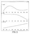
Figure 5 shows the simulation results achieved by the circuit of Figure 4. In
particular three curves are shown, wherein the top curve shows the final
temperature behaviour of the bandgap reference (i.e. Vref), the second curve
shows the current characteristic (INL) of the non-linear circuit 40, and the third
curve shows the voltage generated by the PTAT circuitry (VPTAT). It can be seen
that the non-linear component indicated by the second curve only starts to have
an effect at around 40°C. Also, the top curve Vref shows that the bandgap
reference circuit has a temperature variation of around 1.3 mV over the
temperature range -40 to 120°C compared with a 3 mV variation for a similar
circuit, which does not use the non-linear compensation circuitry.
It should be appreciated that whereas the present application has been described
in relation to bipolar transistors, other transistors for example FET may also be
used. Also, the embodiments described herein are not intended to be limiting
and the npn bipolar transistors can be replaced with pnp transistors and vice
versa if the polarity of the voltage supplies are reversed. Also, although the
device being compensated for is in the preferred embodiment as shown in Figure
4 a bipolar transistor having a negative temperature coefficient across its base-emitter
junction, the present invention is equally applicable to other integrated
circuits that exhibit non-linear temperature characteristics.
Claims (23)
- Reference generating circuitry for generating a reference signal, the circuitry comprising:a first circuit arranged to generate a first signal having a first non-linear temperature characteristic;a second circuit arranged to generate a second a second signal having a second substantially linear temperature characteristic and which partially compensates for the first signal in a first temperature range; anda third circuit arranged to generate a third signal with a third, non-linear temperature characteristic which acts to compensate for the first signal in a second temperature range.
- Reference generating circuitry according to claim 1, wherein the reference signal is a reference voltage, and wherein each of the first, second and third signals are voltages.
- Reference generating circuitry according to claim 1 or 2, wherein the second signal partially compensates for the first signal according to a compensation characteristic, which is modified by the third signal.
- Reference generating circuitry according to claim 3, wherein the compensation characteristic is a bell curve, which is flattened by the third signal.
- Reference generating circuitry for generating a reference signal, the circuitry comprising a first circuit arranged to generate a first signal having a first non-linear temperature characteristic;
a second circuit arranged to generate a second signal having a second substantially linear temperature characteristic and which partially compensates for the first signal according to a compensation characteristic; and
a third circuit arranged to modify the compensation characteristic of the first signal in a non-linear fashion. - The reference generating circuitry of any preceding claim, wherein the first temperature characteristic is a negative temperature coefficient wherein the first signal of the first circuit decreases as temperature increases.
- The reference generating circuitry of any preceding claim, wherein the second temperature characteristic is a positive temperature coefficient wherein the second signal of the second circuit increases as temperature increases.
- The reference generating circuitry of claim 2, wherein the first circuit (Q80) is a first switching device having a control terminal and first and second switching terminals.
- The reference generating circuitry of claim 8, wherein said first switching terminal is connected to the control terminal, and the second switching terminal is connected to a first end of a first resistor (R40) having a second end which is connected to a fourth voltage (GND).
- The reference generating circuitry of claim 9, wherein the reference voltage (Vref) is generated at the first terminal of the first switching device (Q80) and is the voltage (Vbe) across the control and second terminals of the first switching device combined with the voltage (VPTAT) across the first resistor (R40).
- The reference generating circuitry of claim 10, wherein the first terminal of the first switching device (Q80) also being connected to a first terminal of a second switching device (Q70) having a second terminal connected to a fifth voltage (VDD), the second switching device (Q70) having an input to receive an output from the second circuitry (42).
- The reference generating circuitry of claim 11, wherein the output from the second circuitry received at the input of the second switching device is arranged to reflect a current generated from the second circuit (42) through a first branch (203) comprising said second switching device (Q70), the first switching device (Q80) and a first resistor (R40).
- The reference generating circuitry of claim 12, wherein the second circuitry (42) is a proportional to absolute temperature (PTAT) generator comprising a second and a third branch (101, 201), each connected between the fourth (GND) and fifth voltages (VDD).
- The reference generating circuitry of claim 13, wherein the first branch (101) comprises a third and a fourth switching device (Q30, Q40) which share a common switching terminal, and one of the switching terminals of the fourth switching device (Q40) is connected to a first end of a second resistor (R20); and wherein the second branch (201) comprises fifth and sixth switching devices (Q50, Q60) sharing a common switching terminal.
- The reference generating circuitry of claim 14, wherein a control terminal of the third switching device (Q30) is connected to: a control terminal of the fifth switching device (Q50), the common switching terminal between the third and fourth switching devices (Q30, Q40), the control terminal of the second switching device (Q70), and the control terminal of a seventh switching device (Q10) in the third circuit (40).
- The reference generating circuitry of claim 15, wherein a control terminal of the fourth switch device (Q40) is connected to a control terminal of the sixth switching device and the switching terminal common to both the fifth and sixth switching devices (Q50, Q60).
- The reference generating circuitry of claim 16, wherein the other end of the second resistor (R20) is connected to both one end of a third resistor (R30) and a first switching terminal of an eight switching device (Q20), the other end of the resistor and a second switching terminal are both connected to the fourth voltage (GND).
- The reference generating circuitry of claim 17, wherein the third circuitry comprising a fourth branch wherein a first switching terminal of the seventh switching device (Q10) is connected to the fifth voltage (VDD), and a second switching terminal is connected to a first end of a third resistor (R10), the second end is connected to the third voltage, and wherein the first end of the third resistor is connected a control terminal of the eighth switching deice (Q20).
- The reference generating circuitry of any preceding claim, wherein the switching devices are bipolar transistors.
- A method for generating a reference signal, the method comprising:generating a first signal having a first non-linear temperature characteristic;generating a second signal having a second substantially non-linear temperature characteristic which acts to compensate partially for the first signal in a first temperature range; andgenerating a third signal for the third non-linear characteristic which acts to compensate for the first signal in a second temperature range.
- A method for generating a reference signal, the method comprising:generating a first signal having a first non-linear temperature characteristic;generating a second signal having a second substantially linear temperature characteristic which acts to compensate partially for the first signal according to a compensation characteristic; andmodifying the compensation characteristic for the first signal in a non-linear fashion.
- A method according to claim 21, wherein the compensation characteristic is a bell curve which is flattened in the modifying step.
- A method according to claim 20, 21 or 22, wherein the reference signal is a reference voltage.
Priority Applications (2)
| Application Number | Priority Date | Filing Date | Title |
|---|---|---|---|
| EP03256354A EP1522913A1 (en) | 2003-10-09 | 2003-10-09 | Reference circuitry |
| US10/962,371 US20050218967A1 (en) | 2003-10-09 | 2004-10-09 | Reference circuitry and method of operating the same |
Applications Claiming Priority (1)
| Application Number | Priority Date | Filing Date | Title |
|---|---|---|---|
| EP03256354A EP1522913A1 (en) | 2003-10-09 | 2003-10-09 | Reference circuitry |
Publications (1)
| Publication Number | Publication Date |
|---|---|
| EP1522913A1 true EP1522913A1 (en) | 2005-04-13 |
Family
ID=34306999
Family Applications (1)
| Application Number | Title | Priority Date | Filing Date |
|---|---|---|---|
| EP03256354A Withdrawn EP1522913A1 (en) | 2003-10-09 | 2003-10-09 | Reference circuitry |
Country Status (2)
| Country | Link |
|---|---|
| US (1) | US20050218967A1 (en) |
| EP (1) | EP1522913A1 (en) |
Cited By (1)
| Publication number | Priority date | Publication date | Assignee | Title |
|---|---|---|---|---|
| CN115576383A (en) * | 2022-09-20 | 2023-01-06 | 北京聚思芯半导体技术有限公司 | Bandgap reference circuit and bandgap reference chip |
Families Citing this family (1)
| Publication number | Priority date | Publication date | Assignee | Title |
|---|---|---|---|---|
| US11086347B1 (en) * | 2020-02-10 | 2021-08-10 | ZJW Microelectronics Limited | Bandgap reference circuit and electronic device |
Citations (3)
| Publication number | Priority date | Publication date | Assignee | Title |
|---|---|---|---|---|
| US5125112A (en) * | 1990-09-17 | 1992-06-23 | Motorola, Inc. | Temperature compensated current source |
| US5352973A (en) * | 1993-01-13 | 1994-10-04 | Analog Devices, Inc. | Temperature compensation bandgap voltage reference and method |
| US5767664A (en) * | 1996-10-29 | 1998-06-16 | Unitrode Corporation | Bandgap voltage reference based temperature compensation circuit |
Family Cites Families (6)
| Publication number | Priority date | Publication date | Assignee | Title |
|---|---|---|---|---|
| US4939442A (en) * | 1989-03-30 | 1990-07-03 | Texas Instruments Incorporated | Bandgap voltage reference and method with further temperature correction |
| US5952873A (en) * | 1997-04-07 | 1999-09-14 | Texas Instruments Incorporated | Low voltage, current-mode, piecewise-linear curvature corrected bandgap reference |
| US6157245A (en) * | 1999-03-29 | 2000-12-05 | Texas Instruments Incorporated | Exact curvature-correcting method for bandgap circuits |
| US6791307B2 (en) * | 2002-10-04 | 2004-09-14 | Intersil Americas Inc. | Non-linear current generator for high-order temperature-compensated references |
| US6724176B1 (en) * | 2002-10-29 | 2004-04-20 | National Semiconductor Corporation | Low power, low noise band-gap circuit using second order curvature correction |
| US7091713B2 (en) * | 2004-04-30 | 2006-08-15 | Integration Associates Inc. | Method and circuit for generating a higher order compensated bandgap voltage |
-
2003
- 2003-10-09 EP EP03256354A patent/EP1522913A1/en not_active Withdrawn
-
2004
- 2004-10-09 US US10/962,371 patent/US20050218967A1/en not_active Abandoned
Patent Citations (3)
| Publication number | Priority date | Publication date | Assignee | Title |
|---|---|---|---|---|
| US5125112A (en) * | 1990-09-17 | 1992-06-23 | Motorola, Inc. | Temperature compensated current source |
| US5352973A (en) * | 1993-01-13 | 1994-10-04 | Analog Devices, Inc. | Temperature compensation bandgap voltage reference and method |
| US5767664A (en) * | 1996-10-29 | 1998-06-16 | Unitrode Corporation | Bandgap voltage reference based temperature compensation circuit |
Cited By (1)
| Publication number | Priority date | Publication date | Assignee | Title |
|---|---|---|---|---|
| CN115576383A (en) * | 2022-09-20 | 2023-01-06 | 北京聚思芯半导体技术有限公司 | Bandgap reference circuit and bandgap reference chip |
Also Published As
| Publication number | Publication date |
|---|---|
| US20050218967A1 (en) | 2005-10-06 |
Similar Documents
| Publication | Publication Date | Title |
|---|---|---|
| US5900772A (en) | Bandgap reference circuit and method | |
| US6847240B1 (en) | Power-on-reset circuit with temperature compensation | |
| US7259543B2 (en) | Sub-1V bandgap reference circuit | |
| JPH04293275A (en) | Electric current supply provided with adjustable temperature coefficient | |
| US7023181B2 (en) | Constant voltage generator and electronic equipment using the same | |
| KR20040012958A (en) | Proportional to temperature valtage generator | |
| EP2480947A1 (en) | Compensated bandgap | |
| JP2004521540A (en) | Current mirror compensation system for power amplifier | |
| KR101478971B1 (en) | For example, a temperature-compensated current generator for 1-10V interfaces | |
| EP0656574B1 (en) | Voltage reference with linear, negative, temperature coefficient | |
| CN115808950B (en) | Temperature compensation circuit and semiconductor integrated circuit using the same | |
| US7157893B2 (en) | Temperature independent reference voltage generator | |
| US4831323A (en) | Voltage limiting circuit | |
| US6486646B2 (en) | Apparatus for generating constant reference voltage signal regardless of temperature change | |
| JPH10105262A (en) | Voltage controlling means having reduced sensitivity against temperature fluctuation | |
| US20050218967A1 (en) | Reference circuitry and method of operating the same | |
| EP1158382B1 (en) | Generation of a voltage proportional to temperature with stable line voltage | |
| US6650176B1 (en) | N-well resistor leakage cancellation | |
| US6683444B2 (en) | Performance reference voltage generator | |
| JP2003007837A (en) | Reference voltage circuit | |
| US20240143010A1 (en) | Voltage regulator circuit and method for providing a regulated voltage | |
| KR0150196B1 (en) | Bicmos voltage reference generator | |
| US6724598B2 (en) | Solid state switch with temperature compensated current limit | |
| EP1439445A2 (en) | Temperature compensated bandgap voltage reference | |
| KR100571088B1 (en) | Zapping circuit |
Legal Events
| Date | Code | Title | Description |
|---|---|---|---|
| PUAI | Public reference made under article 153(3) epc to a published international application that has entered the european phase |
Free format text: ORIGINAL CODE: 0009012 |
|
| AK | Designated contracting states |
Kind code of ref document: A1 Designated state(s): AT BE BG CH CY CZ DE DK EE ES FI FR GB GR HU IE IT LI LU MC NL PT RO SE SI SK TR |
|
| AX | Request for extension of the european patent |
Extension state: AL LT LV MK |
|
| 17P | Request for examination filed |
Effective date: 20050922 |
|
| AKX | Designation fees paid |
Designated state(s): DE FR GB IT |
|
| 17Q | First examination report despatched |
Effective date: 20060102 |
|
| STAA | Information on the status of an ep patent application or granted ep patent |
Free format text: STATUS: THE APPLICATION IS DEEMED TO BE WITHDRAWN |
|
| 18D | Application deemed to be withdrawn |
Effective date: 20061110 |