EP1521508A1 - Method and apparatus for a unidirectional switching, current limited cutoff circuit for an electronic ballast - Google Patents
Method and apparatus for a unidirectional switching, current limited cutoff circuit for an electronic ballast Download PDFInfo
- Publication number
- EP1521508A1 EP1521508A1 EP04255956A EP04255956A EP1521508A1 EP 1521508 A1 EP1521508 A1 EP 1521508A1 EP 04255956 A EP04255956 A EP 04255956A EP 04255956 A EP04255956 A EP 04255956A EP 1521508 A1 EP1521508 A1 EP 1521508A1
- Authority
- EP
- European Patent Office
- Prior art keywords
- lamp
- inverter circuit
- bus voltage
- voltage
- circuit
- Prior art date
- Legal status (The legal status is an assumption and is not a legal conclusion. Google has not performed a legal analysis and makes no representation as to the accuracy of the status listed.)
- Ceased
Links
- 238000000034 method Methods 0.000 title abstract description 12
- 230000005669 field effect Effects 0.000 claims description 2
- 238000001514 detection method Methods 0.000 claims 1
- 230000000415 inactivating effect Effects 0.000 abstract description 2
- 238000004804 winding Methods 0.000 description 52
- 239000003990 capacitor Substances 0.000 description 49
- 230000001939 inductive effect Effects 0.000 description 10
- 238000010438 heat treatment Methods 0.000 description 6
- 230000015556 catabolic process Effects 0.000 description 5
- 238000010304 firing Methods 0.000 description 5
- 230000010355 oscillation Effects 0.000 description 5
- 230000008878 coupling Effects 0.000 description 4
- 238000010168 coupling process Methods 0.000 description 4
- 238000005859 coupling reaction Methods 0.000 description 4
- 230000007704 transition Effects 0.000 description 3
- 238000006842 Henry reaction Methods 0.000 description 2
- 238000010586 diagram Methods 0.000 description 2
- 238000002955 isolation Methods 0.000 description 2
- 230000009471 action Effects 0.000 description 1
- 230000000903 blocking effect Effects 0.000 description 1
- 230000008859 change Effects 0.000 description 1
- 230000006378 damage Effects 0.000 description 1
- 230000009977 dual effect Effects 0.000 description 1
- 230000000694 effects Effects 0.000 description 1
- 239000000463 material Substances 0.000 description 1
- 230000003071 parasitic effect Effects 0.000 description 1
- 230000002441 reversible effect Effects 0.000 description 1
- 230000000630 rising effect Effects 0.000 description 1
- 238000004544 sputter deposition Methods 0.000 description 1
- 230000036962 time dependent Effects 0.000 description 1
- 230000001052 transient effect Effects 0.000 description 1
- 230000001960 triggered effect Effects 0.000 description 1
Images


Classifications
-
- H—ELECTRICITY
- H05—ELECTRIC TECHNIQUES NOT OTHERWISE PROVIDED FOR
- H05B—ELECTRIC HEATING; ELECTRIC LIGHT SOURCES NOT OTHERWISE PROVIDED FOR; CIRCUIT ARRANGEMENTS FOR ELECTRIC LIGHT SOURCES, IN GENERAL
- H05B41/00—Circuit arrangements or apparatus for igniting or operating discharge lamps
- H05B41/14—Circuit arrangements
- H05B41/26—Circuit arrangements in which the lamp is fed by power derived from DC by means of a converter, e.g. by high-voltage DC
- H05B41/28—Circuit arrangements in which the lamp is fed by power derived from DC by means of a converter, e.g. by high-voltage DC using static converters
- H05B41/295—Circuit arrangements in which the lamp is fed by power derived from DC by means of a converter, e.g. by high-voltage DC using static converters with semiconductor devices and specially adapted for lamps with preheating electrodes, e.g. for fluorescent lamps
-
- H—ELECTRICITY
- H05—ELECTRIC TECHNIQUES NOT OTHERWISE PROVIDED FOR
- H05B—ELECTRIC HEATING; ELECTRIC LIGHT SOURCES NOT OTHERWISE PROVIDED FOR; CIRCUIT ARRANGEMENTS FOR ELECTRIC LIGHT SOURCES, IN GENERAL
- H05B41/00—Circuit arrangements or apparatus for igniting or operating discharge lamps
- H05B41/14—Circuit arrangements
- H05B41/46—Circuits providing for substitution in case of failure of the lamp
Definitions
- the present application relates to ballasts, or power supply circuits for gas discharge lamps. It finds particular application for use with current fed instant and/or rapid start electronic ballasts or power supply circuits and will be described with particular reference thereto. It is to be appreciated, however, that the present application is also applicable to other controllers, and is not limited to the aforementioned use.
- the cathodes are pre-heated with a separate voltage on the cathodes, while maintaining low voltage across the lamp. Therefore, the glow discharge current is low, being less than about 10 ma in comparison with instant start circuits.
- the time that high voltage potentials across the lamp are applied without the lamp conducting is significantly reduced during start-up, and the bombardment of the cathodes does not occur to the same extent as with the instant start method, significantly extending lamp life.
- a lamp inverter circuit includes a switching portion that converts a bus voltage signal into an alternating current signal.
- An input portion receives the bus voltage signal, and a resonant load portion drives a lamp.
- a preheating portion heats the lamp prior to ignition, and thereafter renders itself inactive following ignition of the lamp.
- a method of starting a lamp includes receiving a bus voltage signal, converting the bus voltage signal into an alternating current signal, preheating the lamp to an ignition temperature, igniting the lamp and inactivating the preheating after the lamp has been ignited.
- a method of igniting an auxiliary lamp including detecting a conductive state of a main lamp in a lamp ballast circuit, the detecting being by a switch that controls preheating of the main lamp. The integrity of the main lamp is detected, and current flow is switched from the main lamp to an auxiliary lamp in the event of a main lamp failure.
- lamp circuit A includes a high frequency inverter 10, and a lamp assembly 12.
- Inverter 10 is supplied with a bus voltage 11, and can be either of a current fed or a voltage fed type of high frequency inverters. Both types of inverters utilize inductive circuitry, whether they be inductors or transformers. Tapped off of a portion of the inductive circuitry of inverter 10, are additional inductive winding of winding arrangement 14 that supply power to a unidirectional timing switch circuit 16. These windings supply power that will be used to pre-heat cathodes of lamp assembly 12. Two windings are used for each lamp, as each lamp has two cathodes to pre-heat. For a three lamp configuration, only four to six windings from inductive winding arrangement 14 are tapped off of inverter 10, since one cathode of the three lamps is in parallel and heated by a single winding
- Timing switch circuit 16 is selected to be unidirectional to avoid having to convert an AC control signal into a pulsating DC signal before being controlled by switch circuit 16. This makes for a simpler, lower cost switch arrangement, and aids in allowing the provision of power to the cathodes by a single switch.
- the single switch of timing switch circuit 16 is selected to have a zero voltage turn-on point and a zero current turn-off point. This allows the switch to turn on without excessively high voltages. Otherwise, larger, more expensive switches would be needed to do the same job. Also, utilizing zero voltage turn-on and zero current turn-off minimizes power dissipation when the switch is activated or deactivated. Inverter 10 and timing switch circuit 16 are both gated by a current limiting transformer arrangement 18 that regulates the start-up and currents supplied to lamp cathode assembly 12.
- lamp circuit A including, inverter starting circuit 10 in a current fed half bridge inverter implementation, in operation with a cathode cut-off circuit, comprised of inductive winding arrangement 14, unidirectional timing switch circuit 16, and current limiting transformer arrangement 18.
- a first transistor 20 and a second transistor 22 alternate between periods of conductivity and periods of non-conductivity, out of phase with each other. That is, when the first transistor 20 is conductive, the second transistor 22 is non-conductive, and vice-versa.
- the transistors 20, 22 are part of a switching portion of the inverter circuit 10. The action of alternating periods of conduction of the transistors provides an AC signal to the lamp assembly 12.
- the transistors are bipolar junction transistors (BJTs), but it is to be understood the concepts of the present application may be incorporated in other switching networks, such as known in the art. For example, the following descriptions may be implemented with field effect transistors in both half-bridge current fed ballasts and push-pull type current fed electronic ballasts, among others.
- each transistor 20, 22 has a respective base, (B) emitter, (E) and collector (C).
- the voltage from base r to emitter on either transistor defines the conduction state of that transistor. That is, the base-to-emitter voltage of transistor 20 defines the conductivity of transistor 20 and the base-to-emitter voltage of transistor 22 defines the conductivity of transistor 22.
- neither of the transistors 20, 22 are conductive when current is initially supplied to the inverter starting circuit 10.
- a start-up portion 24 of the inverter circuit prevents current from being supplied to the transistors 20, 22 before the bus voltage reaches a predetermined threshold voltage.
- the start-up portion includes Zener diode 26, diode 28, capacitor 30, and diac 32.
- capacitors 34 and 36 are equivalent to the bus voltage.
- capacitors 34 and 36 are of equal value, so that the voltage across capacitor 34 is the same as the voltage across capacitor 36.
- resistors 38, 40, and 42 are resistors 38, 40, and 42. Resistors 38 and 40 form a voltage divider at node 44 and current is supplied to the start-up portion 24 through voltage divider 38, 40.
- Zener diode 26 and diode 28 prevent any significant current from passing through start-up portion 24.
- a portion of the circuit current charges capacitors 34 and 36, other current charges resonant capacitor 46, and the remaining current flows through resistors 38, 40, and 42.
- resistors 38 and 40 Initially, because half the bus voltage is divided by resistors 38 and 40, a breakdown voltage of Zener diode 26 is not reached, and Zener diode 26 prevents current from passing through start-up portion 24.
- the bus voltage ramps to a level where the potential at node 44 is greater than the breakdown voltage of Zener diode 26 turning Zener diode 26 conductive, supplying increased current levels to start-up portion 24, and more specifically, to capacitor 30.
- the breakdown voltage of Zener diode 26 is between about 60 to 80 V, and preferably 8V.
- Zener diode 26 turns conductive (from left to right in FIG. 2) capacitor 30 begins charging. At this point, current is being supplied to start-up portion 24, but diac 32 prevents the base of transistor 20 from becoming conductive in the collector-emitter direction. As the bus voltage continues ramping up, capacitor 30 collects more charge, and eventually reaches a potential to overcome the breakover voltage of diac 32. When the breakover voltage is reached, transistor 20 turns conductive, wherein inverter starting circuit 12 begins to oscillate, and cathodes of lamp assembly 12 are preheated.
- capacitor 30 no longer has an opportunity to continuously collect charge. Current flows directly from node 44 to the collector of transistor 20, since transistor 20 is conductive after diac 32 breaks down. Diode 28 provides a path to allow capacitor 30 to discharge, once per cycle.
- the inverter starting circuit 10 now operates as is typical, with no further activity from the start-up portion 24.
- switching transistors 20, 22 are driven by respective drive circuits 48, 50.
- Drive circuit 48 incorporates diode 52, resistor 54 combination supplied via coupling of windings 56, 68.
- Drive circuit 50 incorporates diode 60, resistor 62 combination, supplied via coupling of windings 64, 68.
- Lamp assembly 12 is provided with power from inverter circuit 10 by a coupling between windings 68 and 70, where winding 70 has a capacitor 72 across its length and are considered resonant load components. Windings 58 and 66 also serve as current limiting devices.
- power Zener diodes 74 and 76 break down, clamping the voltage across the transistors (e.g., BJTs), to protect them from destruction.
- breakover voltage of diac 32 is chosen to be proportional to an optimal ignition voltage of lamp assembly 12.
- the breakover voltage of diac 32 is chosen to be such that when the bus voltage (the voltage across capacitors 34 and 36) reaches a predetermined value, for example about 390 V, diac 32 reaches its breakover voltage.
- start-up portion 24 detects when the bus voltage reaches the preferred firing voltage by virtue of the chosen breakover voltage of Zener diode 26 and diac 32.
- the breakover voltage of the diac 32 is between 20 V and 40 V, and preferably about 32 V.
- first transistor 20 is also applicable to second transistor 22. That is, in an alternate inverter starting circuit embodiment, the start-up portion 24 is connected to second transistor 22, and it, instead of first transistor 20, would initiate oscillations.
- the preferred firing voltage may be chosen to be less than typical operating voltages for lamps in instant start and rapid start applications, which, in some instances, are approximately 450 V and 500 V, respectively.
- the firing voltage is also chosen to be about 300 V or greater.
- FIGURE 3A provides a graphed time sequence of a rapid start electronic ballast incorporating inverter starting circuit 10 of the present application.
- the sequence includes three distinct transitions. From turn-on (0) to to the bus voltage transitions from its starting voltage (e.g. 169 V) to a preferred pre-heat voltage (e.g. 390 V).
- the time duration to t 0 -t 1 is a pre-heat time (e.g. steady 390 V), and from t 1 to t 2 , the bus voltage ramps up to its steady state (e.g. 500 V).
- FIGURE 3B depicted is a chart showing inverter starting time for a rapid start electronic ballast incorporating inverter starting circuit 10.
- FIGURE 3B illustrates the voltage dependency of the circuit, and emphasizes that operation to start the circuit is not a time dependent factor but is rather a voltage controlled concept. There is no pre-determined time following energization that the oscillations will begin. Rather, in the present design, following energization of the circuit, as long as the bus voltage is below a certain value (e.g. 300 V) there will, ideally, be no oscillations and only when the voltage is at or above the breakover voltage (e.g. 300 V) will the oscillations begin. Thus it is shown the starting of the circuit is controlled by the value of the bus voltage.
- a certain value e.g. 300 V
- FIGURE 4 depicted is operation of charge capacitor 30 of FIGURE 2, which illustrates its two distinct charging rates.
- Charge capacitor 30 will always have an amount of stored energy to be used for the breakover of diac 32.
- capacitor 30 charges at a very quick rate, and when below 300 V bus voltage, capacitor 30 is being charged only due to leakage current.
- Zener diode 26 never turns conductive in its reverse direction, and allows only a leakage current 73a to charge capacitor 30. After the bus voltage reaches 300 V, a significantly higher charging current 73b is available to capacitor 30.
- the threshold voltage is the starting bus voltage. For a 120 V line input, the output bus voltage ramps up from about 169 V. For a 277 V line input, the output bus voltage ramps up from about 390 V. As stated earlier, the start time (FIGURE 3B) is about 40 milliseconds at 390 V. After inverter circuit is oscillating, the bus voltage continues to ramp up to steady state operating voltage V. Thus, one exemplary firing voltage is 390 V, because it is greater than the 300 V required for mode transition, is less than common steady state operating voltages, and triggers the inverter circuit as soon as possible, before the bus voltage reaches steady state. Of course, greater or lesser firing voltages can be chosen, based on known line voltages and desired universality of the inverter.
- Secondary inductive winding 80 of winding arrangement 14 steps up the voltage to and provides isolation for switch circuit 16.
- Resonant winding 70 includes a gap with a relatively low magnetizing inductor. That inductor acts as a resonant component, resonating with capacitors 72 and 46 before the lamp starts. Additionally, capacitors 75, 77, and 78 reflected back to the primary side 70 after lamps of lamp assembly 12 are ignited. Winding 70 combined with capacitors 46, 72, 75, 77, and 78 determine one or multiple operating frequencies of the assembly A.
- Inductor winding 80 is also tapped off of resonant inductor winding 70.
- Winding 80 supplies power to switching circuit primary winding 82.
- Winding 82 in turn supplies power to cathode windings 84, 86, 88, and 90.
- Cathode windings 84, 86, 88, and 90 pre-heat the cathodes of the lamps of lamp assembly 12. It is to be understood that cathode windings 84; 86, 88, and 90 act as the secondary of the primary winding 82.
- the primary winding has a higher number of turns and thus, a lower current is needed in the primary winding 82. Otherwise, costlier devices would be called for switching device 94 that can accommodate higher currents.
- Capacitor 92 limits the current that winding 80 supplies to primary winding 82. If the value of capacitor 92 is chosen to be sufficiently low, it limits the maximum current supplied to winding 82. Capacitor 92 serves a dual purpose; it acts as a DC blocking cap when transistor 94 is inactive. After a few cycles, this removes winding 82 from the circuit. That is, when transistor 94 goes inactive, no heating is being supplied to the cathodes. Diode 96 is connected back between capacitors 34 and 36 and protects transistor 94 from being supplied with excess voltage when transistor 94 goes inactive, during its transient state.
- Winding arrangement 14 of FIGURE 1 also includes an inductor winding 98, which supplies current through diode 100 and charges capacitor 102.
- Capacitor 102 is subject to the RC time constant defined by capacitor 106 and resistor 104. The time constant is selected to remove heating from the cathodes a safe time after lamp assembly 12 ignites, for example, it may be several seconds to 10 seconds or more after the inverter circuit is ignited.
- Capacitor 102 is connected to the gate of FET 108 via resistor 104.
- the RC time constant defined by capacitor 106 and resistor 104 When the RC time constant defined by capacitor 106 and resistor 104 is fulfilled, charge developed on capacitor 102 causes FET 108 to become conductive. The gate of FET 94 is then brought down to a lower voltage level, causing FET 94 to become inactive. As stated previously, when FET 94 turns inactive, the voltage on the cathodes switch of circuit 16 is removed, thereby removing heating to the cathodes.
- Transistors 94 and 108 are depicted as MOSFETs, but it is to be understood that a similar circuit architecture could be accomplished using bipolar junction transistors or other switching devices.
- FIGURE 5 depicted is an alternate cathode cut-off circuit 14', 16', 18' embodiment with a portion of a half bridge voltage fed rapid start electronic inverter 10'.
- the inverter 10' uses FET switches 20', 22'.
- This design incorporates an additional winding 110 tapped to resonant inductor 112.
- Power to the cathodes 114, 116 is derived from winding 110 on the resonant inductor 112 via capacitor 92 and primary winding 82 elements with similar functions to those in FIGURE 2 are numbered similar to those in
- FIGURE 2 is a diagrammatic representation of FIGURE 1
- FIGURES 2 and 5 are two implementations of a new starting circuit in conjunction with current or voltage fed, half-bridge inverter circuits, which also implements a cathode cut-off circuit, which employs a unidirectional switching current design.
- the main bus voltage may be sensed by a three resistor divider circuit. A portion of the bus voltage is applied to a Zener diode and a charging capacitor. When the voltage reaches a predetermined level, the Zener diode breaks down, allowing the charging capacitor to 10 charge. A diac then breaks down, causing the self-oscillating inverter to be triggered.
- a diode prevents the charging capacitor from charging, allowing it to discharge every half-cycle, when a first transistor is on.
- the component values are selected such that the Zener breakdown voltage is at least double the diac breakdown voltage, or higher.
- the unidirectional switch circuit controls the energy delivered to the lamp cathodes, and current limiting capacitor prevents current from rising to dangerous levels. This protects the arrangement from possible miswirings, such as if one or more cathodes were shorted.
- Single unidirectional transistor switch 94 is turned on with zero voltage prior to oscillations of inverter transistors 20 (20) and 22 (22'), and turns off with zero current when the parasitic antiparallel diode of the FET --- or a diode in parallel with the BJT --- is conducting.
- Transistor 108 controls the removal of cathode heating after the lamp has started and stabilized. Possible applications of the present invention include General Electric's 4 ft. and 8 ft. T12 and T8 electronic lamp ballasts
- the preheating circuit (14, 16, 18) may be used to provide auxiliary power when the main lamp (e.g., of assembly 12) has failed or is otherwise not in use.
- an auxiliary lamp 120 may be connected to the preheat circuit (14, 16, 18).
- the auxiliary lamp may be a low-power fluorescent lamp, incandescent lamp or other lighting element. Therefore, in place of the additional windings 14, 18 being used to pre-heat the cathodes of lamp assembly 12, they are connected to the auxiliary lamp 120.
- This connection may be accomplished by the coupling of windings in a manner as discussed in connection with FIGURES 2 and 5 (e.g., winding 82), to provide power and control for the auxiliary lamp 120 or use a independent inverter circuit to power and control the auxiliary lamp.
- This design provides a very low cost control to the auxiliary lighting in part due to the use of a single switch (e.g., 94) control, in place of a two-switch system.
- the auxiliary lighting may be applicable 11 in a variety of situations such as back-up lighting and emergency lighting situations.
- the preheating circuit (14, 16, 18) may be used to deliver power to an auxiliary lamp 120.
- Some exemplary component values for the circuits of FIGURES 2 and 5 are as follows: Part Description Nominal Value Nominal Value Lamp Assembly 10 40 Watts Line Voltage 11 120-277 Volts First Transistor 20 BJT SPB 11 NM60 Second Transistor 22 BJT SPB 11 NM60 Bus Capacitor 34 33 ⁇ f Bus Capacitor 36 33 ⁇ f Bus Resistor 38 400 k ⁇ Bus Resistor 40 620 k ⁇ Bus Resistor 42 1 M ⁇ Diode 28 UF 4007 Capacitor 46 1.2 nf Charging Capacitor 30 0.1 ⁇ f Diac 32 HT-32 Zener Diode 76 P6KE440A Base Diode 52 1N5817 Base Diode 60 1N5817 Base Resistor 54 75 ⁇ Base Resistor 62 75 ⁇ Inductive Winding 58 5m Henries Inductive Winding 66 5m Henries Inductive Winding 70 0.85mH Inductive Winding 68 1.27mH Capacitor 72 0.01u
Landscapes
- Circuit Arrangements For Discharge Lamps (AREA)
Abstract
Description
- The present application relates to ballasts, or power supply circuits for gas discharge lamps. It finds particular application for use with current fed instant and/or rapid start electronic ballasts or power supply circuits and will be described with particular reference thereto. It is to be appreciated, however, that the present application is also applicable to other controllers, and is not limited to the aforementioned use.
- Presently there are two prevailing starting methods for starting gas discharge lamps. One is instant start, and the other is rapid start. In both the instant start and rapid start methods, cathodes of the lamp are pre-heated before lamp ignition. With an instant start electronic ballast, the cathodes are preheated by a glow discharge current. This is the current that goes through the lamp before the lamp ignites. Typically, the voltage potential of the glow discharge current is high, and can range between approximately 400 and 500 Vrms or more. In the preheating phase, when the lamp is not conducting, such high potential differences can cause bombardment of the cathodes, resulting in some of the physical material of the cathode sputtering off each time the lamp is lit. Thus, lamps that utilize the instant start method of ignition tend not to have as long lives as lamps that utilize the rapid start method. Typically, a lamp that uses instant start will last about 80% as long as the same type of lamp using rapid start.
- With a rapid start electronic ballast, the cathodes are pre-heated with a separate voltage on the cathodes, while maintaining low voltage across the lamp. Therefore, the glow discharge current is low, being less than about 10 ma in comparison with instant start circuits. In the rapid start mode, the time that high voltage potentials across the lamp are applied without the lamp conducting is significantly reduced during start-up, and the bombardment of the cathodes does not occur to the same extent as with the instant start method, significantly extending lamp life.
- There is a drawback, however, to using the rapid start mode. Presently, once a preheating current is applied, it is generally not removed from the cathodes, even after the lamp ignites. Resultantly, while the lamp is lit, the low voltage heating current is continuously applied on the cathodes. Thus, lamps that utilize the rapid start method to start are consuming more power than lamps that use the instant start method. With a single lamp, it is likely that up to about 1.5 extra Watts of power will be consumed, and with a three lamp ballast, it is likely that between 4.5 and 6 extra Watts of power will be consumed. This extra power is consumed (simply producing heat) without producing any added light output, that is, without producing extra lumens. Thus, the trade-off from instant start to rapid start is greater lamp life for added power consumption.
- In accordance with one aspect of the present application, a lamp inverter circuit includes a switching portion that converts a bus voltage signal into an alternating current signal. An input portion receives the bus voltage signal, and a resonant load portion drives a lamp. A preheating portion heats the lamp prior to ignition, and thereafter renders itself inactive following ignition of the lamp.
- In accordance with another aspect of the present application, a method of starting a lamp includes receiving a bus voltage signal, converting the bus voltage signal into an alternating current signal, preheating the lamp to an ignition temperature, igniting the lamp and inactivating the preheating after the lamp has been ignited.
- In accordance with another aspect of the application, provided is a method of igniting an auxiliary lamp, including detecting a conductive state of a main lamp in a lamp ballast circuit, the detecting being by a switch that controls preheating of the main lamp. The integrity of the main lamp is detected, and current flow is switched from the main lamp to an auxiliary lamp in the event of a main lamp failure.
- The invention will now be described in greater detail, by way of example, with reference to the drawings, in which:-
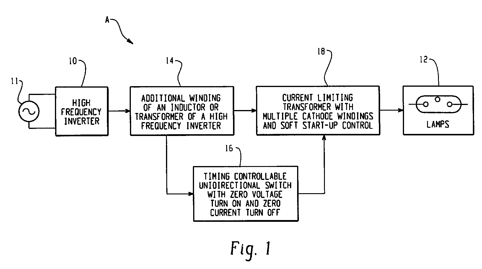
- FIGURE 1 is a block diagram of a lamp system in accordance with the present application;
- FIGURE 2 is a circuit diagram of a ballast inverter circuit included in the lamp system shown in FIGURE 1, in accordance with one aspect of the present application;
- FIGURE 3A shows the bus voltage over a time sequence for the rapid start electronic ballast according to the present application;
- FIGURE 3B provides a function of the bus voltage versus starting time for a rapid start electronic ballast according to the present application;
- FIGURE 4 depicts the charge current of
capacitor 30 of FIGURE 2 as a function of the bus voltage; - FIGURE 5 shows an alternate architecture of a portion of the circuit of FIGURE 2, with an additional winding tapped into the resonant inductor.
-
- With reference to FIGURE 1, lamp circuit A includes a
high frequency inverter 10, and alamp assembly 12.Inverter 10 is supplied with abus voltage 11, and can be either of a current fed or a voltage fed type of high frequency inverters. Both types of inverters utilize inductive circuitry, whether they be inductors or transformers. Tapped off of a portion of the inductive circuitry ofinverter 10, are additional inductive winding ofwinding arrangement 14 that supply power to a unidirectionaltiming switch circuit 16. These windings supply power that will be used to pre-heat cathodes oflamp assembly 12. Two windings are used for each lamp, as each lamp has two cathodes to pre-heat. For a three lamp configuration, only four to six windings frominductive winding arrangement 14 are tapped off ofinverter 10, since one cathode of the three lamps is in parallel and heated by a single winding -
Timing switch circuit 16 is selected to be unidirectional to avoid having to convert an AC control signal into a pulsating DC signal before being controlled byswitch circuit 16. This makes for a simpler, lower cost switch arrangement, and aids in allowing the provision of power to the cathodes by a single switch. The single switch oftiming switch circuit 16 is selected to have a zero voltage turn-on point and a zero current turn-off point. This allows the switch to turn on without excessively high voltages. Otherwise, larger, more expensive switches would be needed to do the same job. Also, utilizing zero voltage turn-on and zero current turn-off minimizes power dissipation when the switch is activated or deactivated.Inverter 10 andtiming switch circuit 16 are both gated by a current limitingtransformer arrangement 18 that regulates the start-up and currents supplied tolamp cathode assembly 12. - With reference to FIGURE 2, illustrated is a more detailed view of the lamp circuit A including,
inverter starting circuit 10 in a current fed half bridge inverter implementation, in operation with a cathode cut-off circuit, comprised ofinductive winding arrangement 14, unidirectionaltiming switch circuit 16, and current limitingtransformer arrangement 18. - In order to convert a DC bus signal into an AC signal, a
first transistor 20 and asecond transistor 22 alternate between periods of conductivity and periods of non-conductivity, out of phase with each other. That is, when thefirst transistor 20 is conductive, thesecond transistor 22 is non-conductive, and vice-versa. Thetransistors inverter circuit 10. The action of alternating periods of conduction of the transistors provides an AC signal to thelamp assembly 12. In the embodiment illustrated in FIGURE 2, the transistors are bipolar junction transistors (BJTs), but it is to be understood the concepts of the present application may be incorporated in other switching networks, such as known in the art. For example, the following descriptions may be implemented with field effect transistors in both half-bridge current fed ballasts and push-pull type current fed electronic ballasts, among others. - In this embodiment, each
transistor transistor 20 defines the conductivity oftransistor 20 and the base-to-emitter voltage oftransistor 22 defines the conductivity oftransistor 22. In the illustrated embodiment neither of thetransistors inverter starting circuit 10. As will be expanded upon below, a start-up portion 24 of the inverter circuit prevents current from being supplied to thetransistors diode 26,diode 28,capacitor 30, anddiac 32. - The potential difference across
capacitors capacitors capacitor 34 is the same as the voltage acrosscapacitor 36. In parallel withcapacitors resistors Resistors node 44 and current is supplied to the start-upportion 24 throughvoltage divider - When power is first applied to the
inverter starting circuit 10,Zener diode 26 anddiode 28 prevent any significant current from passing through start-upportion 24. As the bus voltage ramps up, after power is initially supplied to inverter startingcircuit 10, a portion of the circuitcurrent charges capacitors resonant capacitor 46, and the remaining current flows throughresistors resistors Zener diode 26 is not reached, andZener diode 26 prevents current from passing through start-upportion 24. Eventually, the bus voltage ramps to a level where the potential atnode 44 is greater than the breakdown voltage ofZener diode 26 turningZener diode 26 conductive, supplying increased current levels to start-upportion 24, and more specifically, tocapacitor 30. In the illustrated embodiment, the breakdown voltage ofZener diode 26 is between about 60 to 80 V, and preferably 8V. - Once
Zener diode 26 turns conductive (from left to right in FIG. 2)capacitor 30 begins charging. At this point, current is being supplied to start-upportion 24, but diac 32 prevents the base oftransistor 20 from becoming conductive in the collector-emitter direction. As the bus voltage continues ramping up,capacitor 30 collects more charge, and eventually reaches a potential to overcome the breakover voltage ofdiac 32. When the breakover voltage is reached,transistor 20 turns conductive, whereininverter starting circuit 12 begins to oscillate, and cathodes oflamp assembly 12 are preheated. - After the breakover voltage of
diac 32 is reached,capacitor 30 no longer has an opportunity to continuously collect charge. Current flows directly fromnode 44 to the collector oftransistor 20, sincetransistor 20 is conductive after diac 32 breaks down.Diode 28 provides a path to allowcapacitor 30 to discharge, once per cycle. Theinverter starting circuit 10 now operates as is typical, with no further activity from the start-upportion 24. - With continuing attention to FIGURE 2, switching
transistors respective drive circuits circuit 48 incorporatesdiode 52,resistor 54 combination supplied via coupling ofwindings circuit 50 incorporatesdiode 60,resistor 62 combination, supplied via coupling ofwindings Lamp assembly 12 is provided with power frominverter circuit 10 by a coupling betweenwindings capacitor 72 across its length and are considered resonant load components.Windings - In the event of sudden load change,
power Zener diodes - With continuing attention to FIGURE 2, breakover voltage of
diac 32 is chosen to be proportional to an optimal ignition voltage oflamp assembly 12. In the illustrated embodiment, the breakover voltage ofdiac 32 is chosen to be such that when the bus voltage (the voltage acrosscapacitors 34 and 36) reaches a predetermined value, for example about 390 V, diac 32 reaches its breakover voltage. Stated differently, start-upportion 24 detects when the bus voltage reaches the preferred firing voltage by virtue of the chosen breakover voltage ofZener diode 26 anddiac 32. In the illustrated embodiment, the breakover voltage of thediac 32 is between 20 V and 40 V, and preferably about 32 V. - It is to be understood the above description that applies to
first transistor 20 is also applicable tosecond transistor 22. That is, in an alternate inverter starting circuit embodiment, the start-upportion 24 is connected tosecond transistor 22, and it, instead offirst transistor 20, would initiate oscillations. - Also, the preferred firing voltage may be chosen to be less than typical operating voltages for lamps in instant start and rapid start applications, which, in some instances, are approximately 450 V and 500 V, respectively. The firing voltage is also chosen to be about 300 V or greater.
- FIGURE 3A provides a graphed time sequence of a rapid start electronic ballast incorporating
inverter starting circuit 10 of the present application. As seen from this figure, the sequence includes three distinct transitions. From turn-on (0) to to the bus voltage transitions from its starting voltage (e.g. 169 V) to a preferred pre-heat voltage (e.g. 390 V). The time duration to t0-t1 is a pre-heat time (e.g. steady 390 V), and from t1 to t2, the bus voltage ramps up to its steady state (e.g. 500 V). Turning attention to FIGURE 3B, depicted is a chart showing inverter starting time for a rapid start electronic ballast incorporatinginverter starting circuit 10. Viewing FIGURES 3A and 3B together emphasizes the starting time is controlled by the bus voltage of the circuit. For example if the bus voltage is less than 300 V, the inverter circuit will take approximately 10 seconds to start, however, when the bus voltage is 300 V or more, the start time is reduced to approximately 40 milliseconds.
FIGURE 3B illustrates the voltage dependency of the circuit, and emphasizes that operation to start the circuit is not a time dependent factor but is rather a voltage controlled concept. There is no pre-determined time following energization that the oscillations will begin. Rather, in the present design, following energization of the circuit, as long as the bus voltage is below a certain value (e.g. 300 V) there will, ideally, be no oscillations and only when the voltage is at or above the breakover voltage (e.g. 300 V) will the oscillations begin. Thus it is shown the starting of the circuit is controlled by the value of the bus voltage. - Turning now to FIGURE 4, depicted is operation of
charge capacitor 30 of FIGURE 2, which illustrates its two distinct charging rates.Charge capacitor 30 will always have an amount of stored energy to be used for the breakover ofdiac 32. As seen, when the bus voltage is over 300 V,capacitor 30 charges at a very quick rate, and when below 300 V bus voltage,capacitor 30 is being charged only due to leakage current. Particularly, when the bus voltage is less than 300 V,Zener diode 26 never turns conductive in its reverse direction, and allows only a leakage current 73a to chargecapacitor 30. After the bus voltage reaches 300 V, a significantly higher charging current 73b is available tocapacitor 30. - Another consideration in selecting the threshold voltage is the starting bus voltage. For a 120 V line input, the output bus voltage ramps up from about 169 V. For a 277 V line input, the output bus voltage ramps up from about 390 V. As stated earlier, the start time (FIGURE 3B) is about 40 milliseconds at 390 V. After inverter circuit is oscillating, the bus voltage continues to ramp up to steady state operating voltage V. Thus, one exemplary firing voltage is 390 V, because it is greater than the 300 V required for mode transition, is less than common steady state operating voltages, and triggers the inverter circuit as soon as possible, before the bus voltage reaches steady state. Of course, greater or lesser firing voltages can be chosen, based on known line voltages and desired universality of the inverter.
- Returning to FIGURE 2, attention is now drawn to the cathode cutoff or preheat control circuit (14, 16, 18). In this design, winding 70 and 68--- in addition to being designed for resonant inductance --- also provides isolation to the ballast. Secondary inductive winding 80 of winding
arrangement 14 steps up the voltage to and provides isolation forswitch circuit 16. Resonant winding 70 includes a gap with a relatively low magnetizing inductor. That inductor acts as a resonant component, resonating withcapacitors capacitors primary side 70 after lamps oflamp assembly 12 are ignited. Winding 70 combined withcapacitors - Inductor winding 80 is also tapped off of resonant inductor winding 70. Winding 80 supplies power to switching circuit primary winding 82. Winding 82 in turn supplies power to
cathode windings Cathode windings lamp assembly 12. It is to be understood thatcathode windings 84; 86, 88, and 90 act as the secondary of the primary winding 82. The primary winding has a higher number of turns and thus, a lower current is needed in the primary winding 82. Otherwise, costlier devices would be called for switchingdevice 94 that can accommodate higher currents. Lower current devices are also desired to reduce power dissipation.Capacitor 92 limits the current that winding 80 supplies to primary winding 82. If the value ofcapacitor 92 is chosen to be sufficiently low, it limits the maximum current supplied to winding 82.Capacitor 92 serves a dual purpose; it acts as a DC blocking cap whentransistor 94 is inactive. After a few cycles, this removes winding 82 from the circuit. That is, whentransistor 94 goes inactive, no heating is being supplied to the cathodes.Diode 96 is connected back betweencapacitors transistor 94 from being supplied with excess voltage whentransistor 94 goes inactive, during its transient state. - Winding
arrangement 14 of FIGURE 1 also includes an inductor winding 98, which supplies current throughdiode 100 and charges capacitor 102.Capacitor 102 is subject to the RC time constant defined bycapacitor 106 andresistor 104. The time constant is selected to remove heating from the cathodes a safe time afterlamp assembly 12 ignites, for example, it may be several seconds to 10 seconds or more after the inverter circuit is ignited.Capacitor 102 is connected to the gate ofFET 108 viaresistor 104. When the RC time constant defined bycapacitor 106 andresistor 104 is fulfilled, charge developed oncapacitor 102causes FET 108 to become conductive. The gate ofFET 94 is then brought down to a lower voltage level, causingFET 94 to become inactive. As stated previously, whenFET 94 turns inactive, the voltage on the cathodes switch ofcircuit 16 is removed, thereby removing heating to the cathodes. -
Transistors - Turning to FIGURE 5, depicted is an alternate cathode cut-off circuit 14', 16', 18' embodiment with a portion of a half bridge voltage fed rapid start
electronic inverter 10'. Theinverter 10' uses FET switches 20', 22'. This design incorporates an additional winding 110 tapped toresonant inductor 112. Power to thecathodes resonant inductor 112 viacapacitor 92 and primary winding 82 elements with similar functions to those in FIGURE 2 are numbered similar to those in - Thus, from the foregoing, it is shown (FIGURES 2 and 5) are two implementations of a new starting circuit in conjunction with current or voltage fed, half-bridge inverter circuits, which also implements a cathode cut-off circuit, which employs a unidirectional switching current design. The main bus voltage may be sensed by a three resistor divider circuit. A portion of the bus voltage is applied to a Zener diode and a charging capacitor. When the voltage reaches a predetermined level, the Zener diode breaks down, allowing the charging capacitor to 10 charge. A diac then breaks down, causing the self-oscillating inverter to be triggered. A diode prevents the charging capacitor from charging, allowing it to discharge every half-cycle, when a first transistor is on. The component values are selected such that the Zener breakdown voltage is at least double the diac breakdown voltage, or higher. The unidirectional switch circuit controls the energy delivered to the lamp cathodes, and current limiting capacitor prevents current from rising to dangerous levels. This protects the arrangement from possible miswirings, such as if one or more cathodes were shorted. Single
unidirectional transistor switch 94 is turned on with zero voltage prior to oscillations of inverter transistors 20 (20) and 22 (22'), and turns off with zero current when the parasitic antiparallel diode of the FET --- or a diode in parallel with the BJT --- is conducting.Transistor 108 controls the removal of cathode heating after the lamp has started and stabilized. Possible applications of the present invention include General Electric's 4 ft. and 8 ft. T12 and T8 electronic lamp ballasts. - Additional embodiments of the described designs may be found in starting auxiliary power circuits when a main lamp is down. For example, with reference to FIGURE I, as shown by the dotted lines, the preheating circuit (14, 16, 18) may be used to provide auxiliary power when the main lamp (e.g., of assembly 12) has failed or is otherwise not in use. In this situation, an auxiliary lamp 120 may be connected to the preheat circuit (14, 16, 18). The auxiliary lamp may be a low-power fluorescent lamp, incandescent lamp or other lighting element. Therefore, in place of the
additional windings lamp assembly 12, they are connected to the auxiliary lamp 120. This connection may be accomplished by the coupling of windings in a manner as discussed in connection with FIGURES 2 and 5 (e.g., winding 82), to provide power and control for the auxiliary lamp 120 or use a independent inverter circuit to power and control the auxiliary lamp. This design provides a very low cost control to the auxiliary lighting in part due to the use of a single switch (e.g., 94) control, in place of a two-switch system. The auxiliary lighting may be applicable 11 in a variety of situations such as back-up lighting and emergency lighting situations. Thus, instead of heating a cathode, the preheating circuit (14, 16, 18) may be used to deliver power to an auxiliary lamp 120. - Some exemplary component values for the circuits of FIGURES 2 and 5 are as follows:
Part Description Nominal Value Nominal Value Lamp Assembly 10 40 Watts Line Voltage 11 120-277 Volts First Transistor 20 BJT SPB 11NM60 Second Transistor 22 BJT SPB 11NM60 Bus Capacitor 34 33 µf Bus Capacitor 36 33 µf Bus Resistor 38 400 kΩ Bus Resistor 40 620 kΩ Bus Resistor 42 1 MΩ Diode 28 UF 4007 Capacitor 46 1.2 nf Charging Capacitor 30 0.1 µf Diac 32 HT-32 Zener Diode 76 P6KE440A Base Diode 52 1N5817 Base Diode 60 1N5817 Base Resistor 54 75 Ω Base Resistor 62 75 Ω Inductive Winding 58 5m Henries Inductive Winding 66 5m Henries Inductive Winding 70 0.85mH Inductive Winding 68 1.27mH Capacitor 72 0.01 uf Zener Diode 74 P6KE440A Capacitor 75 0.0056 uf Zener Diode 26 68 V Capacitor 77 0.0056 uf Capacitor 78 0.0056 uf Winding 80 0.47mh Primary Cathode Winding 82 1mh Secondary Cathode Winding 84 2uh Secondary Cathode Winding 86 2uh Secondary Cathode Winding 88 2uh Secondary Cathode Winding 90 2uh Capacitor 92 4.7nf - It is to be understood that the foregoing components and values may be altered depending on the specific implementation, and values not listed may be selected in accordance with such implementations.
Claims (10)
- A lamp inverter circuit (10) comprising:a switching portion (20, 22) that converts a bus voltage signal into an alternatingcurrent signal;an input portion that receives the bus voltage signal;a resonant load portion (70, 72) for driving a lamp (12); and,a preheating portion (16) that:heats the lamp (12) prior to ignition of the lamp (12); and,renders itself inactive after ignition of the lamp(12).
- The lamp inverter circuit (10) as set forth in claim 1, wherein the cathode preheating portion (16) includes an unidirectional switch (94) used to control energy delivered to the at least one lamp (12).
- The lamp inverter circuit (10) as set forth in claim 2, wherein the inverter circuit is one of a voltage fed or current fed circuit.
- The lamp inverter circuit (10) as set forth in claim 2, wherein the unidirectional switch (94) is a field effect transistor.
- The lamp inverter circuit (10) as set forth in claim 2, wherein the unidirectional switch (94) is a bipolar junction transistor.
- The lamp inverter circuit (10) as set forth in claim 2, wherein the unidirectional switch (94) detects if one of the lamp (12) and the bus voltage signal has failed.
- The lamp inverter circuit (10) as set forth in claim 6, wherein the unidirectional switch (94) ignites an auxiliary light source upon detection of failure of one of the bus voltage and the lamp (12).
- The lamp inverter circuit (10) as set forth in claim 6, further including a current limiting device (92) to limit a maximum current, upon failure of the lamp (12).
- The lamp inverter circuit (10) as set forth in claim 2, wherein the unidirectional switch (94) has a zero voltage turn-on point.
- The lamp inverter circuit (10) as set forth in claim 2, wherein the unidirectional switch (94) has a zero current turn-off point.
Applications Claiming Priority (2)
| Application Number | Priority Date | Filing Date | Title |
|---|---|---|---|
| US10/675,441 US6936970B2 (en) | 2003-09-30 | 2003-09-30 | Method and apparatus for a unidirectional switching, current limited cutoff circuit for an electronic ballast |
| US675441 | 2003-09-30 |
Publications (1)
| Publication Number | Publication Date |
|---|---|
| EP1521508A1 true EP1521508A1 (en) | 2005-04-06 |
Family
ID=34313988
Family Applications (1)
| Application Number | Title | Priority Date | Filing Date |
|---|---|---|---|
| EP04255956A Ceased EP1521508A1 (en) | 2003-09-30 | 2004-09-29 | Method and apparatus for a unidirectional switching, current limited cutoff circuit for an electronic ballast |
Country Status (3)
| Country | Link |
|---|---|
| US (1) | US6936970B2 (en) |
| EP (1) | EP1521508A1 (en) |
| CN (1) | CN1604716B (en) |
Cited By (2)
| Publication number | Priority date | Publication date | Assignee | Title |
|---|---|---|---|---|
| WO2011020199A1 (en) * | 2009-08-21 | 2011-02-24 | Queen's University At Kingston | Electronic ballast with high power factor |
| US8212492B2 (en) | 2008-06-13 | 2012-07-03 | Queen's University At Kingston | Electronic ballast with high power factor |
Families Citing this family (5)
| Publication number | Priority date | Publication date | Assignee | Title |
|---|---|---|---|---|
| US7420336B2 (en) * | 2004-12-30 | 2008-09-02 | General Electric Company | Method of controlling cathode voltage with low lamp's arc current |
| US7573204B2 (en) * | 2006-12-29 | 2009-08-11 | General Electric Company | Standby lighting for lamp ballasts |
| US7733028B2 (en) * | 2007-11-05 | 2010-06-08 | General Electric Company | Method and system for eliminating DC bias on electrolytic capacitors and shutdown detecting circuit for current fed ballast |
| US7839094B2 (en) * | 2008-05-02 | 2010-11-23 | General Electric Company | Voltage fed programmed start ballast |
| US8922131B1 (en) | 2011-10-10 | 2014-12-30 | Universal Lighting Technologies, Inc. | Series resonant inverter with capacitive power compensation for multiple lamp parallel operation |
Citations (5)
| Publication number | Priority date | Publication date | Assignee | Title |
|---|---|---|---|---|
| US5521467A (en) | 1994-03-25 | 1996-05-28 | Patent-Treuhand-Gesellschaft F. Elektrische Gluehlampen Mbh | High power factor, high-frequency operating circuit for a low-pressure discharge lamp |
| US5543690A (en) * | 1991-06-21 | 1996-08-06 | Prolux Maschinenbau Gmbh | High voltage ignition circuit for a discharge lamp |
| EP0831678A2 (en) * | 1996-09-19 | 1998-03-25 | General Electric Company | High voltage IC-driven half-bridge gas discharge lamp ballast |
| US5986408A (en) | 1998-04-02 | 1999-11-16 | U.S. Philips Corporation | Discharge lamp with heating electrode circuit |
| US6501225B1 (en) * | 2001-08-06 | 2002-12-31 | Osram Sylvania Inc. | Ballast with efficient filament preheating and lamp fault protection |
Family Cites Families (19)
| Publication number | Priority date | Publication date | Assignee | Title |
|---|---|---|---|---|
| DE3841227A1 (en) | 1988-12-07 | 1990-06-13 | Patent Treuhand Ges Fuer Elektrische Gluehlampen Mbh | CIRCUIT ARRANGEMENT FOR OPERATING A LOW-PRESSURE DISCHARGE LAMP |
| US5796216A (en) | 1993-07-16 | 1998-08-18 | Delta Power Supply, Inc. | Electronic ignition enhancing circuit having both fundamental and harmonic resonant circuits as well as a DC offset |
| JPH07235564A (en) * | 1993-12-27 | 1995-09-05 | Toshiba Corp | Semiconductor device |
| JP3329929B2 (en) * | 1994-02-15 | 2002-09-30 | 松下電工株式会社 | High pressure discharge lamp lighting device |
| US5623187A (en) | 1994-12-28 | 1997-04-22 | Philips Electronics North America Corporation | Controller for a gas discharge lamp with variable inverter frequency and with lamp power and bus voltage control |
| US5569984A (en) | 1994-12-28 | 1996-10-29 | Philips Electronics North America Corporation | Method and controller for detecting arc instabilities in gas discharge lamps |
| US6011362A (en) | 1996-11-19 | 2000-01-04 | Electro-Mag International, Inc. | Magnetic ballast adaptor circuit |
| US5932976A (en) | 1997-01-14 | 1999-08-03 | Matsushita Electric Works R&D Laboratory, Inc. | Discharge lamp driving |
| US6034489A (en) | 1997-12-04 | 2000-03-07 | Matsushita Electric Works R&D Laboratory, Inc. | Electronic ballast circuit |
| JP2002500820A (en) * | 1998-04-02 | 2002-01-08 | コーニンクレッカ フィリップス エレクトロニクス エヌ ヴィ | Circuit layout |
| US6495971B1 (en) | 1998-06-13 | 2002-12-17 | Hatch Transformers, Inc. | High intensity discharge lamp ballast |
| US6184630B1 (en) | 1999-02-08 | 2001-02-06 | Philips Electronics North America Corporation | Electronic lamp ballast with voltage source power feedback to AC-side |
| US6020691A (en) | 1999-04-30 | 2000-02-01 | Matsushita Electric Works R & D Laboratory, Inc. | Driving circuit for high intensity discharge lamp electronic ballast |
| DE19923238A1 (en) | 1999-05-20 | 2001-01-11 | Patent Treuhand Ges Fuer Elektrische Gluehlampen Mbh | Circuit for correcting the power factor |
| US6337800B1 (en) | 2000-02-29 | 2002-01-08 | Philips Electronics North American Corporation | Electronic ballast with inductive power feedback |
| US6483252B2 (en) | 2000-12-08 | 2002-11-19 | Koninklijke Philips Electronics N.V. | Optimal FM for HF operation of high intensity discharge (HID) lamps |
| US6417631B1 (en) | 2001-02-07 | 2002-07-09 | General Electric Company | Integrated bridge inverter circuit for discharge lighting |
| US6803730B2 (en) | 2001-03-21 | 2004-10-12 | International Rectifier Corporation | Single stage PFC + ballast control circuit/general purpose power converter |
| US6593703B2 (en) * | 2001-06-15 | 2003-07-15 | Matsushita Electric Works, Ltd. | Apparatus and method for driving a high intensity discharge lamp |
-
2003
- 2003-09-30 US US10/675,441 patent/US6936970B2/en not_active Expired - Fee Related
-
2004
- 2004-09-29 EP EP04255956A patent/EP1521508A1/en not_active Ceased
- 2004-09-30 CN CN200410085585.8A patent/CN1604716B/en not_active Expired - Fee Related
Patent Citations (5)
| Publication number | Priority date | Publication date | Assignee | Title |
|---|---|---|---|---|
| US5543690A (en) * | 1991-06-21 | 1996-08-06 | Prolux Maschinenbau Gmbh | High voltage ignition circuit for a discharge lamp |
| US5521467A (en) | 1994-03-25 | 1996-05-28 | Patent-Treuhand-Gesellschaft F. Elektrische Gluehlampen Mbh | High power factor, high-frequency operating circuit for a low-pressure discharge lamp |
| EP0831678A2 (en) * | 1996-09-19 | 1998-03-25 | General Electric Company | High voltage IC-driven half-bridge gas discharge lamp ballast |
| US5986408A (en) | 1998-04-02 | 1999-11-16 | U.S. Philips Corporation | Discharge lamp with heating electrode circuit |
| US6501225B1 (en) * | 2001-08-06 | 2002-12-31 | Osram Sylvania Inc. | Ballast with efficient filament preheating and lamp fault protection |
Cited By (3)
| Publication number | Priority date | Publication date | Assignee | Title |
|---|---|---|---|---|
| US8212492B2 (en) | 2008-06-13 | 2012-07-03 | Queen's University At Kingston | Electronic ballast with high power factor |
| WO2011020199A1 (en) * | 2009-08-21 | 2011-02-24 | Queen's University At Kingston | Electronic ballast with high power factor |
| US8779674B2 (en) | 2009-08-21 | 2014-07-15 | John Lam | Electronic ballast with high power factor |
Also Published As
| Publication number | Publication date |
|---|---|
| CN1604716A (en) | 2005-04-06 |
| CN1604716B (en) | 2013-09-04 |
| US6936970B2 (en) | 2005-08-30 |
| US20050067967A1 (en) | 2005-03-31 |
Similar Documents
| Publication | Publication Date | Title |
|---|---|---|
| US5770925A (en) | Electronic ballast with inverter protection and relamping circuits | |
| US6525492B2 (en) | Ballast control IC with minimal internal and external components | |
| EP1286574B1 (en) | Ballast with efficient filament preheating and lamp fault detection | |
| WO1998028671A1 (en) | Power supply and electronic ballast with low-cost inverter bootstrap power source | |
| JP2009525567A (en) | Voltage supply type inverter for fluorescent lamp | |
| US6867553B2 (en) | Continuous mode voltage fed inverter | |
| US7560868B2 (en) | Ballast with filament heating and ignition control | |
| EP0877537A1 (en) | Ballast system for dimmable lamps | |
| US7459867B1 (en) | Program start ballast | |
| US8084949B2 (en) | Fluorescent ballast with inherent end-of-life protection | |
| US6936970B2 (en) | Method and apparatus for a unidirectional switching, current limited cutoff circuit for an electronic ballast | |
| WO2000045622A1 (en) | Hid ballast with hot restart circuit | |
| EP1120020A2 (en) | Hid ballast circuit with arc stabilization | |
| US7733028B2 (en) | Method and system for eliminating DC bias on electrolytic capacitors and shutdown detecting circuit for current fed ballast | |
| US6989637B2 (en) | Method and apparatus for a voltage controlled start-up circuit for an electronic ballast | |
| US5982109A (en) | Electronic ballast with fault-protected series resonant output circuit | |
| US6856100B1 (en) | Ballast with inverter startup circuit | |
| JP3034936B2 (en) | Discharge lamp lighting device | |
| JP3829342B2 (en) | Discharge lamp lighting device | |
| JPH09238480A (en) | Power supply device, discharge lamp lighting device and lighting equipment | |
| JPH09308259A (en) | Power supply device, discharge lamp lighting device, and lighting device | |
| US20080157679A1 (en) | Standby lighting for lamp ballasts | |
| KR987001200A (en) | A Multi-Function Filament-Heater Power Supply for an Electronic Ballast for Long-Life, Dimmable Lamps | |
| JPS649720B2 (en) |
Legal Events
| Date | Code | Title | Description |
|---|---|---|---|
| PUAI | Public reference made under article 153(3) epc to a published international application that has entered the european phase |
Free format text: ORIGINAL CODE: 0009012 |
|
| AK | Designated contracting states |
Kind code of ref document: A1 Designated state(s): AT BE BG CH CY CZ DE DK EE ES FI FR GB GR HU IE IT LI LU MC NL PL PT RO SE SI SK TR |
|
| AX | Request for extension of the european patent |
Extension state: AL HR LT LV MK |
|
| 17P | Request for examination filed |
Effective date: 20051006 |
|
| AKX | Designation fees paid |
Designated state(s): AT BE BG CH CY CZ DE DK EE ES FI FR GB GR HU IE IT LI LU MC NL PL PT RO SE SI SK TR |
|
| 17Q | First examination report despatched |
Effective date: 20060223 |
|
| STAA | Information on the status of an ep patent application or granted ep patent |
Free format text: STATUS: THE APPLICATION HAS BEEN REFUSED |
|
| 18R | Application refused |
Effective date: 20131203 |