BACKGROUND OF THE INVENTION
The present invention relates to a
semiconductor radiation detector, which allows
semiconductor radiation detectors to be arranged in a
three-dimensional direction and a radiation imaging
apparatus using the same.
A semiconductor radiation detector is
provided with a semiconductor device made of CdTe,
CdZnTe, etc., and electrodes formed on both sides of
this semiconductor device designed to pick up electric
charge generated when radiation such as X-rays or γ-rays
enter the semiconductor device by applying a bias
voltage between these electrodes from the electrodes as
a signal.
When a semiconductor radiation detector is
used for a medical radiation imaging apparatus, etc.,
the semiconductor radiation detector is connected on a
wiring board to form a radiation detection section (see
JP-A-2003-84068 (paragraph 00024, Fig. 3), for
example).
A PET (Positron Emission Tomography), which
is a kind of a medical radiation imaging apparatus, is
intended to improve spatial resolution. However, the
device described in JP-A-2003-84068 can detect γ-rays
mainly on a plane of incidence of γ-rays (e.g., X-Y
plane) by separating their positions but cannot detect
γ-rays in the direction of incidence of γ-rays (e.g., Z-direction)
by separating the positions. That is, the
device cannot detect γ-rays by separating the positions
in the three-dimensional direction. Thus, it cannot
improve spatial resolution sufficiently.
It is an object of the present invention to
provide a semiconductor radiation detector and
radiation imaging apparatus capable of improving
spatial resolution.
SUMMARY OF THE INVENTION
A feature of a first embodiment of the
invention for solving the above described problem is a
semiconductor radiation detector comprising a plurality
of semiconductor detection devices, each having an
anode electrode on one side of a semiconductor device
and a cathode electrode on the other side, arranged in
parallel and an insulator which coats at least a
portion of the semiconductor detection devices from the
outside. This enables the semiconductor radiation
detector to be arranged in an arbitrary position and
its spatial resolution to be improved.
The semiconductor radiation detector
preferably has a structure in which internal wiring is
provided in the interior or on the surface of the
insulator for transmitting electrical signals from
cathode and anode signals.
A feature of a second embodiment of the
invention for solving the above described problem is a
detector module comprising a semiconductor radiation
detector and a wiring board, wherein the semiconductor
radiation detector comprises a plurality of
semiconductor detection devices, each having a cathode
electrode on one side of a semiconductor device and an
anode electrode on the other side arranged in parallel
in such a way that the cathode electrodes of the
neighboring semiconductor detection devices are opposed
to each other and an insulator which coats at least a
portion of the semiconductor detection devices from the
outside,
wherein the cathode electrode is connected to
a first wiring provided on the wiring board through a
pin and the anode electrode is connected to a second
wiring provided on the wiring board through another
pin.
Furthermore, a feature of a third embodiment
of the invention for solving the above described
problem is a detector module comprising a semiconductor
radiation detector and a first wiring board, wherein
the semiconductor radiation detector comprises a
plurality of semiconductor detection devices, each
having a cathode electrode on one side of a
semiconductor device and an anode electrode on the
other side, arranged in parallel in such a way that the
cathode electrodes are opposed to each other and the
anode electrodes are opposed to each other, a second
wiring board is disposed between the neighboring
cathode electrodes, the respective cathode electrodes
are connected to a plurality of second wirings provided
on the second wiring board, a third wiring board is
disposed between the neighboring anode electrodes and
the respective anode electrodes are connected to a
plurality of third wirings provided on the third wiring
board,
wherein the semiconductor radiation detector
is disposed on the first wiring board, and
the second wiring of the second wiring board
is connected to the first wiring provided on the first
wiring board and the third wiring of the third wiring
board is connected to a fourth wiring provided on the
first wiring board.
The second and third wiring boards preferably
comprise a wiring board having flexibility, for
example, an FPC (Flexible Printed Circuit).
The present invention makes it possible to
detect γ-rays by separating their positions in the
direction of incidence of γ-rays, too, and further
detect positions separately in the three-dimensional
direction. As a result, spatial resolution can be
improved. Furthermore, the first and second
embodiments have another effect of allowing the
semiconductor radiation detector to be replaced, for
example, enabling a semiconductor radiation detector to
be detached or attached individually. Furthermore, the
third embodiment can arrange the semiconductor
detection devices extremely densely and consequently
has the effect of improving sensitivity, too.
Other objects, features and advantages of the
invention will become apparent from the following
description of the embodiments of the invention taken
in conjunction with the accompanying drawings.
BRIEF DESCRIPTION OF THE DRAWINGS
Fig. 1 is a perspective view of a
semiconductor radiation detection device used for a
semiconductor radiation detector according to a first
embodiment of the present invention;
Fig. 2 is a cross-sectional view showing the
semiconductor radiation detector according to the first
embodiment of the present invention;
Fig. 3 is a plan view of the semiconductor
radiation detector according to the first embodiment of
the present invention;
Fig. 4 is a plan view of a detector module
using the semiconductor radiation detector according to
the first embodiment of the present invention;
Fig. 5 is an assembly diagram of the detector
module using the semiconductor detector according to
the first embodiment of the present invention;
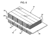
Fig. 6 is a perspective view of a detector
module using a semiconductor detector according to a
second embodiment of the present invention;
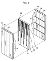
Fig. 7 is an exploded perspective view
showing the semiconductor radiation detector in Fig. 6;
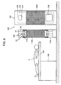
Fig. 8 is a longitudinal cross-sectional view
of a PET-X-ray CT examination apparatus provided with a
PET examination apparatus using the detector module in
Fig. 4 according to a third embodiment of the present
invention;
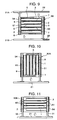
Fig. 9 is a cross-sectional view showing a
semiconductor radiation detector according to a first
modification example of the present invention;
Fig. 10 is a cross-sectional view showing a
semiconductor radiation detector according to a second
modification example of the present invention;
Fig. 11 is a cross-sectional view showing a
semiconductor radiation detector according to a third
modification example of the present invention;
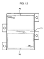
Fig. 12 is a plan view showing a
semiconductor radiation detector according to a fourth
modification example of the present invention;
Fig. 13 is a plan view showing a
semiconductor radiation detector according to a fifth
modification example of the present invention;
Fig. 14 is an assembly diagram showing the
semiconductor radiation detector according to the fifth
modification example of the present invention;
Fig. 15 is a plan view showing a
semiconductor radiation detector according to a sixth
modification example of the present invention;
Fig. 16 is a plan view showing a
semiconductor radiation detector according to a seventh
modification example of the present invention; and
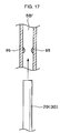
Fig. 17 is an exploded diagram showing a pin
insertion hole and elastic bodies, etc., according to
an eighth modification example of the present
invention.
DESCRIPTION OF THE EMBODIMENTS
With reference now to the attached drawings
of Figs. 1 to 5, a first embodiment of the present
invention will be explained below.
(First embodiment)
Reference numeral 1 in Fig. 1 denotes a
radiation detection device and this radiation detection
device 1 is constructed by including five semiconductor
devices 2 (see Fig. 2) made up of a rectangular flat
plate made of, for example, CdTe, cathode electrodes 3
(Pt, etc.) formed into a thin-film shape on one side of
each semiconductor device 2 by means of, for example,
vapor deposition, anode electrodes 4 (In, etc.) formed
into a thin-film shape on the other side of the
semiconductor device 2 and a rectangular parallelepiped
elastic insulator 5 (see Fig. 2) which covers the five
semiconductor devices 2 from the outside.
As shown in Fig. 2, this semiconductor
radiation device 1 consists of five semiconductor
devices 2 stacked together. Furthermore, conductive
cathode-side thin plates 6 are pasted to the respective
cathode electrodes 3 and conductive anode-side thin
plates 7 are pasted to the respective anode electrodes
4. First and second internal wirings 8, 9 provide
connections among the thin plates 6 and the thin plates
7, respectively. Furthermore, rectangular
parallelepiped brackets 5A, 5A are formed integral with
the insulator 5 on both sides in its width direction
and pin insertion holes 5B are formed in these brackets
5A in the longitudinal direction thereof so that a
cathode pin 29 and an anode pin 30 which will be
described later are inserted therein. Furthermore, a
cathode terminal 10 to be connected to the first
internal wiring 8 is exposed from an end face of the
one bracket 5A to the outside and an anode terminal 11
to be connected to the second internal wiring 9 is
exposed from an end face of the other bracket 5A to the
outside. The semiconductor devices 2, cathode
electrodes 3, anode electrodes 4, insulator 5, thin
plates 6, 7, internal wirings 8, 9, cathode terminal 10
and anode terminal 11 constitute a semiconductor
radiation detector 12. Note that the structures of the
first internal wiring 8 and cathode terminal 10, and
the second internal wiring 9 and anode terminal 11 can
be simplified by forming inner walls of the respective
pin insertion holes 5B using a conductive material and
connecting the thin plates 6 and 7 with the conductive
inner walls.
In Fig. 4, reference numeral 21 denotes a
wiring board used for this embodiment and first cathode
wirings 22 arranged in parallel to one another, a
second cathode wiring 23 which extends perpendicular to
the respective cathode wirings 22 and connects the
cathode wirings 22 and a third cathode wiring 24 which
extends rightward from the cathode wiring 22 at the top
end in Fig. 4 are buried in this wiring board 21.
These cathode wirings 22, 23 and 24 are electrically
connected and the same potential is supplied from the
outside of the wiring board 21 to the cathode
electrodes 3 of all the detectors. The plurality of
semiconductor radiation detectors 12 and the wiring
board 21 in which these semiconductor radiation
detectors 12 are arranged constitute a detector module
42. The detector module 42 also includes a plurality
of cathode wiring and a plurality of anode wirings.
Furthermore, first anode wirings 25 arranged
parallel to one another, second anode wirings 26
arranged parallel to one another, third anode wirings
27 arranged parallel to one another and fourth anode
wirings 28 arranged parallel to one another are buried
in the wiring board 21.
Then, as shown in Fig. 4 and Fig. 5, cathode
pins 29 are formed in an upright position on the
cathode wiring 22, spaced substantially uniformly on
one side and the other side of the wiring board 21.
Furthermore, anode pins 30 are also formed in an
upright position at the ends of the first, second,
third anode wirings 25, 26, 27 spaced substantially
uniformly on one side and the other side of the wiring
board 21.
Then, the semiconductor radiation detector 12
is inserted in a detachable manner in the direction
indicated by an arrow A in Fig. 5 with a cathode pin 29
and an anode pin 30 fitted in the pin insertion holes
5B, 5B of the elastic insulator 5 with clamping
margins. The semiconductor radiation detector 12 may
also be directly fixed to the wiring board 21 using a
conductive space, etc., instead of the cathode pin 29
and anode pin 30. In this case, instead of the pin
insertion holes 5B, the insulator 5 is provided with
plated wiring and the ends of this plated wiring are
used as a cathode terminal 10 and an anode terminal 11.
A conductive paste, etc., may be applied to these
cathode terminal 10 and anode terminal 11, which may be
then fixed to the wiring board 21.
Then, the operation of the semiconductor
radiation detector 12 having such a structure will be
explained.
A negative voltage is applied to the cathode
electrodes 3 of the semiconductor device 2 from the
outside of the wiring board 21 through the cathode
wirings 22, 23, 24, a reverse bias voltage is formed
between the cathode electrodes 3 and anode electrodes 4
of the semiconductor device 2 so that γ-rays can be
measured. When γ-rays enter the semiconductor device 2,
electric charge is induced between the cathode
electrodes 3 and anode electrodes 4 set in the
semiconductor device 2, and signals corresponding to
the amount of charge induced are output from the anode
wirings 25, 26, 27, 28 to the outside through a thin
plate 7, internal wiring 9, anode terminal 11 and anode
pin 30.
This embodiment allows γ-rays to be detected
by separating their positions in the direction of
incidence of γ-rays, too, and further allows γ-rays to
be detected with their positions separated in the
three-dimensional direction. Furthermore, covering
with an insulator facilitates handling of the
semiconductor radiation detector in manufacturing,
etc., and can physically protect the radiation
detection devices.
Furthermore, according to the method of using
the cathode pin 29 and anode pin 30, the semiconductor
radiation detector 12 is mounted on the wiring board 21
in a detachable manner, and it is possible to thereby
replace any semiconductor radiation detector 12 and
improve operability, etc., in the case of replacement.
Furthermore, the entire semiconductor device
2 is covered with the insulator 5, and therefore it is
possible to produce the moisture-proof effect and
light-shielding effect on the semiconductor radiation
detector 12.
(Second embodiment)
Then, a second embodiment of the present
invention will be explained with reference to the
attached drawings of Fig. 6 and Fig. 7. In Fig. 6, a
plurality of semiconductor radiation detectors 31 are
constructed by including thin wiring boards 32 with
flexibility called "FPC (Flexible printed circuit)",
semiconductor devices 33 mounted on both sides of the
thin wiring boards 32, cathode electrodes 34 formed in
a thin-film shape on one side of the semiconductor
devices 33 through vapor deposition, etc., and anode
electrodes 35 formed on the other side of the
semiconductor devices 33.
The semiconductor devices 33 are arranged in
four rows in the direction in which γ-rays propagate
with a small gap interposed between neighboring devices
and also arranged in four rows in the direction
orthogonal to the direction in which γ-rays propagate
with a small gap interposed between neighboring
devices. Furthermore, the semiconductor radiation
detectors 31 are mounted fixed to both sides of a thick
wiring board (FR-4, etc.) 36. A plurality of
semiconductor radiation detectors 31 mounted on both
sides of the thick wiring board 36 constitute a
detector module 43. Note that it is also possible to
construct the semiconductor devices 33 using one
crystal on the same plane and by dividing only the
electrodes.
Furthermore, in the thin wiring boards 32
interposed between the facing anode electrodes 35, 35,
four signal lines 38, 39, 40 and 41, which extend to
the positions corresponding to the anode electrodes 35
of the respective semiconductor devices 33 to be
connected to the respective anode electrodes 35 are
buried as shown in Fig. 7.
On the other hand, in the thin wiring boards
32 interposed between the facing cathode electrodes 34,
34, supply lines (not shown) for applying a voltage
common to all cathodes are buried in the cathode
electrodes 34 and these signal lines are connected to
the cathode electrodes 34 of the plurality of
semiconductor devices 33 arranged along the direction
of incidence of γ-rays.
The above described supply lines connected to
the cathode electrodes 34 are connected to cathode
wiring (not shown) of the thick wiring board 36 and the
signal lines 38, 39, 40 and 41 are connected to the
respective anode wirings (not shown) of the thick
wiring board 36.
Note that the thick wiring boards 36 may be
replaced by the thin wiring boards 32.
This embodiment having such a structure can
also detect γ-rays by separating positions in the three-dimensional
direction as with the first embodiment.
Furthermore, it is also possible to reduce spacing
between the plurality of semiconductor devices 31 and
improve sensitivity.
(Third embodiment)
Then, a third embodiment of the present
invention will be explained with reference to the
attached drawing of Fig. 8. The same components in
this embodiment as those in the first embodiment are
assigned the same reference numerals and explanations
thereof will be omitted.
As shown in Fig. 8, a PET-X-ray CT
examination apparatus 100, which is a radiation imaging
apparatus, comprises an X-ray CT examination apparatus
101 and a PET examination apparatus 102 side by side.
Furthermore, the PET-X-ray CT examination apparatus 100
includes a bed holding section 103 and a movable bed
104 provided on the bed holding section 103. Then, the
X-ray CT examination apparatus 101 is provided with an
X-ray CT gantry 105 having an opening 105A, a rotary
section 106 rotatably mounted in the X-ray CT gantry
105, an X-ray generator 107 provided in the rotary
section 106 and a radiation detector 108, which is a
scintillator detector provided in the rotary section
106. Then, this X-ray CT examination apparatus 101
measures X-rays which are emitted from the X-rays
generator 107 and have passed through an examinee P
using a signal processing section (not shown) and
obtains a mode image of the interior of the examinee P.
Furthermore, the PET examination apparatus
102 includes a PET gantry 110 having an opening 110A
and the PET gantry 110 has a plurality of detector
modules 42 arranged in the circumferential direction
and axial direction. For this reason, a plurality of
radiation detectors 12 are also arranged in the
circumferential direction and axial direction of the
PET gantry 110. The PET examination apparatus 102 is a
radiation imaging apparatus which marks radionuclides
which emit positrons through nucleorrhexis in
chemicals, administers the chemicals into the examinee
P, captures pairs of γ-rays having 511 keV energy which
are emitted when pairs of positron and electron are
annihilated in the body of the examinee P and creates
images of them as functional images.
This embodiment having such a structure can
mount the semiconductor radiation detectors 12 densely
on both sides of the wiring board 21 as described in
the conventional art, thereby increase the density of
the semiconductor radiation detectors 12 per a unit
length of the wiring board 21 in the detector module
42, improve the detection sensitivity and improve the
performance and reliability of the PET-X-ray CT
examination apparatus 100.
The PET examination apparatus 102 may also
mount the detector module 43 shown in Fig. 6 in the PET
gantry 110 instead of the detector module 42 as with
the detector module 42.
As shown in Fig. 5, the first embodiment has
described the case where the terminals of both the
cathode terminal 10 and anode terminal 11 are exposed
from one side of the insulator 5 which is a rectangular
parallelepiped and the semiconductor radiation
detectors 12 are fixed to both sides of the wiring
board 21 using the cathode pin 29 and anode pin 30 as
an example.
However, the present invention is not limited
to this but can be adapted so that as shown in a first
modification example shown in Fig. 9, a cathode pin 51
is inserted from one side of an insulator 54 of a
semiconductor radiation detector 50 and an anode pin 55
is inserted from the other side of the insulator 54 of
the semiconductor radiation detector 50. In this case,
the cathode pin 51 is connected to a cathode wiring 22
buried in a wiring board 21A and the anode pin 55 is
connected to an anode wiring 25 buried in a wiring
board 21B.
Furthermore, for example, as a second
modification example shown in Fig. 10, it is also
possible to adopt a structure in which a semiconductor
radiation detector 50A is placed in a direction
perpendicular to a wiring board 21, and a cathode pin
51 and an anode pin 55 disposed on the wiring board 21
in an upright position are inserted into the
semiconductor radiation detector 50A.
Furthermore, in a semiconductor radiation
detector 50B which is a third modification example
shown in Fig. 11, a plurality of radiation detection
devices 1 are arranged in a staggered configuration and
internal wirings 62 are connected to anode electrodes
of the radiation detection devices 1 protruding in one
direction out of these radiation detection devices 1.
Furthermore, internal wirings 61 are connected to
cathode electrodes of the radiation detection devices 1
protruding in the other direction out of these
radiation detection devices 1. The cathode pin 51 and
anode pin 55 are connected to these internal wirings
61, 62.
The first embodiment has described the case
where a plurality of semiconductor radiation detectors
12 are mounted on the wiring board 21 independently of
one another through gaps as an example, but the present
invention is not limited to this and can be adapted as
a fourth modification example shown in Fig. 12 so that
insulators 71 of neighboring semiconductor radiation
detectors 70 are united.
The first embodiment has also described the
case where the entire semiconductor radiation detector
1 is coated with the insulator 5 as an example, but the
present invention is not limited to this and can be
adapted so that as in the case of a fifth modification
example shown in Fig. 13 and Fig. 14, for example, a
semiconductor radiation detector 80 is provided with
insulators 81, 82 partially having pin insertion holes
81A, 82A and cathode socket (e.g., hollow metal pipe)
83 and anode socket 84 are provided inside the pin
insertion holes 81A, 82A of this insulator 81 so that
the cathode pin 85 is inserted into the cathode socket
83 and the anode pin 86 is inserted into the anode
socket 84.
In this case, it is also possible to adopt a
structure as a sixth modification example shown in Fig.
15, for example, in which two neighboring semiconductor
radiation detectors 90, 90 are partially provided with
insulators 91, 92 and the two semiconductor radiation
detectors 90, 90 are kept insulated from each other by
means of a common insulating plate 93.
Furthermore, it is also possible to adopt a
structure as a seventh modification example shown in
Fig. 16, for example, in which a pin insertion hole 94A
on the cathode side is provided at one end of a common
insulator 94 attached to two neighboring semiconductor
radiation detectors 90 and pin insertion holes 94B, 94B
on the anode side are provided at the other end of the
insulator 94.
Moreover, the first embodiment has described
the case where the cathode pin 29 and anode pin 30
having a slightly greater diameter than the diameter of
the pin insertion holes 5B are fitted into these pin
insertion holes 5B utilizing elasticity thereof as an
example, but the present invention is not limited to
this and, for example, as in the case of an eighth
modification example shown in Fig. 17, hemispherical
elastic bodies 95, 95 are attached to the inner
surfaces of a pin insertion hole 5B' and a cathode pin
29 or anode pin 30 is inserted into a pin insertion
hole 5B' in such a way as to be pushed by the elastic
bodies 95, 95 from both sides.
In the above described modification examples,
if detachability is not essential, it is possible to
directly fix semiconductor radiation detectors to the
wiring board using not the aforementioned cathode pin
and anode pin but a conductive paste, etc. In this
case, instead of pin insertion holes, plated wiring is
applied to the insulator 5 and the ends of this plated
wiring are used as a cathode terminal 10 and anode
terminal 11. A conductive paste, etc., may be applied
to this cathode terminal 10 and anode terminal 11 and
fixed to the wiring board 21.
Furthermore, in the first embodiment, the
output ends of the anode and cathode of the
semiconductor radiation detector are arranged at
diagonal positions of the semiconductor device, but
their positions are not limited to this and their
output ends may be arranged on the same side of the
semiconductor detection device and a wiring pattern
corresponding to the output end positions may be used
for the wiring board in this case.
It should be further understood by those
skilled in the art that although the foregoing
description has been made on embodiments of the
invention, the invention is not limited thereto and
various changes and modifications may be made without
departing from the spirit of the invention and the
scope of the appended claims.