EP1521093A1 - Design analysis technique - Google Patents
Design analysis technique Download PDFInfo
- Publication number
- EP1521093A1 EP1521093A1 EP03021995A EP03021995A EP1521093A1 EP 1521093 A1 EP1521093 A1 EP 1521093A1 EP 03021995 A EP03021995 A EP 03021995A EP 03021995 A EP03021995 A EP 03021995A EP 1521093 A1 EP1521093 A1 EP 1521093A1
- Authority
- EP
- European Patent Office
- Prior art keywords
- test
- lrt
- analysis technique
- design
- pattern
- Prior art date
- Legal status (The legal status is an assumption and is not a legal conclusion. Google has not performed a legal analysis and makes no representation as to the accuracy of the status listed.)
- Granted
Links
Images
Classifications
-
- G—PHYSICS
- G01—MEASURING; TESTING
- G01R—MEASURING ELECTRIC VARIABLES; MEASURING MAGNETIC VARIABLES
- G01R31/00—Arrangements for testing electric properties; Arrangements for locating electric faults; Arrangements for electrical testing characterised by what is being tested not provided for elsewhere
- G01R31/28—Testing of electronic circuits, e.g. by signal tracer
- G01R31/317—Testing of digital circuits
- G01R31/3181—Functional testing
- G01R31/3183—Generation of test inputs, e.g. test vectors, patterns or sequences
- G01R31/318342—Generation of test inputs, e.g. test vectors, patterns or sequences by preliminary fault modelling, e.g. analysis, simulation
- G01R31/318357—Simulation
-
- G—PHYSICS
- G01—MEASURING; TESTING
- G01R—MEASURING ELECTRIC VARIABLES; MEASURING MAGNETIC VARIABLES
- G01R31/00—Arrangements for testing electric properties; Arrangements for locating electric faults; Arrangements for electrical testing characterised by what is being tested not provided for elsewhere
- G01R31/28—Testing of electronic circuits, e.g. by signal tracer
- G01R31/317—Testing of digital circuits
- G01R31/3181—Functional testing
- G01R31/3183—Generation of test inputs, e.g. test vectors, patterns or sequences
- G01R31/318371—Methodologies therefor, e.g. algorithms, procedures
-
- G—PHYSICS
- G06—COMPUTING OR CALCULATING; COUNTING
- G06F—ELECTRIC DIGITAL DATA PROCESSING
- G06F30/00—Computer-aided design [CAD]
- G06F30/20—Design optimisation, verification or simulation
Definitions
- the invention concerns a design analysis technique for a test pattern analysis of chips via an automatic test equipment (ATE) or a circuit simulation to detect potential design weakness or abnormal behavior in real customer application faults.
- ATE automatic test equipment
- Typical test pattern analysis via ATE or circuit simulation is very difficult to detect potential design weakness or abnormal behavior in real customer application faults. There are a lot of cases that customers have a problem to run the chip while even through the chip passed all tests in the producers analysis lab.
- the major technical problem and challenge is how to perform a test or develop a technique which can cover or at least close to the test in real customer application via ATE or a complete circuit simulation based on the real customer application, but without using the real customer application setup e.g. the hardware and the software.
- Another object of the invention is to provide an analysis technique which actually shows when the chip fails and how it fails.
- Another object of the invention is to provide an analysis technique for a much longer test sequence.
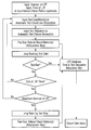
- the problems are solved by comprising a simulation procedure stored in a LRT database of a automatic test equipment (ATE), defining test conditions and test patterns which executes and generates continuously for a time given by a user, applying the test stimuli and test conditions to a device under test (DUT) and starting the long running test (LRT), stop the test automatically if any application faults occurs and log the failure time and timely test sequence and starting another test again until a given maximum number of test is reached.
- ATE automatic test equipment
- the long running test is started with pre-defined long running test conditions which are run time and run time per test.
- the design defective or weakness due to application failures is identified by a small set of test pattern, test condition, LRT failure time and robustness check.
- the invention solves all technical problems mentioned in the prior art description by a long running test (LRT) concept.
- LRT long running test
- the main concept of the LRT imitate the application test behavior and condition. All dedicated test conditions and test pattern are executing or generating continuously for a time given by a user.
- the running time can be a few hours, days or a few minutes, seconds etc.
- the testing time is similar to the application test so that if any application fault occurs, the test will automatically stop and log the failure time and timely test sequence.
- Such a scheme can efficiently identify a defective and weakness due to application failure as well as locate the defect or weakness within design in a much shorter time compares to typical way according the prior art. This is the major advantage of the invention, while conventional way of testing can not handle such a problem systematically and efficiently.
- test run time the LRT loops
- test condition generation the test condition generation
- test pattern generation the test pattern generation
- ATE automatic test equipment
- test stimuli and test conditions are applied to a device under test (DUT).
- DUT device under test
- LRT long running test
- end of LRT can optional applied a post-check of robust check pattern to the device under test (DUT) and record the output of test results (pass or fail) under the same test conditions into final database.
- DUT device under test
- test pattern (worst case timely test sequence with respect to LRT failure), test condition, LRT failure time and robustness check, are used to identify the design defective or weakness due to application failures.
- circuit simulation analysis based on the foregoing information to localize the design defective and weakness including wafer probing internal signal with respect to worst case test pattern and condition.
- test conditions are defined with customer requirement to screen out the first design engineering sample (ES).
- test conditions are a three core of power supply.
- E.g. 1, 7 V (low), 1,8 V (norm) and 1,95 V (high), TRC (device row cycle time) is 70 nsec
- test pattern with refresh logic turn on and off and each LRT with dedicated power supply level run continuously for 3 hours.
- the tested chip hang on less than 30 sec at low power supply level of 1,7 V with refresh on, it is provided by post test robust pattern failed at all data output bus are actually stuck at some values while other command signals hang up at some states.
- the chip does not hang up at low power supply level of 1, 7 V with refresh off.
Landscapes
- Engineering & Computer Science (AREA)
- General Engineering & Computer Science (AREA)
- Physics & Mathematics (AREA)
- General Physics & Mathematics (AREA)
- Computer Hardware Design (AREA)
- Theoretical Computer Science (AREA)
- Evolutionary Computation (AREA)
- Geometry (AREA)
- Tests Of Electronic Circuits (AREA)
Abstract
Description
Claims (7)
- Design analysis technique for a test pattern analysis of chips via an automatic test equipment (ATE) or a circuit simulation to detect potential design weakness or abnormal behavior in real customer application faults comprising a simulation procedure stored in a LRT database of a automatic test equipment (ATE), defining test conditions and test patterns which executes and generates continuously for a time given by a user, applying the test stimuli and test conditions to a device under test (DUT) and starting the long running test (LRT), stop the test automatically if any application faults occurs and log the failure time and timely test sequence and starting another test again until a given maximum number of test is reached.
- Design analysis technique according claim 1 comprising applying a pre-check of robust check pattern to the device under test and recording the output of the test results (pass or fail) under the same test condition into LRT database.
- Design analysis technique according claim 1 comprising starting the long running test with pre-defined long running test conditions.
- Design analysis technique according claim 3 characterized in that the pre defined long running test conditions are run time and run time per test.
- Design analysis technique according one of the claims 1 to 4 comprising applying a post-check of robust check pattern to the device under test and record the output of the test results (pass or fail) under the same test conditions into final database.
- Design analysis technique according one of the claims 1 to 5 comprising identifying the design defective or weakness due to application failures by a small set of test pattern, test condition, LRT failure time and robustness check.
- Design analysis technique according claim 6 comprising localizing the design defective and weakness based on LRT failure time and test sequence by circuit simulation.
Priority Applications (3)
| Application Number | Priority Date | Filing Date | Title |
|---|---|---|---|
| DE60303168T DE60303168T2 (en) | 2003-09-30 | 2003-09-30 | Method for the long-term analysis of a circuit design |
| EP03021995A EP1521093B1 (en) | 2003-09-30 | 2003-09-30 | Long running test method for a circuit design analysis |
| US10/954,983 US7210086B2 (en) | 2003-09-30 | 2004-09-30 | Long running test method for a circuit design analysis |
Applications Claiming Priority (1)
| Application Number | Priority Date | Filing Date | Title |
|---|---|---|---|
| EP03021995A EP1521093B1 (en) | 2003-09-30 | 2003-09-30 | Long running test method for a circuit design analysis |
Publications (2)
| Publication Number | Publication Date |
|---|---|
| EP1521093A1 true EP1521093A1 (en) | 2005-04-06 |
| EP1521093B1 EP1521093B1 (en) | 2006-01-11 |
Family
ID=34306789
Family Applications (1)
| Application Number | Title | Priority Date | Filing Date |
|---|---|---|---|
| EP03021995A Expired - Lifetime EP1521093B1 (en) | 2003-09-30 | 2003-09-30 | Long running test method for a circuit design analysis |
Country Status (3)
| Country | Link |
|---|---|
| US (1) | US7210086B2 (en) |
| EP (1) | EP1521093B1 (en) |
| DE (1) | DE60303168T2 (en) |
Cited By (1)
| Publication number | Priority date | Publication date | Assignee | Title |
|---|---|---|---|---|
| US9552449B1 (en) | 2016-01-13 | 2017-01-24 | International Business Machines Corporation | Dynamic fault model generation for diagnostics simulation and pattern generation |
Families Citing this family (10)
| Publication number | Priority date | Publication date | Assignee | Title |
|---|---|---|---|---|
| CN101022719B (en) | 2004-09-16 | 2010-06-09 | 克罗普迪塞恩股份有限公司 | Method and apparatus for evaluating plant roots |
| US20060195744A1 (en) * | 2005-02-11 | 2006-08-31 | Broadcom Corporation | Method and apparatus to simulate automatic test equipment |
| KR100809598B1 (en) * | 2006-06-20 | 2008-03-04 | 삼성전자주식회사 | Semiconductor test system capable of virtual test and its semiconductor test method |
| CN102159065A (en) | 2008-09-16 | 2011-08-17 | 巴斯夫植物科学有限公司 | Improved plant breeding method |
| US8350586B2 (en) * | 2009-07-02 | 2013-01-08 | Taiwan Semiconductor Manufacturing Company, Ltd. | Method and apparatus of deembedding |
| US8661293B2 (en) | 2011-06-30 | 2014-02-25 | International Business Machines Corporation | Test architecture based on intelligent test sequence |
| US20150052616A1 (en) * | 2013-08-14 | 2015-02-19 | L-3 Communications Corporation | Protected mode for securing computing devices |
| IN2013DE02948A (en) * | 2013-10-04 | 2015-04-10 | Unisys Corp | |
| CN111105839B (en) * | 2018-10-26 | 2022-04-15 | 长鑫存储技术有限公司 | Chip testing method and device, electronic equipment and computer readable medium |
| CN116935943A (en) * | 2022-03-30 | 2023-10-24 | 富联精密电子(天津)有限公司 | Automatic test method, equipment and storage medium |
Citations (3)
| Publication number | Priority date | Publication date | Assignee | Title |
|---|---|---|---|---|
| US6098186A (en) * | 1998-05-29 | 2000-08-01 | Hewlett-Packard Company | Test permutator |
| US6115835A (en) * | 1997-06-10 | 2000-09-05 | Micron Technology, Inc. | Method and apparatus for determining a set of tests for integrated circuit testing |
| US6347386B1 (en) * | 1996-08-07 | 2002-02-12 | Micron Technology, Inc. | System for optimizing the testing and repair time of a defective integrated circuit |
Family Cites Families (3)
| Publication number | Priority date | Publication date | Assignee | Title |
|---|---|---|---|---|
| US6070260A (en) * | 1998-09-17 | 2000-05-30 | Xilinx, Inc. | Test methodology based on multiple skewed scan clocks |
| US6651202B1 (en) * | 1999-01-26 | 2003-11-18 | Lsi Logic Corporation | Built-in self repair circuitry utilizing permanent record of defects |
| US20050024074A1 (en) * | 2003-08-01 | 2005-02-03 | Gary Benjamin | Method and apparatus for characterizing an electronic circuit |
-
2003
- 2003-09-30 EP EP03021995A patent/EP1521093B1/en not_active Expired - Lifetime
- 2003-09-30 DE DE60303168T patent/DE60303168T2/en not_active Expired - Lifetime
-
2004
- 2004-09-30 US US10/954,983 patent/US7210086B2/en not_active Expired - Fee Related
Patent Citations (3)
| Publication number | Priority date | Publication date | Assignee | Title |
|---|---|---|---|---|
| US6347386B1 (en) * | 1996-08-07 | 2002-02-12 | Micron Technology, Inc. | System for optimizing the testing and repair time of a defective integrated circuit |
| US6115835A (en) * | 1997-06-10 | 2000-09-05 | Micron Technology, Inc. | Method and apparatus for determining a set of tests for integrated circuit testing |
| US6098186A (en) * | 1998-05-29 | 2000-08-01 | Hewlett-Packard Company | Test permutator |
Cited By (1)
| Publication number | Priority date | Publication date | Assignee | Title |
|---|---|---|---|---|
| US9552449B1 (en) | 2016-01-13 | 2017-01-24 | International Business Machines Corporation | Dynamic fault model generation for diagnostics simulation and pattern generation |
Also Published As
| Publication number | Publication date |
|---|---|
| EP1521093B1 (en) | 2006-01-11 |
| US7210086B2 (en) | 2007-04-24 |
| DE60303168T2 (en) | 2006-08-17 |
| DE60303168D1 (en) | 2006-04-06 |
| US20050108608A1 (en) | 2005-05-19 |
Similar Documents
| Publication | Publication Date | Title |
|---|---|---|
| US6971054B2 (en) | Method and system for determining repeatable yield detractors of integrated circuits | |
| CN109840207B (en) | AutoSAR-based network management automation test system and test method | |
| US7934134B2 (en) | Method and apparatus for performing logic built-in self-testing of an integrated circuit | |
| EP1521093A1 (en) | Design analysis technique | |
| Huang et al. | Compressed pattern diagnosis for scan chain failures | |
| US7480882B1 (en) | Measuring and predicting VLSI chip reliability and failure | |
| CN114631031A (en) | Automated test equipment, process and computer program for testing one or more devices under test, wherein different test activities utilize a subset of device under test resources | |
| US6557132B2 (en) | Method and system for determining common failure modes for integrated circuits | |
| US20030053358A1 (en) | Dft technique for avoiding contention/conflict in logic built-in self-test | |
| US11092645B2 (en) | Chain testing and diagnosis using two-dimensional scan architecture | |
| US7571367B2 (en) | Built-in self diagnosis device for a random access memory and method of diagnosing a random access | |
| JP2680259B2 (en) | Automatic opening detection method | |
| CN119068958B (en) | DRAM test machine and method based on embedded logic analysis | |
| US6480011B2 (en) | Screening of semiconductor integrated circuit devices | |
| US5293387A (en) | Method for increasing the resolution of a digital fault dictionary | |
| Filipponi et al. | In-field data collection system through logic bist for large automotive systems-on-chip | |
| JP2006105997A (en) | Method and apparatus for providing a scan pattern to an electronic device | |
| US20020099993A1 (en) | Semiconductor testing apparatus and method | |
| JPH09185519A (en) | Debugging device for ic test program | |
| Kabir et al. | Performance analysis of a new low power BIST technique in VLSI circuit by reducing the input vectors | |
| US20110035638A1 (en) | Timing Failure Debug | |
| US20090210761A1 (en) | AC Scan Diagnostic Method and Apparatus Utilizing Functional Architecture Verification Patterns | |
| Shisha et al. | Enhanced Diagnosis of Failing Bits in Memory Built-in Self-Test | |
| CN107167675A (en) | A kind of ageing testing method and device of CANBus terminals | |
| US7461315B2 (en) | Method and system for improving quality of a circuit through non-functional test pattern identification |
Legal Events
| Date | Code | Title | Description |
|---|---|---|---|
| PUAI | Public reference made under article 153(3) epc to a published international application that has entered the european phase |
Free format text: ORIGINAL CODE: 0009012 |
|
| 17P | Request for examination filed |
Effective date: 20040617 |
|
| AK | Designated contracting states |
Kind code of ref document: A1 Designated state(s): AT BE BG CH CY CZ DE DK EE ES FI FR GB GR HU IE IT LI LU MC NL PT RO SE SI SK TR |
|
| AX | Request for extension of the european patent |
Extension state: AL LT LV MK |
|
| GRAP | Despatch of communication of intention to grant a patent |
Free format text: ORIGINAL CODE: EPIDOSNIGR1 |
|
| RTI1 | Title (correction) |
Free format text: LONG RUNNING TEST METHOD FOR A CIRCUIT DESIGN ANALYSIS |
|
| RIC1 | Information provided on ipc code assigned before grant |
Ipc: 7G 01R 31/317 B Ipc: 7G 01R 31/3183 A Ipc: 7G 06F 17/50 B |
|
| RTI1 | Title (correction) |
Free format text: LONG RUNNING TEST METHOD FOR A CIRCUIT DESIGN ANALYSIS |
|
| GRAS | Grant fee paid |
Free format text: ORIGINAL CODE: EPIDOSNIGR3 |
|
| GRAA | (expected) grant |
Free format text: ORIGINAL CODE: 0009210 |
|
| AKX | Designation fees paid |
Designated state(s): DE GB IE |
|
| AK | Designated contracting states |
Kind code of ref document: B1 Designated state(s): DE GB IE |
|
| REG | Reference to a national code |
Ref country code: IE Ref legal event code: FG4D |
|
| REF | Corresponds to: |
Ref document number: 60303168 Country of ref document: DE Date of ref document: 20060406 Kind code of ref document: P |
|
| PLBE | No opposition filed within time limit |
Free format text: ORIGINAL CODE: 0009261 |
|
| STAA | Information on the status of an ep patent application or granted ep patent |
Free format text: STATUS: NO OPPOSITION FILED WITHIN TIME LIMIT |
|
| 26N | No opposition filed |
Effective date: 20061012 |
|
| GBPC | Gb: european patent ceased through non-payment of renewal fee |
Effective date: 20070930 |
|
| PG25 | Lapsed in a contracting state [announced via postgrant information from national office to epo] |
Ref country code: GB Free format text: LAPSE BECAUSE OF NON-PAYMENT OF DUE FEES Effective date: 20070930 |
|
| REG | Reference to a national code |
Ref country code: DE Ref legal event code: R081 Ref document number: 60303168 Country of ref document: DE Owner name: INFINEON TECHNOLOGIES AG, DE Free format text: FORMER OWNER: QIMONDA AG, 81739 MUENCHEN, DE Ref country code: DE Ref legal event code: R081 Ref document number: 60303168 Country of ref document: DE Owner name: POLARIS INNOVATIONS LTD., IE Free format text: FORMER OWNER: QIMONDA AG, 81739 MUENCHEN, DE |
|
| REG | Reference to a national code |
Ref country code: DE Ref legal event code: R081 Ref document number: 60303168 Country of ref document: DE Owner name: POLARIS INNOVATIONS LTD., IE Free format text: FORMER OWNER: INFINEON TECHNOLOGIES AG, 85579 NEUBIBERG, DE |
|
| PGFP | Annual fee paid to national office [announced via postgrant information from national office to epo] |
Ref country code: IE Payment date: 20160909 Year of fee payment: 14 |
|
| PGFP | Annual fee paid to national office [announced via postgrant information from national office to epo] |
Ref country code: DE Payment date: 20160927 Year of fee payment: 14 |
|
| REG | Reference to a national code |
Ref country code: DE Ref legal event code: R119 Ref document number: 60303168 Country of ref document: DE |
|
| REG | Reference to a national code |
Ref country code: IE Ref legal event code: MM4A |
|
| PG25 | Lapsed in a contracting state [announced via postgrant information from national office to epo] |
Ref country code: DE Free format text: LAPSE BECAUSE OF NON-PAYMENT OF DUE FEES Effective date: 20180404 Ref country code: IE Free format text: LAPSE BECAUSE OF NON-PAYMENT OF DUE FEES Effective date: 20170930 |