EP1519308A2 - Power conditioning mechanism using an external card adapter - Google Patents
Power conditioning mechanism using an external card adapter Download PDFInfo
- Publication number
- EP1519308A2 EP1519308A2 EP04018122A EP04018122A EP1519308A2 EP 1519308 A2 EP1519308 A2 EP 1519308A2 EP 04018122 A EP04018122 A EP 04018122A EP 04018122 A EP04018122 A EP 04018122A EP 1519308 A2 EP1519308 A2 EP 1519308A2
- Authority
- EP
- European Patent Office
- Prior art keywords
- power
- external card
- adaptor
- computing device
- card
- Prior art date
- Legal status (The legal status is an assumption and is not a legal conclusion. Google has not performed a legal analysis and makes no representation as to the accuracy of the status listed.)
- Withdrawn
Links
Images

Classifications
-
- G—PHYSICS
- G06—COMPUTING OR CALCULATING; COUNTING
- G06K—GRAPHICAL DATA READING; PRESENTATION OF DATA; RECORD CARRIERS; HANDLING RECORD CARRIERS
- G06K19/00—Record carriers for use with machines and with at least a part designed to carry digital markings
- G06K19/06—Record carriers for use with machines and with at least a part designed to carry digital markings characterised by the kind of the digital marking, e.g. shape, nature, code
- G06K19/067—Record carriers with conductive marks, printed circuits or semiconductor circuit elements, e.g. credit or identity cards also with resonating or responding marks without active components
- G06K19/07—Record carriers with conductive marks, printed circuits or semiconductor circuit elements, e.g. credit or identity cards also with resonating or responding marks without active components with integrated circuit chips
- G06K19/077—Constructional details, e.g. mounting of circuits in the carrier
- G06K19/07737—Constructional details, e.g. mounting of circuits in the carrier the record carrier consisting of two or more mechanically separable parts
- G06K19/07741—Constructional details, e.g. mounting of circuits in the carrier the record carrier consisting of two or more mechanically separable parts comprising a first part operating as a regular record carrier and a second attachable part that changes the functional appearance of said record carrier, e.g. a contact-based smart card with an adapter part which, when attached to the contact card makes the contact card function as a non-contact card
-
- G—PHYSICS
- G06—COMPUTING OR CALCULATING; COUNTING
- G06K—GRAPHICAL DATA READING; PRESENTATION OF DATA; RECORD CARRIERS; HANDLING RECORD CARRIERS
- G06K19/00—Record carriers for use with machines and with at least a part designed to carry digital markings
- G06K19/06—Record carriers for use with machines and with at least a part designed to carry digital markings characterised by the kind of the digital marking, e.g. shape, nature, code
- G06K19/067—Record carriers with conductive marks, printed circuits or semiconductor circuit elements, e.g. credit or identity cards also with resonating or responding marks without active components
- G06K19/07—Record carriers with conductive marks, printed circuits or semiconductor circuit elements, e.g. credit or identity cards also with resonating or responding marks without active components with integrated circuit chips
- G06K19/077—Constructional details, e.g. mounting of circuits in the carrier
-
- G—PHYSICS
- G06—COMPUTING OR CALCULATING; COUNTING
- G06K—GRAPHICAL DATA READING; PRESENTATION OF DATA; RECORD CARRIERS; HANDLING RECORD CARRIERS
- G06K7/00—Methods or arrangements for sensing record carriers, e.g. for reading patterns
- G06K7/0013—Methods or arrangements for sensing record carriers, e.g. for reading patterns by galvanic contacts, e.g. card connectors for ISO-7816 compliant smart cards or memory cards, e.g. SD card readers
- G06K7/0047—Methods or arrangements for sensing record carriers, e.g. for reading patterns by galvanic contacts, e.g. card connectors for ISO-7816 compliant smart cards or memory cards, e.g. SD card readers for reading/sensing record carriers having edge contacts
Definitions
- aspects of the invention provide for a system and method to effectively provide power to an external add-on card that is connected to a host computer by way of an external adaptor.
- a method involves providing conditioned power signals from an external card adaptor to an external card by receiving one or more power signal inputs from a host computing device, by conditioning the one or more power signals inputs using a power conditioning circuitry to generate the conditioned power signals, and by transmitting the conditioned power signals to the external card adaptor.
- the method includes a voltage conversion of the one or more power signal inputs. The process of voltage conversion up-converts one or more voltages of the one or more power signals inputs to increase power stored within the external card adaptor.
- the voltage conversion circuitry up-converts or down-converts the one or more voltages of the one or more power signal inputs in order to deliver appropriate voltage levels to the external card.
- the power conditioning circuitry includes one or more capacitors having a size that permits it to be used as a charge reservoir. In another embodiment, the power conditioning circuitry utilizes one or more bypass capacitors.
- the external card connected to the external card adaptor is a compact flash (CF/CF+) card.
- a system for providing conditioned power signals from an external card adaptor to an external card includes a first connector for connecting the external card adaptor to the external card, a second connector for connecting the external card adaptor to a host computing device, a printed circuit board, and an adaptor frame used for receiving the external card and securing the first connector, the second connector, and the printer circuit board.
- the printed circuit board is characterized by a mapping circuitry that appropriately maps corresponding signals between the external card and the host computing device.
- a power conditioning circuitry is used to condition one or more power supply signal provided by the host computing device.
- a voltage conversion circuitry used to generate increased charge within the external card adaptor.
- the power conditioning circuitry may contain one or more large capacitors that act as charge reservoirs or one or more passive components used to filter out noise in the one or more power supply signals provided by the host computing device.
- the printed circuit board includes a voltage level sensor that monitors the power supply voltages delivered to the external card.
- the printed circuit board incorporates a voltage level sensor that monitors the power supply voltages delivered to the external card.
- the voltage level sensor is capable of sensing an inadequacy of power delivered to the external card so as to effectuate a certain voltage level for a control signal that is used to enable the power conditioning circuitry or the voltage conversion circuitry.
- a method of providing conditioned power signals from an external card adaptor to an external card comprises:
- the method further comprises performing voltage conversion of said one or more power signal inputs.
- said voltage conversion up-converts one or more voltages of said one or more power signals inputs to increase power stored within the external card adaptor.
- said voltage conversion circuitry up-converts or down-converts one or more voltages of said one or more power signal inputs in order to deliver appropriate voltage levels to said external card.
- said conditioning said one or more power signal inputs uses a power conditioning circuitry
- said power conditioning circuitry comprises one or more capacitors characterized by a size suitable for use as a charge reservoir.
- said conditioning said one or more power signal inputs uses a power conditioning circuitry, said power conditioning circuitry comprises one or more bypass capacitors.
- said external card comprises a CF card or CF+ card.
- conditioning said one or more power signal inputs comprises filtering said one or more power signal inputs using one or more passive electrical components to eliminate noise.
- a method of supplying power to an external card that is communicatively connected to a host computing device by way of an adaptor comprises:
- conditioning said one or more power signal inputs comprises filtering said one or more power signal inputs using one or more passive electrical components to eliminate noise.
- a system for providing conditioned power signals from an external card adaptor to an external card comprises:
- said printed circuit board comprises a mapping circuitry that appropriately maps corresponding signals between said external card and said host computing device.
- system further comprises a power conditioning circuitry used to condition one or more power supply signals provided by said host computing device.
- system further comprises a voltage conversion circuitry used to generate increased charge within said external card adaptor.
- said power conditioning circuitry comprises one or more large capacitors that act as charge reservoirs.
- said power conditioning circuitry comprises one or more passive components used to filter out noise from said one or more power supply signals provided by said host computing device.
- system further comprises a voltage conversion circuitry used to generate increased charge within said external card adaptor.
- said printed circuit board comprises a voltage level sensor that monitors the power supply voltages delivered to said external card.
- said voltage level sensor is capable of sensing an inadequacy of power delivered to said external card so as to effectuate a certain voltage level in a control signal that may be used to enable said power conditioning circuitry or said voltage conversion circuitry.
- the power conditioning functions comprise filtering said one or more power signal inputs using one or more passive electrical components to eliminate noise.
- Figure 1 is a relational block diagram of a system comprising an external card adapter in accordance with an embodiment of the invention.
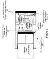
- FIG. 2 is a detailed relational block diagram of an exemplary CF+ card adaptor in accordance with an embodiment of the invention.
- the present invention may be found in a system and method to effectively provide conditioned power to an external add-on card that is communicatively connected to a host computer by way of an external adaptor.
- the external adaptor comprises power conditioning circuitry and optional voltage conversion circuitry that facilitates the generation of an improved power source to the external card.
- the external adaptor establishes a secure physical connection of the external card to the host computer, facilitates communication of the external card to the host computer, and provides a power source that meets or exceeds the operating power requirements of the external card.
- the system and method facilitates the use of an external card having a connector that is incompatible with the PC card connector provided by the host computing device.
- aspects of the present invention may allow a portable laptop computer having a PCMCIA connector (a specific type of PC card connector), to connect to and adequately power a compact flash (CF/CF+) card.
- a portable laptop computer having a PCMCIA connector (a specific type of PC card connector)
- CF/CF+ compact flash
- a user uses the compact flash (CF/CF+) card with an exemplary handheld device such as a pocket PC or PDA.
- the user inserts the compact flash card into the handheld device to increase available memory.
- the external adaptor may facilitate connection of the exemplary laptop to an external card such as a compact flash (CF/CF+) card, secure digital (SD) memory card, PCMCIA card, wireless 802.11 b card, modem card, or any other type of card which may be incompatible to the PC card connector provided by the host computing device.
- CF/CF+ compact flash
- SD secure digital
- aspects of the present invention allow a previously incompatible external card to seamlessly connect to a host computing device, and to properly function by way of using the external adaptor. Aspects of the present invention obviate performance issues that may be related to insufficient power supplied to an external card due to current limitations posed a by host computing device's external card or PC card connector.
- FIG. 1 is a relational block diagram of a system comprising an external card adapter in accordance with an embodiment of the invention.
- the external card adapter comprises an adaptor frame 100, a mating connector to host computing device 104, an external card connector 108, and a printed circuit board (PCB) 112.
- PCB printed circuit board
- an external card (which is not part of the system) is partially inserted into the external card adapter, in order to illustrate the external card adapter.'s mechanism of operation.
- the adaptor frame 100 may comprise a material such as a plastic, that is compatible with any environmental condition generated by a host computing device.
- the adapter frame 100 firmly houses or secures the PCB 112, the mating connector to host computing device 104, and the external card connector 108 together.
- the external card adapter connects to the host computing device's external card connector by way of its mating connector to host computing device 104.
- an external card may be inserted into a recess of the adaptor frame 100, as shown in Figure 1, and connected to the external card by way of the external card connector 108.
- the external card connector 108 may comprise one of many connectors configured for mating with one or more types of external cards.
- one or more connecting pins residing within the external card connector 108 may be reconfigured to mate with the one or more types of external cards.
- the one or more types of external cards may be characterized by different form factors and pin layouts.
- the host computing device mating connector 104 and the external card connector 108 may comprise a number of conductive connecting pins seated within their respective connectors.
- the host computing device mating connector 104 may comprise any type of mating connector compatible to the connector provided by the host computing device.
- the printed circuit board 112 may comprise a mapping circuitry that connects corresponding signals between the external card and the host computing device.
- the circuitry may comprise electrically conductive traces on a PCB that maps corresponding pins of the two connectors 104, 108.
- the printed circuit board 112 comprises a power conditioning circuitry used to condition one or more power signals provided by the host computing device.
- the power signals may be characterized as voltages that are capable of supplying a specified amount of current.
- the power conditioning provided by the power conditioning circuitry generates conditioned power signals to the external card that will satisfy its power requirements.
- the power conditioning circuitry may, for example, provide the external card with a power source that exceeds the external card's instantaneous power requirements.
- the power conditioning circuitry may be selectively enabled by way of a switch positioned on the external card adapter.
- the printed circuit board 112 may intelligently sense that the power delivered to the external card is insufficient for normal operation. As a consequence, electrical components within the printed circuit board 112 may enable or activate the power conditioning circuitry.
- the printed circuit board 112 may comprise electrical components capable of sensing an inadequacy of power delivered to the external card, thereby effectuating a particular voltage in a control signal that may enable the power conditioning circuitry.
- the external card adaptor may be configured to generate an indication, such as by way of illuminating an LED, when the power conditioning circuitry is enabled.
- the power conditioning circuitry comprises any intelligent circuitry capable of effectuating the delivery of conditioned power signals to the external card by the host computing device, by way of the host computing device mating connector 104.
- the power conditioning circuitry may comprise any number of electrical components configured in a way to effectively clean, stabilize, or filter the power signals delivered to the external card.
- the power conditioning circuitry may comprise passive components such as capacitors and/or resistors.
- the power conditioning circuitry may employ bypass capacitors or other low pass filters in order to provide an improved direct current power source to the external card.
- the printed circuit board 112 may contain a voltage conversion circuitry.
- the voltage conversion circuitry may optionally up-convert and/or down-convert voltages in order to supply the appropriate levels of power supply voltages to an external card.
- the voltage conversion circuitry may optionally up-convert voltage levels within the external card adaptor in order to facilitate storage of maximum power within the external card adaptor.
- the voltage conversion circuitry may facilitate a voltage up-conversion of the power supply voltages received by the mating connector to host computing device 104.
- one or more capacitors located within the power conditioning circuitry may store increased charge.
- the increased charge will be used to power the external card that is attached to the external card adaptor.
- the voltage conversion circuitry may be used to facilitate the transfer of power from the external card adaptor to the external card by way of the external card connector 108. As a result of these techniques, an adequate amount of power is capable of being delivered to the external card. Additional details regarding the power conditioning circuitry and voltage converter will be discussed in relation to Figure 2.
- FIG. 2 is a detailed relational block diagram of an exemplary CF+ card adaptor in accordance with an embodiment of the invention.
- the external card that connects to the CF+ card adaptor comprises an exemplary CF+ card while the host computer provides a PCMCIA connector.
- the CF+ card adaptor comprises a CF+ card adaptor frame 200, a mating connector to host computing device 204 (i.e., a mating connector to the host computing device's PCMCIA card connector), a CF+ connector 208, a printed circuit board (PCB) 212, a power conditioning circuitry 216, and a voltage conversion circuitry 220.
- PCB printed circuit board
- the power conditioning circuitry 216 and the voltage conversion circuitry 220 may be implemented on the printed circuit board (PCB) 212.
- the PCB 212 may intelligently sense that the power delivered to the CF+ card is insufficient for proper operation. As a consequence, electrical components within the printed circuit board 212 may enable or activate the power conditioning circuitry.
- the printed circuit board 212 may comprise electrical components capable of sensing an inadequacy of power delivered to the external card, thereby effectuating a certain voltage level (such as a digital 0 or 1) of a control signal that may be used to enable the power conditioning circuitry.
- the CF+ card adapter may comprise a mapping circuitry that appropriately maps corresponding signals between the CF+ card and the host computing device.
- the circuitry may comprise electrically conductive traces on a PCB that maps corresponding signals between the two connectors 204, 208.
- the exemplary CF+ card slides into a suitable recess provided by the CF+ card adapter frame 200, guiding the CF+ card into the CF+ card connector 208.
- one or more conductive Vcc power supply paths 224 originating from the mating connector to host computing device 204 and terminating at the power conditioning circuitry 216. These Vcc power supply paths 224 receive power provided by the host computing device.
- a conditioned Vcc power supply path 228 distributes conditioned power from the voltage conversion circuitry 220 to the CF+ connector.
- the conditioned Vcc power supply path 228 may provide power signals that have been processed by the power conditioning circuitry 216 and the voltage conversion circuitry 220. As shown, the Vcc power may be distributed from the power conditioning circuitry 216 to the voltage conversion circuitry 220. For example, the Vcc power delivered from the host through the mating connector 204 may supply the voltage conversion circuitry 220 by way of the power conditioning circuitry 216. In one embodiment, the voltage conversion circuitry 220 effects a voltage conversion of the voltage supplied to the power conditioning circuitry 216 by way of one or more conductive paths provided by the power conditioning circuitry 216 to the voltage conversion circuitry 220.
- the voltage conversion comprises a voltage up-conversion to facilitate an increased charge to be stored in one or more capacitors located within the power conditioning circuitry 216.
- the voltage conversion circuitry 220 may up-convert and/or down-convert voltages, as required, in order to maximize the power stored within the PCB 212. As a result, an adequate amount of power reserve is stored within the CF+ card adaptor for eventual delivery to the CF+ card.
- the power conditioning circuitry 216 and the voltage conversion circuitry 220 may be selectively enabled by way of intelligent circuitry residing on the PCB 212.
- the intelligent circuitry may comprise a voltage level sensor that monitors the power supply voltages delivered to the exemplary CF+ card.
- the voltage level sensor may trigger use of either the power conditioning circuitry 216 or the voltage conversion circuitry 220 when a power supply voltage delivered to the CF+ card reaches an undesirable level.
- a mechanically or electrically controlled switch enables the voltage conversion circuitry 220.
- one or more indicators may be used to indicate when the power conditioning circuitry 216 and/or voltage conversion circuitry 220 are enabled.
- the one or more indicators may comprise LEDs located in the CF+ card adapter, a software generated indicator that is displayed by way of a monitor at the host computing device, or any other electrically induced indicator.
- the voltage conversion circuitry 220 up-converts or down-converts the voltages of power signals within the CF+ card adapter in order to maximize the power stored within the CF+ card adaptor. For example, the voltage conversion circuitry 220 may up-convert the voltages of the power signals in order to capture more power from the host computing device given a maximum current limitation of the connector of the host computing device. Prior to transmitting the power signals to the CF+ card, the voltage conversion circuitry 220 may down-convert the voltage to levels required by the CF+ card.
- the power conditioning circuitry 216 may comprise any number of electrical components configured in a way to effectively clean, stabilize, or filter the power signals delivered to the exemplary CF+ card.
- the power conditioning circuitry 216 may comprise passive components such as capacitors and/or resistors.
- the power conditioning circuitry 216 may comprise one or more "super" capacitors that act as reservoirs of charge. These large capacitors provide a stable source of power to the CF+ card during transient or instantaneous power surge occurrences.
- bypass capacitors may be used at various points along the PCB 212 to filter out noise that may be present in the power supply signals provided by the host computing device.
- FIG. 2 describes a CF+ card adapter
- other types of external cards may be adapted for use by the present invention.
- the circuitry residing on the PCB may be appropriately configured for use with external cards of different form factors and power requirements.
- the signal conduction paths and electrical components of the printed circuit board (PCB), the power conditioning circuitry, and voltage conversion circuitry, as previously described in the preceding embodiments may be configured to satisfy the operational requirements of the external card used.
Landscapes
- Engineering & Computer Science (AREA)
- Physics & Mathematics (AREA)
- General Physics & Mathematics (AREA)
- Theoretical Computer Science (AREA)
- Computer Hardware Design (AREA)
- Microelectronics & Electronic Packaging (AREA)
- Artificial Intelligence (AREA)
- Computer Vision & Pattern Recognition (AREA)
- Power Sources (AREA)
Abstract
Description
Claims (10)
- A method of providing conditioned power signals from an external card adaptor to an external card comprising:receiving one or more power signal inputs from a host computing device; andconditioning said one or more power signal inputs to generate said conditioned power signals.
- The method of Claim 1 further comprising transmitting said conditioned power signals to said external card adaptor.
- The method of Claim 1 or 2 further comprising performing voltage conversion of said one or more power signal inputs.
- The method of Claim 3 wherein said voltage conversion up-converts one or more voltages of said one or more power signals inputs to increase power stored within the external card adaptor.
- The method of Claim 3 or 4 wherein said voltage conversion up-converts or down-converts one or more voltages of said one or more power signal inputs in order to deliver appropriate voltage levels to said external card.
- A method of supplying power to an external card that is communicatively connected to a host computing device by way of an adaptor. comprising:receiving one or more input power signals from said host computing device by said adaptor;converting one or more voltages of said one or more input power signals in order to increase power stored in said adaptor; andconditioning said one or more input power signals.
- The method of claim 6 wherein conditioning said one or more power signal inputs comprises filtering said one or more power signal inputs using one or more passive electrical components to eliminate noise.
- A system for providing conditioned power signals from an external card adaptor to an external card comprising:a first connector for connecting said external card adaptor to said external card;a second connector for connecting said external card adaptor to a host computing device;a printed circuit board capable of implementing power conditioning functions; andan adaptor frame used for receiving said external card and securing said first connector, said second connector, and said printer circuit board.
- The system of Claim 8 wherein said printed circuit board comprises a mapping circuitry that appropriately maps corresponding signals between said external card and said host computing device.
- The system of Claim 8 or 9 further comprising a power conditioning circuitry used to condition one or more power supply signals provided by said host computing device.
Applications Claiming Priority (4)
| Application Number | Priority Date | Filing Date | Title |
|---|---|---|---|
| US50588103P | 2003-09-24 | 2003-09-24 | |
| US505881P | 2003-09-24 | ||
| US10/679,095 US7155620B2 (en) | 2003-09-24 | 2003-10-03 | Power conditioning mechanism using an external card adapter |
| US679095 | 2003-10-03 |
Publications (2)
| Publication Number | Publication Date |
|---|---|
| EP1519308A2 true EP1519308A2 (en) | 2005-03-30 |
| EP1519308A3 EP1519308A3 (en) | 2009-02-18 |
Family
ID=34198321
Family Applications (1)
| Application Number | Title | Priority Date | Filing Date |
|---|---|---|---|
| EP04018122A Withdrawn EP1519308A3 (en) | 2003-09-24 | 2004-07-30 | Power conditioning mechanism using an external card adapter |
Country Status (2)
| Country | Link |
|---|---|
| US (1) | US7155620B2 (en) |
| EP (1) | EP1519308A3 (en) |
Cited By (1)
| Publication number | Priority date | Publication date | Assignee | Title |
|---|---|---|---|---|
| EP2411919A4 (en) * | 2009-03-26 | 2013-09-11 | Sierra Wireless Inc | METHOD AND APPARATUS FOR CONTROLLING THE OPERATING CONDITIONS OF A PERIPHERAL DEVICE BASED ON AN INTERCONNECTION MODE |
Families Citing this family (7)
| Publication number | Priority date | Publication date | Assignee | Title |
|---|---|---|---|---|
| EP1648152A1 (en) * | 2004-10-14 | 2006-04-19 | Thomson Multimedia Broadband Belgium | Integrated access device, associated modem box and splitting module |
| US20060146463A1 (en) * | 2005-01-04 | 2006-07-06 | Demian Martin | In-wall power system and method |
| US9405339B1 (en) * | 2007-04-30 | 2016-08-02 | Hewlett Packard Enterprise Development Lp | Power controller |
| KR101933431B1 (en) * | 2012-04-19 | 2018-12-31 | 삼성전자주식회사 | Device and method for controlling power of external memory in wireless terminal |
| US11250307B2 (en) | 2017-03-23 | 2022-02-15 | Idex Biometrics Asa | Secure, remote biometric enrollment |
| US10282651B2 (en) * | 2017-03-23 | 2019-05-07 | Idex Asa | Sensor array system selectively configurable as a fingerprint sensor or data entry device |
| WO2019116233A1 (en) | 2017-12-12 | 2019-06-20 | Idex Asa | Power source for biometric enrollment with status indicators |
Family Cites Families (15)
| Publication number | Priority date | Publication date | Assignee | Title |
|---|---|---|---|---|
| CA2092486C (en) * | 1992-05-11 | 1999-05-11 | Vincent Ferri | Automatic slot identification and address decoding system |
| US5887145A (en) * | 1993-09-01 | 1999-03-23 | Sandisk Corporation | Removable mother/daughter peripheral card |
| US6329856B1 (en) * | 2000-08-28 | 2001-12-11 | Summit Microelectronics, Inc. | Method and apparatus for tracking and controlling voltage and current transitions |
| FR2821988A1 (en) * | 2001-03-09 | 2002-09-13 | Itt Mfg Enterprises Inc | ELECTRICAL CONNECTOR FOR ELECTRONIC MEMORY CARDS WITH LARGE STORAGE CAPACITY |
| US20020178307A1 (en) * | 2001-05-25 | 2002-11-28 | Pua Khein Seng | Multiple memory card adapter |
| JP2003099394A (en) * | 2001-09-26 | 2003-04-04 | Murata Mfg Co Ltd | Interface card for media card |
| US7136950B2 (en) * | 2001-10-02 | 2006-11-14 | Texas Instruments Incorporated | Multifunction passive adaptor for flash media cards |
| US7375647B2 (en) * | 2001-10-15 | 2008-05-20 | Imetrikus, Inc. | Method and apparatus for communicating data between a medical device and a central data repository |
| TW515940B (en) * | 2001-11-23 | 2003-01-01 | Compal Electronics Inc | Add-on card for wireless communication with power managing circuit |
| US6892167B2 (en) * | 2001-11-28 | 2005-05-10 | Sypris Data Systems, Inc. | Real-time data acquisition and storage network |
| US6904531B2 (en) * | 2002-02-05 | 2005-06-07 | Mitac Technology Corp. | Portable computer with low power consumption of a card bus controller thereof |
| US6606251B1 (en) * | 2002-02-07 | 2003-08-12 | Cooligy Inc. | Power conditioning module |
| US20040103223A1 (en) * | 2002-11-26 | 2004-05-27 | Motorola, Inc. | USB accessory adaptor |
| US20040192114A1 (en) * | 2003-03-27 | 2004-09-30 | Han-Sen Liou | Multi-signal transferred connector |
| US6970964B2 (en) * | 2003-03-28 | 2005-11-29 | Texas Instruments Incorporated | Using PCMCIA/PCI drivers to control USB ports |
-
2003
- 2003-10-03 US US10/679,095 patent/US7155620B2/en not_active Expired - Lifetime
-
2004
- 2004-07-30 EP EP04018122A patent/EP1519308A3/en not_active Withdrawn
Cited By (1)
| Publication number | Priority date | Publication date | Assignee | Title |
|---|---|---|---|---|
| EP2411919A4 (en) * | 2009-03-26 | 2013-09-11 | Sierra Wireless Inc | METHOD AND APPARATUS FOR CONTROLLING THE OPERATING CONDITIONS OF A PERIPHERAL DEVICE BASED ON AN INTERCONNECTION MODE |
Also Published As
| Publication number | Publication date |
|---|---|
| EP1519308A3 (en) | 2009-02-18 |
| US20050066071A1 (en) | 2005-03-24 |
| US7155620B2 (en) | 2006-12-26 |
Similar Documents
| Publication | Publication Date | Title |
|---|---|---|
| US20070126290A1 (en) | Systems and methods for powering an electronic device from selectable power sources | |
| JP2003263245A (en) | USB device | |
| US6844846B1 (en) | Multi-mode GPS receiver | |
| EP1198049A1 (en) | Charging circuit for charging a mobile terminal through an USB interface | |
| WO2005013456A1 (en) | Data cable for detecting power source automatically | |
| US7155620B2 (en) | Power conditioning mechanism using an external card adapter | |
| US20080012524A1 (en) | Chargeable electronic devices and direct current voltage supply systems | |
| CN102929821A (en) | Electronic device and electronic device system | |
| US20040059860A1 (en) | Double-interface adaptor for memory cards | |
| US20110047393A1 (en) | External Device Charging While Notebook Is Off | |
| EP0855281A3 (en) | Portable printer with interface for receiving supply of power from external source | |
| JP2003272582A (en) | Card-type battery device and electronic apparatus using the same | |
| EP1235157A2 (en) | Peripheral with expansion connector attachable to host | |
| EP0656600A3 (en) | An information processing system using portable terminal unit and data communication adapter therefor | |
| US20060243801A1 (en) | PC card device with express card | |
| CN209388295U (en) | A kind of usb circuit and electronic equipment for realizing while charging and powering | |
| US20230166622A1 (en) | Multi-purpose charger | |
| CN116610616A (en) | Conversion circuit and communication device | |
| CN210577869U (en) | Charging and power conversion circuit and connector thereof | |
| CN205264965U (en) | On -vehicle USBSD concentrator | |
| CN211585188U (en) | Wireless adapter for gamepad and gamepad | |
| US10754805B1 (en) | USB adapter | |
| US20090240863A1 (en) | Distributed power regulation | |
| CN208156199U (en) | positioning and communication system based on SIM868 | |
| CN210015472U (en) | Multifunctional integrated lottery terminal |
Legal Events
| Date | Code | Title | Description |
|---|---|---|---|
| PUAI | Public reference made under article 153(3) epc to a published international application that has entered the european phase |
Free format text: ORIGINAL CODE: 0009012 |
|
| AK | Designated contracting states |
Kind code of ref document: A2 Designated state(s): AT BE BG CH CY CZ DE DK EE ES FI FR GB GR HU IE IT LI LU MC NL PL PT RO SE SI SK TR |
|
| AX | Request for extension of the european patent |
Extension state: AL HR LT LV MK |
|
| RAP1 | Party data changed (applicant data changed or rights of an application transferred) |
Owner name: BROADCOM CORPORATION |
|
| PUAL | Search report despatched |
Free format text: ORIGINAL CODE: 0009013 |
|
| AK | Designated contracting states |
Kind code of ref document: A3 Designated state(s): AT BE BG CH CY CZ DE DK EE ES FI FR GB GR HU IE IT LI LU MC NL PL PT RO SE SI SK TR |
|
| AX | Request for extension of the european patent |
Extension state: AL HR LT LV MK |
|
| 17P | Request for examination filed |
Effective date: 20090818 |
|
| 17Q | First examination report despatched |
Effective date: 20090907 |
|
| AKX | Designation fees paid |
Designated state(s): DE FR GB |
|
| STAA | Information on the status of an ep patent application or granted ep patent |
Free format text: STATUS: THE APPLICATION IS DEEMED TO BE WITHDRAWN |
|
| 18D | Application deemed to be withdrawn |
Effective date: 20140201 |