EP1517593A2 - Method and apparatus for a voltage controlled start-up circuit for an electronic ballast - Google Patents
Method and apparatus for a voltage controlled start-up circuit for an electronic ballast Download PDFInfo
- Publication number
- EP1517593A2 EP1517593A2 EP04255757A EP04255757A EP1517593A2 EP 1517593 A2 EP1517593 A2 EP 1517593A2 EP 04255757 A EP04255757 A EP 04255757A EP 04255757 A EP04255757 A EP 04255757A EP 1517593 A2 EP1517593 A2 EP 1517593A2
- Authority
- EP
- European Patent Office
- Prior art keywords
- voltage
- lamp
- starting circuit
- circuit
- set forth
- Prior art date
- Legal status (The legal status is an assumption and is not a legal conclusion. Google has not performed a legal analysis and makes no representation as to the accuracy of the status listed.)
- Ceased
Links
- 238000000034 method Methods 0.000 title claims description 9
- 238000010304 firing Methods 0.000 claims abstract description 12
- 230000001934 delay Effects 0.000 claims abstract description 5
- 239000003990 capacitor Substances 0.000 claims description 44
- 230000015556 catabolic process Effects 0.000 claims description 17
- 238000012937 correction Methods 0.000 claims description 11
- 230000005669 field effect Effects 0.000 claims description 2
- 238000004804 winding Methods 0.000 description 9
- 230000010355 oscillation Effects 0.000 description 5
- 230000001419 dependent effect Effects 0.000 description 4
- 238000013461 design Methods 0.000 description 4
- 230000001939 inductive effect Effects 0.000 description 4
- 230000008878 coupling Effects 0.000 description 3
- 238000010168 coupling process Methods 0.000 description 3
- 238000005859 coupling reaction Methods 0.000 description 3
- 238000010586 diagram Methods 0.000 description 3
- 230000000694 effects Effects 0.000 description 3
- 230000007704 transition Effects 0.000 description 3
- 238000006842 Henry reaction Methods 0.000 description 2
- 230000008901 benefit Effects 0.000 description 2
- 230000001052 transient effect Effects 0.000 description 2
- 230000009471 action Effects 0.000 description 1
- 238000013459 approach Methods 0.000 description 1
- 230000008859 change Effects 0.000 description 1
- 238000011161 development Methods 0.000 description 1
- 238000007599 discharging Methods 0.000 description 1
- 230000003628 erosive effect Effects 0.000 description 1
- 230000002441 reversible effect Effects 0.000 description 1
- 230000036962 time dependent Effects 0.000 description 1
- 230000001960 triggered effect Effects 0.000 description 1
Images



Classifications
-
- H—ELECTRICITY
- H05—ELECTRIC TECHNIQUES NOT OTHERWISE PROVIDED FOR
- H05B—ELECTRIC HEATING; ELECTRIC LIGHT SOURCES NOT OTHERWISE PROVIDED FOR; CIRCUIT ARRANGEMENTS FOR ELECTRIC LIGHT SOURCES, IN GENERAL
- H05B41/00—Circuit arrangements or apparatus for igniting or operating discharge lamps
- H05B41/14—Circuit arrangements
- H05B41/26—Circuit arrangements in which the lamp is fed by power derived from DC by means of a converter, e.g. by high-voltage DC
- H05B41/28—Circuit arrangements in which the lamp is fed by power derived from DC by means of a converter, e.g. by high-voltage DC using static converters
- H05B41/282—Circuit arrangements in which the lamp is fed by power derived from DC by means of a converter, e.g. by high-voltage DC using static converters with semiconductor devices
- H05B41/2825—Circuit arrangements in which the lamp is fed by power derived from DC by means of a converter, e.g. by high-voltage DC using static converters with semiconductor devices by means of a bridge converter in the final stage
-
- Y—GENERAL TAGGING OF NEW TECHNOLOGICAL DEVELOPMENTS; GENERAL TAGGING OF CROSS-SECTIONAL TECHNOLOGIES SPANNING OVER SEVERAL SECTIONS OF THE IPC; TECHNICAL SUBJECTS COVERED BY FORMER USPC CROSS-REFERENCE ART COLLECTIONS [XRACs] AND DIGESTS
- Y10—TECHNICAL SUBJECTS COVERED BY FORMER USPC
- Y10S—TECHNICAL SUBJECTS COVERED BY FORMER USPC CROSS-REFERENCE ART COLLECTIONS [XRACs] AND DIGESTS
- Y10S315/00—Electric lamp and discharge devices: systems
- Y10S315/07—Starting and control circuits for gas discharge lamp using transistors
Definitions
- the present application relates to ballasts, and power supply circuits for gas discharge lamps. It finds particular application for use with current fed instant and/or rapid start electronic ballasts or power supply circuits and will be described with particular reference thereto. It is to be appreciated, however, that the present application is also applicable to other inverter circuits, and is not limited to the aforementioned use.
- active pre-regulators While the use of active pre-regulators has provided improved performance in certain areas, new problems have arisen when these pre-regulators are put into operation with rapid and/or instant-start ballasts or power supply circuits. Particularly, systems employing active pre-regulators require a significant amount of time to reach steady state operating conditions during start-up. This may result in undesirable operating conditions for the gas discharge lamps when the less than steady state operating voltages are passed through the converter section during this transient start-up condition.
- the active pre-regulator will provide a pre-determined DC voltage output, whose value will be dependent on the circuit design and/or lamp being driven, but in many instances may be up to a 500 V DC output.
- the output will be substantially below the desired steady state voltage conditions. Therefore, when operating in rapid and instant start modes the voltage supply will not be at steady state, and may result in an undesirable effect of unacceptable "preheat" or glow periods at this lower voltage.
- Instant-start lamps are typically specified to be operated in a glow discharge mode for a very short time period, approximately for no more than 100 milliseconds. This is a requirement since longer "preheat" periods will act to shorten lamp life due to excessive electrode erosion during these glow discharge conditions.
- ballasts or power supply circuits having universal input capabilities have become a key selling point.
- a device is considered a universal input device if it is capable of operating cooperatively with the various standardized line voltages supplied in different parts of the world.
- the standard line voltage in the United States is 120 V, in China it is 220 V, and in Europe, 230 V.
- a universal device would also preferably be able to operate with industrial line voltages which is currently 277 V in the United States.
- a lamp inverter circuit includes a switching portion that converts a DC signal to an AC signal. Further, the circuit includes an input portion for receiving a line voltage signal, a resonant load portion for receiving a lamp load, and a voltage controlled start-up portion that controls the ignition of the lamp based on a detected voltage.
- a method of firing a lamp is provided.
- An AC line voltage is supplied and converted into a DC bus voltage.
- a charging capacitor is charged by the bus voltage.
- a breakdown voltage of a diac is overcome, turning the diac conductive, supplying current to oscillation of the inverter circuit.
- a lamp ballast in accordance with another aspect of the present application, includes a switching portion that includes first and second bipolar junction transistors.
- the ballast also includes a resonant load portion for receiving a lamp, a power factor correction circuit for delivering a bus voltage, and a voltage dependent start-up portion that controls firing of the lamp until the bus voltage ramps up to a pre-determined threshold.
- lamp circuit A includes a lamp assembly 10 operably connected to a bus voltage sensing and self-oscillating inverter/starting circuit 12.
- the lamp assembly 10 can be a gas discharge lamp or a plurality of gas discharge lamps, such as linear fluorescent or compact fluorescent lamps that operate at a particular frequency or range of frequencies.
- the inverter starting circuit 12 is connected to power factor correction (PFC) circuit 14, such as an active power factor correction circuit which regulates a line voltage, corrects harmonics and supplies a bus voltage to inverter starting circuit 12.
- PFC circuit 14 may provide passive power correction in an alternate embodiment.
- An AC voltage source 16 supplies an alternating current signal to the PFC circuit 14.
- the voltage source 16 can deliver a wide range of signals.
- the standard wall socket delivers a 120 V RMS voltage.
- the standard line voltage in China is 220 V, and Europe is higher, at about 230 V.
- Other sources, such as ones used for more industrial applications can deliver voltages of 277 V or higher.
- the resulting bus voltages produced by PFC 14 range from 169 V (with a 120 V input) to 390 V (with a 277 V input), or more.
- the PFC circuit 14 can accept an input line voltage in the above disclosed range, in addition to accommodating higher or lower input voltages. Active and/or passive power factor correction circuits of this type are well known in the art, and therefore a detailed description of their operation is not undertaken here.
- FIGURE 2 illustrated is a detailed view of the inverter starting circuit 12 in a current fed half bridge inverter implementation.
- a first transistor 20 and a second transistor 22 alternate between periods of conductivity and periods of non-conductivity, out of phase with each other. That is, when the first transistor 20 is conductive, the second transistor 22 is non-conductive, and vice-versa.
- the transistors 20, 22 are part of a switching portion of the inverter circuit 12. The action of alternating periods of conduction of the transistors provides an AC signal to the lamp assembly 10.
- the transistors are bipolar junction transistors (BJTs), but it is to be understood the concepts of the present application may be incorporated in other inverter circuits, such as known in the art. For example, the following descriptions may be implemented with BJTs in both half-wave current fed ballasts and push-pull type current fed electronic ballasts, among others.
- BJTs bipolar junction transistors
- each transistor 20, 22 has a respective base, (B) emitter, (E) and collector (C).
- the voltage from base to emitter on either transistor defines the conduction state of that transistor. That is, the base to emitter voltage of transistor 20 defines the conductivity of transistor 20 and the base to emitter voltage of transistor 22 defines the conductivity of transistor 22.
- neither of the transistors 20, 22 are conductive when current is initially supplied by the PFC circuit 14 to the inverter starting circuit 12.
- a start-up portion 24 of the inverter circuit prevents current from being supplied to the transistors 20, 22 before the bus voltage from the PFC circuit 14 reaches a predetermined threshold voltage.
- the start-up portion includes Zener diode 26, diode 28, capacitor 30, and diac 32.
- capacitors 34 and 36 are of equal value, so that the voltage across capacitor 34 is the same as the voltage across capacitor 36.
- resistors 38, 40, and 42 are resistors 38, 40, and 42. Resistors 38 and 40 form a voltage divider at node 44 and current is supplied to the start-up portion 24 through voltage divider 38, 40.
- Zener diode 26 and diode 28 prevent any significant current from passing through start-up portion 24.
- a portion of the circuit current charges capacitors 34 and 36, other current charges snubber capacitor 46, and the remaining current flows through resistors 38, 40, and 42.
- a breakdown voltage of Zener diode 26 is not reached, and Zener diode 26 prevents current from passing through start-up portion 24.
- the bus voltage from PFC 14 ramps to a level where the potential at node 44 is greater than the breakdown voltage of Zener diode 26 turning Zener diode 26 conductive, supplying increased current levels to start-up portion 24, and more specifically, to capacitor 30.
- the breakdown voltage of Zener diode 26 is between 64.5 and 71.5 V, and preferably 68 V.
- Zener diode 26 turns conductive (from left to right in FIG. 2) capacitor 30 begins charging. At this point, current is being supplied to start-up portion 24, but diac 32 prevents the base of transistor 20 from becoming conductive in the collector-emitter direction. As the bus voltage continues ramping up, capacitor 30 collects more charge, and eventually reaches a potential to overcome the breakover voltage of diac 32. When the breakover voltage is reached, transistor 20 turns conductive, wherein inverter starting circuit 12 begins to oscillate, and after approximately 0.7 seconds, lamp assembly 10 is ignited.
- capacitor 30 no longer has an opportunity to continuously collect charge. Current flows directly from node 44 to capacitor 30, since transistor 20 is conductive after diac 32 breaks down. Diode 28 provides a path to allow capacitor 30 to discharge, once per cycle.
- the inverter starting circuit 12 now operates as is typical, with no further activity from the start-up portion 24.
- switching transistors 20, 22 are driven by respective drive circuits 48, 50.
- Drive circuit 48 incorporates diode 52, resistor 54 combination supplied via coupling of winding 58.
- Drive circuit 50 incorporates diode 60, resistor 62 combination, supplied via coupling of windings 66.
- Lamp assembly 10 is provided with power from inverter starting circuit 12 by a coupling between windings 68 and 70, where winding 70 has a capacitor 72 across its primary winding and are considered resonant load components.
- breakover voltage of diac 32 is chosen to be an optimal bus voltage for starting the inverter circuit and ignition voltage of lamp assembly 10.
- the breakover voltage of diac 32 is chosen to be such that when the bus voltage (the voltage across capacitors 34 and 36) reaches a pre-determined value, for example about 390 V, diac 32 reaches its breakover voltage.
- start-up portion 24 detects when the bus voltage reaches the preferred firing voltage by virtue of the chosen breakover voltage of diac 32.
- the breakover voltage of the diac 32 is between 20 V and 40 V, and preferably about 32 V.
- first transistor 20 is also applicable to second transistor 22. That is, as shown in FIGURE 3 in an alternate inverter starting circuit 12' embodiment, the start-up portion 24 is connected to second transistor 22, and it, instead of first transistor 20, would initiate oscillations. Components having similar operation and use as components in FIGURE 2 are similarly numbered as in FIGURE 2.
- the firing voltage is chosen to be about 300 V or greater for rapid start ballasts.
- FIGURE 4a provides a graphed time sequence of a rapid start electronic ballast incorporating inverter starting circuit 12 of the present application.
- the sequence includes three distinct transitions.
- Fo a 120 V input line, from turn-on (0) to to the bus voltage transitions from its starting voltage (e.g. 169 V) to a preferred pre-heat voltage (e.g. 390 V).
- the time duration to t 0 -t 1 is a pre-heat time (e.g. steady 390 V), and from t 1 to t 2 , the bus voltage ramps up to its steady state (e.g. 500 V).
- FIGURE 4b depicted is a chart showing inverter starting time for a rapid start electronic ballast incorporating inverter starting circuit 12.
- FIGURE 4b illustrates the voltage dependency of the circuit, and emphasizes that operation to start the circuit is not a time dependent factor but is rather a voltage controlled concept. There is no pre-determined time following energization that the oscillations will begin.
- the starting of the circuit is controlled by the value of the bus voltage.
- FIGURE 5 depicted is operation of charge capacitor 30 of FIGURE 2, which illustrates its two distinct charging rates.
- Charge capacitor 30 will always have an amount of stored energy to be used for the breakover of diac 32.
- capacitor 30 charges at a very quick rate, and when below 300 V bus voltage, capacitor 30 is being charged only due to leakage current.
- Zener diode 26 never turns conductive in its reverse direction, and allows only a leakage current 80 to charge capacitor 30. After the bus voltage reaches 300 V, a significantly higher charging current 82 is available to capacitor 30.
- the starting bus voltage is the starting bus voltage. For a 120 V line input, the output bus voltage ramps up from about 169 V. For a 277 V line input, the output bus voltage ramps up from about 390 V. As stated earlier, the start time (FIGURE 4b) is about 40 milliseconds at 390 V.
- one exemplary firing voltage is 390 V, because it is greater than the 300 V required for mode transition, is less than common steady state operating voltages, and fires the lamp as soon as possible, before the bus voltage reaches steady state.
- greater or lesser firing voltages can be chosen, for example in some applications the bus voltage may experience an overshoot during start-up, based on known line voltages and desired universality of the inverter.
- FIGURES 2 and 3 are two implementations of a new starting circuit in conjunction with a current fed, half-bridge inverter circuit.
- the main bus voltage is sensed by a three resistor divider circuit. A portion of the bus voltage is applied to a Zener diode and a charging capacitor. When the voltage reaches a pre-determined level, the Zener diode breaks down, allowing the charging capacitor to charge. A diac then breaks down, causing the self-oscillating inverter to be triggered. A diode prevents the charging capacitor from charging, allowing it to discharge every half-cycle, when a first transistor is on.
- the component values are selected such that the Zener breakdown voltage is at least double the diac breakdown voltage, or higher. Possible applications of the present invention include General Electric's 4 ft. and 8 ft. T12 and T8 electronic lamp ballasts.
- Exemplary component values for the circuits of FIGURES 2 and 3 are as follows: Part Description Part Number Nominal Value Lamp Assembly 10 40 Watts Line Voltage 16 120-277 Volts First Transistor 20 BJT SPB 11 NM60 Second Transistor 22 BJT SPB 11 NM60 Bus Capacitor 34 33 ⁇ f Bus Capacitor 36 33 ⁇ f Bus Resistor 38 400 k ⁇ Bus Resistor 40 620 k ⁇ Bus Resistor 42 1 M ⁇ Zener Diode 26 68 V Diode 28 UF 4007 Capacitor 46 1.2 nf Charging Capacitor 30 0.1 ⁇ f Diac 32 HT-32 Zener Diode 74 P6KE440A Zener Diode 76 P6KE440A Inductive Winding 56 5 mh Inductive Winding 64 5 mh Base Diode 52 1N5817 Base Diode 60 1N5817 Base Resistor 54 75 ⁇ Base Resistor 62 75 ⁇ Inductive Winding 70 0.85 Henries Inductive Winding
Landscapes
- Circuit Arrangements For Discharge Lamps (AREA)
- Inverter Devices (AREA)
Abstract
Description
- The present application relates to ballasts, and power supply circuits for gas discharge lamps. It finds particular application for use with current fed instant and/or rapid start electronic ballasts or power supply circuits and will be described with particular reference thereto. It is to be appreciated, however, that the present application is also applicable to other inverter circuits, and is not limited to the aforementioned use.
- In the late eighties, and early nineties, the lighting industry began to make a shift from passive power and harmonic correction circuits to active power correction and harmonic circuits in the form of active pre-regulators for use in conjunction with electronic lamp ballasts. An advantage of active power factor and harmonic correction via active pre-regulators is that bus voltage variation can be virtually eliminated even though there are still voltage variations on the input line. The visible effect of this change is less variation in lumen output, that is, lamps connected to active pre-regulator circuits exhibit steadier intensities than lamps connected to circuits without active pre-regulation.
- While the use of active pre-regulators has provided improved performance in certain areas, new problems have arisen when these pre-regulators are put into operation with rapid and/or instant-start ballasts or power supply circuits. Particularly, systems employing active pre-regulators require a significant amount of time to reach steady state operating conditions during start-up. This may result in undesirable operating conditions for the gas discharge lamps when the less than steady state operating voltages are passed through the converter section during this transient start-up condition.
- During normal operation, which is a steady state condition, the active pre-regulator will provide a pre-determined DC voltage output, whose value will be dependent on the circuit design and/or lamp being driven, but in many instances may be up to a 500 V DC output. During the transient start-up condition, the output will be substantially below the desired steady state voltage conditions. Therefore, when operating in rapid and instant start modes the voltage supply will not be at steady state, and may result in an undesirable effect of unacceptable "preheat" or glow periods at this lower voltage. Instant-start lamps are typically specified to be operated in a glow discharge mode for a very short time period, approximately for no more than 100 milliseconds. This is a requirement since longer "preheat" periods will act to shorten lamp life due to excessive electrode erosion during these glow discharge conditions. Additionally, when operating in low voltage (i.e. non-steady state conditions), undesirable visible phenomena such as lamp flickering may occur. Therefore, it is considered desirable to delay the start-up operation of an electronic ballast for instant-start type fluorescent lamps until a pre-determined DC bus voltage has been substantially reached.
- One particular attempt to address this issue is set forth in US patent 5,177,408 to Marques which issued January 5, 1993. This patent disclosed a time delay circuit of an electronic ballast for "instant-start" type fluorescent lamps of the type having an electronic converter powered by an active electronic pre-regulator. The inverter is described as an inductive-capacitive parallel-resonant push-pull circuit or other type of current-fed power-resonant circuit. The start-up circuit may be either a resistor and Zener diode or a resistor, capacitor, and diac network programmable uni-junction transistor circuit connected between the pre-regulator output and an oscillation-enabling input of the inverter. The active electronic pre-regulator is designed so that it takes a pre-determined start-up time to reach steady state operating conditions. This delay device is connected between the pre-regulator and the converter.
- Drawbacks to the above disclosed design exist. For example, to minimize design and development cost, to lower the number of different products (i.e. SKUs), to simplify inventory control, and to address global market needs, ballasts or power supply circuits having universal input capabilities have become a key selling point. In theory, a device is considered a universal input device if it is capable of operating cooperatively with the various standardized line voltages supplied in different parts of the world. For example, the standard line voltage in the United States is 120 V, in China it is 220 V, and in Europe, 230 V. A universal device would also preferably be able to operate with industrial line voltages which is currently 277 V in the United States.
- The aforementioned US Patent 5,177,408 is, however, dependent on the input line voltage to obtain its time delay. This means to obtain a pre-determined time delay, it would be necessary to take into consideration the line voltage with which the device will be operating. Such a device would not therefore be considered a universal input ballast or power supply. Particularly, if a unit were used with a 120 V input line, the time delay would be different than if that unit were receiving a 230 V input line. Thus, this approach does not take full advantage of active power factor correction control.
- In accordance with one aspect of the present application, a lamp inverter circuit is provided. The lamp inverter circuit includes a switching portion that converts a DC signal to an AC signal. Further, the circuit includes an input portion for receiving a line voltage signal, a resonant load portion for receiving a lamp load, and a voltage controlled start-up portion that controls the ignition of the lamp based on a detected voltage.
- In accordance with another aspect of the present application, a method of firing a lamp is provided. An AC line voltage is supplied and converted into a DC bus voltage. A charging capacitor is charged by the bus voltage. A breakdown voltage of a diac is overcome, turning the diac conductive, supplying current to oscillation of the inverter circuit.
- In accordance with another aspect of the present application, a lamp ballast is provided. The lamp ballast includes a switching portion that includes first and second bipolar junction transistors. The ballast also includes a resonant load portion for receiving a lamp, a power factor correction circuit for delivering a bus voltage, and a voltage dependent start-up portion that controls firing of the lamp until the bus voltage ramps up to a pre-determined threshold.
- Embodiments of the invention will now be described, by way of example, with reference to the accompanying drawings, in which:
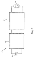
- FIGURE 1 is a block diagram of a lamp system;
- FIGURE 2 is a circuit diagram of ballast inverter circuit included in the lamp system shown in FIGURE 1 with a start up portion operably connected with a high side switch of the inverter circuit;
- FIGURE 3 is a circuit diagram similar to the ballast of FIGURE 2, however the implementation of the start-up portion is on a low side switch of the inverter circuit;
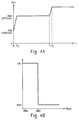
- FIGURE 4a shows the bus voltage over a time sequence for the rapid start electronic ballast according to the present application;
- FIGURE 4b provides a function of the bus voltage versus starting time for a rapid start electronic ballast according to the present application; and
- FIGURE 5 depicts the charge current of
capacitor 30 of FIGURE 2 as a function of the bus voltage. -
- With reference to FIGURE 1, lamp circuit A includes a
lamp assembly 10 operably connected to a bus voltage sensing and self-oscillating inverter/starting circuit 12. Thelamp assembly 10 can be a gas discharge lamp or a plurality of gas discharge lamps, such as linear fluorescent or compact fluorescent lamps that operate at a particular frequency or range of frequencies. In one embodiment, theinverter starting circuit 12 is connected to power factor correction (PFC)circuit 14, such as an active power factor correction circuit which regulates a line voltage, corrects harmonics and supplies a bus voltage to inverterstarting circuit 12. It is to be understood thatPFC circuit 14 may provide passive power correction in an alternate embodiment. AnAC voltage source 16 supplies an alternating current signal to thePFC circuit 14. Thevoltage source 16 can deliver a wide range of signals. Currently in the United States, the standard wall socket delivers a 120 V RMS voltage. The standard line voltage in China is 220 V, and Europe is higher, at about 230 V. Other sources, such as ones used for more industrial applications can deliver voltages of 277 V or higher. In one embodiment, the resulting bus voltages produced byPFC 14 range from 169 V (with a 120 V input) to 390 V (with a 277 V input), or more. ThePFC circuit 14 can accept an input line voltage in the above disclosed range, in addition to accommodating higher or lower input voltages. Active and/or passive power factor correction circuits of this type are well known in the art, and therefore a detailed description of their operation is not undertaken here. - With reference to FIGURE 2, illustrated is a detailed view of the
inverter starting circuit 12 in a current fed half bridge inverter implementation. In order to convert a DC bus signal into an AC signal, afirst transistor 20 and asecond transistor 22 alternate between periods of conductivity and periods of non-conductivity, out of phase with each other. That is, when thefirst transistor 20 is conductive, thesecond transistor 22 is non-conductive, and vice-versa. Thetransistors inverter circuit 12. The action of alternating periods of conduction of the transistors provides an AC signal to thelamp assembly 10. In the embodiment illustrated in FIGURE 2, the transistors are bipolar junction transistors (BJTs), but it is to be understood the concepts of the present application may be incorporated in other inverter circuits, such as known in the art. For example, the following descriptions may be implemented with BJTs in both half-wave current fed ballasts and push-pull type current fed electronic ballasts, among others. - In this embodiment, each
transistor transistor 20 defines the conductivity oftransistor 20 and the base to emitter voltage oftransistor 22 defines the conductivity oftransistor 22. In the illustrated embodiment neither of thetransistors PFC circuit 14 to theinverter starting circuit 12. As will be expanded upon below, a start-upportion 24 of the inverter circuit prevents current from being supplied to thetransistors PFC circuit 14 reaches a predetermined threshold voltage. The start-up portion includesZener diode 26,diode 28,capacitor 30, anddiac 32. - The potential difference across
capacitors PFC circuit 14. In one embodiment,capacitors capacitor 34 is the same as the voltage acrosscapacitor 36. In parallel withcapacitors resistors Resistors node 44 and current is supplied to the start-upportion 24 throughvoltage divider - When power is first applied to the
inverter starting circuit 12,Zener diode 26 anddiode 28 prevent any significant current from passing through start-upportion 24. As the bus voltage ramps up, after power is initially supplied to inverter startingcircuit 12, a portion of the circuitcurrent charges capacitors charges snubber capacitor 46, and the remaining current flows throughresistors resistors Zener diode 26 is not reached, andZener diode 26 prevents current from passing through start-upportion 24. Eventually, the bus voltage fromPFC 14 ramps to a level where the potential atnode 44 is greater than the breakdown voltage ofZener diode 26 turningZener diode 26 conductive, supplying increased current levels to start-upportion 24, and more specifically, tocapacitor 30. In the illustrated embodiment, the breakdown voltage ofZener diode 26 is between 64.5 and 71.5 V, and preferably 68 V. - Once
Zener diode 26 turns conductive (from left to right in FIG. 2)capacitor 30 begins charging. At this point, current is being supplied to start-upportion 24, but diac 32 prevents the base oftransistor 20 from becoming conductive in the collector-emitter direction. As the bus voltage continues ramping up,capacitor 30 collects more charge, and eventually reaches a potential to overcome the breakover voltage ofdiac 32. When the breakover voltage is reached,transistor 20 turns conductive, whereininverter starting circuit 12 begins to oscillate, and after approximately 0.7 seconds,lamp assembly 10 is ignited. - After the breakover voltage of
diac 32 is reached,capacitor 30 no longer has an opportunity to continuously collect charge. Current flows directly fromnode 44 tocapacitor 30, sincetransistor 20 is conductive after diac 32 breaks down.Diode 28 provides a path to allowcapacitor 30 to discharge, once per cycle. Theinverter starting circuit 12 now operates as is typical, with no further activity from the start-upportion 24. - With continuing attention to FIGURE 2, switching
transistors respective drive circuits circuit 48 incorporatesdiode 52,resistor 54 combination supplied via coupling of winding 58. Drivecircuit 50 incorporatesdiode 60,resistor 62 combination, supplied via coupling ofwindings 66.Lamp assembly 10 is provided with power frominverter starting circuit 12 by a coupling betweenwindings capacitor 72 across its primary winding and are considered resonant load components. - In the event of an over voltage occurring during lamp start-up or sudden load removal,
power Zener diodes - With continuing attention to FIGURE 2, breakover voltage of
diac 32 is chosen to be an optimal bus voltage for starting the inverter circuit and ignition voltage oflamp assembly 10. In the illustrated embodiment, the breakover voltage ofdiac 32 is chosen to be such that when the bus voltage (the voltage acrosscapacitors 34 and 36) reaches a pre-determined value, for example about 390 V, diac 32 reaches its breakover voltage. Stated differently, start-upportion 24 detects when the bus voltage reaches the preferred firing voltage by virtue of the chosen breakover voltage ofdiac 32. In the illustrated embodiment, the breakover voltage of thediac 32 is between 20 V and 40 V, and preferably about 32 V. - It is to be understood the above description that applies to
first transistor 20 is also applicable tosecond transistor 22. That is, as shown in FIGURE 3 in an alternate inverter starting circuit 12' embodiment, the start-upportion 24 is connected tosecond transistor 22, and it, instead offirst transistor 20, would initiate oscillations. Components having similar operation and use as components in FIGURE 2 are similarly numbered as in FIGURE 2. - The firing voltage is chosen to be about 300 V or greater for rapid start ballasts.
- FIGURE 4a provides a graphed time sequence of a rapid start electronic ballast incorporating
inverter starting circuit 12 of the present application. As seen from this figure, the sequence includes three distinct transitions. Fo a 120 V input line, from turn-on (0) to to the bus voltage transitions from its starting voltage (e.g. 169 V) to a preferred pre-heat voltage (e.g. 390 V). The time duration to t0-t1 is a pre-heat time (e.g. steady 390 V), and from t1 to t2, the bus voltage ramps up to its steady state (e.g. 500 V). Turning attention to FIGURE 4b, depicted is a chart showing inverter starting time for a rapid start electronic ballast incorporatinginverter starting circuit 12. Viewing FIGURES 4a and 4b together emphasizes the starting time is controlled by the bus voltage of the circuit. For example if the bus voltage is less than 300 V, the lamp will take approximately 10 seconds to start, however, when the bus voltage is 300 V or more, the start time is reduced to approximately 40 milliseconds. FIGURE 4b illustrates the voltage dependency of the circuit, and emphasizes that operation to start the circuit is not a time dependent factor but is rather a voltage controlled concept. There is no pre-determined time following energization that the oscillations will begin. Rather, in the present design, following energization of the circuit, as long as the bus voltage is below a certain value (e.g. 300 V) there will, ideally, be no oscillations and only when the voltage is at or above the breakover voltage (e.g. 300 V) will the oscillations begin. Thus it is shown the starting of the circuit is controlled by the value of the bus voltage. - Turning now to FIGURE 5, depicted is operation of
charge capacitor 30 of FIGURE 2, which illustrates its two distinct charging rates.Charge capacitor 30 will always have an amount of stored energy to be used for the breakover ofdiac 32. As seen, when the bus voltage is over 300 V,capacitor 30 charges at a very quick rate, and when below 300 V bus voltage,capacitor 30 is being charged only due to leakage current. Particularly, when the bus voltage is less than 300 V,Zener diode 26 never turns conductive in its reverse direction, and allows only a leakage current 80 to chargecapacitor 30. After the bus voltage reaches 300 V, a significantly higher charging current 82 is available tocapacitor 30. - Another consideration in selecting the threshold voltage is the starting bus voltage. For a 120 V line input, the output bus voltage ramps up from about 169 V. For a 277 V line input, the output bus voltage ramps up from about 390 V. As stated earlier, the start time (FIGURE 4b) is about 40 milliseconds at 390 V.
- After
lamp assembly 10 is ignited, the bus voltage continues to ramp up to steady state operating voltage V. Thus, one exemplary firing voltage is 390 V, because it is greater than the 300 V required for mode transition, is less than common steady state operating voltages, and fires the lamp as soon as possible, before the bus voltage reaches steady state. Of course, greater or lesser firing voltages can be chosen, for example in some applications the bus voltage may experience an overshoot during start-up, based on known line voltages and desired universality of the inverter. - Thus, from the foregoing, it is shown (FIGURES 2 and 3) are two implementations of a new starting circuit in conjunction with a current fed, half-bridge inverter circuit. The main bus voltage is sensed by a three resistor divider circuit. A portion of the bus voltage is applied to a Zener diode and a charging capacitor. When the voltage reaches a pre-determined level, the Zener diode breaks down, allowing the charging capacitor to charge. A diac then breaks down, causing the self-oscillating inverter to be triggered. A diode prevents the charging capacitor from charging, allowing it to discharge every half-cycle, when a first transistor is on. The component values are selected such that the Zener breakdown voltage is at least double the diac breakdown voltage, or higher. Possible applications of the present invention include General Electric's 4 ft. and 8 ft. T12 and T8 electronic lamp ballasts.
- Exemplary component values for the circuits of FIGURES 2 and 3 are as follows:
Part Description Part Number Nominal Value Lamp Assembly 10 40 Watts Line Voltage 16 120-277 Volts First Transistor 20 BJT SPB
11NM60 Second Transistor 22 BJT SPB
11NM60 Bus Capacitor 34 33 µf Bus Capacitor 36 33 µf Bus Resistor 38 400 kΩ Bus Resistor 40 620 kΩ Bus Resistor 42 1 MΩ Zener Diode 26 68 V Diode 28 UF 4007 Capacitor 46 1.2 nf Charging Capacitor 30 0.1 µf Diac 32 HT-32 Zener Diode 74 P6KE440A Zener Diode 76 P6KE440A Inductive Winding 56 5 mh Inductive Winding 64 5 mh Base Diode 52 1N5817 Base Diode 60 1N5817 Base Resistor 54 75 Ω Base Resistor 62 75Ω Inductive Winding 70 0.85 Henries Inductive Winding 68 1.27 Henries Capacitor 72 12 nf - For completeness, various aspects of the invention are set out in the following numbered clauses:
- 1. A lamp inverter starting circuit (12) comprising:
- a switching portion (48, 50) that converts a bus voltage signal into an alternating current signal;
- an input portion (56) that receives the bus voltage signal;
- a resonant load portion (70, 72) for receiving a lamp load; and
- a voltage controlled start-up portion (24) that delays triggering of the inverter starting circuit based on a detected voltage.
- 2. The lamp inverter starting circuit (12) as set forth in clause 1, wherein the switching portion (48, 50) includes first and second power transistors (20, 22).
- 3. The lamp inverter starting circuit (12) as set forth in clause 2, wherein the transistors (20, 22) are one of bipolar junction transistors and field effect transistors.
- 4. The lamp inverter starting circuit (12) as set forth in clause 1, further
including:
- an input AC line voltage source (16) ranging from 120 V to 280 V.
- 5. The lamp inverter starting circuit (12) as set forth in clause 1, wherein the bus voltage ranges up to 390 V.
- 6. The lamp inverter starting circuit (12) as set forth in clause 1, wherein the start-up portion (24) includes at least one charging capacitor (30) that collects charge prior to triggering of the inverter starting circuit.
- 7. The lamp inverter starting circuit (12) as set forth in clause 6, wherein the at least one charging capacitor (30) charges to a threshold voltage.
- 8. The lamp inverter starting circuit (12) as set forth in clause 7, wherein the startup portion includes at least one diac (32) that has a breakdown voltage that determines the threshold voltage.
- 9. The lamp inverter starting circuit (12) as set forth in clause 8, wherein the at least one charging capacitor (30) charges to the breakdown voltage prior to triggering the inverter starting circuit.
- 10. The lamp inverter starting circuit (12) as set forth in clause 7, wherein the threshold voltage is 390 V.
- 11. A method of firing a lamp (10) comprising:
- supplying an AC line voltage;
- converting the AC line voltage into a DC bus voltage
- charging a capacitor (30) with current supplied by the bus voltage overcoming a breakdown voltage of a diac (32), turning the diac (32) conductive when the charged capacitor (30) reaches the diac breakdown voltage; and,
- supplying voltage to the lamp (10) after the diac (32) turns conductive.
- 12. The method as set forth in clause 11, wherein the step of overcoming the breakdown voltage includes discharging the capacitor (30).
- 13. The method as set forth in clause 11, wherein the step of supplying the AC line voltage includes electrically connecting the lamp (10) to an AC voltage source (16), the voltage source ranging from 120 V to 280 V.
- 14. The method as set forth in clause 11, wherein the step of overcoming the breakdown voltage includes ramping the bus voltage up to between 300 V and 500 V.
- 15. The method as set forth in clause 11, wherein the step of overcoming the breakdown voltage includes ramping the bus voltage up to 390 V.
- 16. The method as set forth in clause 11, wherein the step of supplying voltage to the lamp occurs before the bus voltage reaches a steady state.
- 17. A lamp inverter circuit (12) comprising:
- a switching portion (48, 50) that includes first and second transistors (20, 22);
- a resonant load portion (70, 72) for receiving a lamp;
- a power factor correction circuit (14) that delivers a bus voltage;
- a voltage dependant start-up portion (24) that delays firing of the inverter (12) until the bus voltage ramps up to a pre-determined threshold.
- 18. The lamp inverter circuit (12) as set forth in clause 17 further including:
- an AC line voltage that ranges from 120 V to 280 V.
- 19. The lamp inverter circuit (12) as set forth in clause 17, wherein the bus voltage ranges from 120 V to 280 V or more.
- 20. The lamp inverter circuit (12) as set forth in clause 17, wherein the voltage dependent start-up portion (24) allows firing of the inverter circuit (12) before the bus voltage reaches a steady state.
-
Claims (10)
- A lamp inverter starting circuit (12) comprising:a switching portion (48, 50) that converts a bus voltage signal into an alternating current signal;an input portion (56) that receives the bus voltage signal;a resonant load portion (70, 72) for receiving a lamp load; anda voltage controlled start-up portion (24) that delays triggering of the inverter starting circuit based on a detected voltage.
- The lamp inverter starting circuit (12) as set forth in claim 1, wherein the switching portion (48, 50) includes first and second power transistors (20, 22).
- The lamp inverter starting circuit (12) as set forth in claim 2, wherein the transistors (20, 22) are one of bipolar junction transistors and field effect transistors.
- The lamp inverter starting circuit (12) as set forth in claim 1, wherein the start-up portion (24) includes at least one charging capacitor (30) that collects charge prior to triggering of the inverter starting circuit.
- The lamp inverter starting circuit (12) as set forth in claim 4, wherein the at least one charging capacitor (30) charges to a threshold voltage.
- The lamp inverter starting circuit (12) as set forth in claim 5, wherein the startup portion includes at least one diac (32) that has a breakdown voltage that determines the threshold voltage.
- The lamp inverter starting circuit (12) as set forth in claim 6 wherein the at least one charging capacitor (30) charges to the breakdown voltage prior to triggering the inverter starting circuit.
- The lamp inverter starting circuit (12) as set forth in claim 5, wherein the threshold voltage is 390 V.
- A method of firing a lamp (10) comprising:supplying an AC line voltage;converting the AC line voltage into a DC bus voltagecharging a capacitor (30) with current supplied by the bus voltage overcoming a breakdown voltage of a diac (32), turning the diac (32) conductive when the charged capacitor (30) reaches the diac breakdown voltage; and,supplying voltage to the lamp (10) after the diac (32) turns conductive.
- A lamp inverter circuit (12) comprising:a switching portion (48, 50) that includes first and second transistors (20, 22);a resonant load portion (70, 72) for receiving a lamp;a power factor correction circuit (14) that delivers a bus voltage;a voltage dependant start-up portion (24) that delays firing of the inverter (12) until the bus voltage ramps up to a pre-determined threshold.
Applications Claiming Priority (2)
| Application Number | Priority Date | Filing Date | Title |
|---|---|---|---|
| US10/667,545 US6989637B2 (en) | 2003-09-22 | 2003-09-22 | Method and apparatus for a voltage controlled start-up circuit for an electronic ballast |
| US667545 | 2003-09-22 |
Publications (2)
| Publication Number | Publication Date |
|---|---|
| EP1517593A2 true EP1517593A2 (en) | 2005-03-23 |
| EP1517593A3 EP1517593A3 (en) | 2006-09-13 |
Family
ID=34194793
Family Applications (1)
| Application Number | Title | Priority Date | Filing Date |
|---|---|---|---|
| EP04255757A Ceased EP1517593A3 (en) | 2003-09-22 | 2004-09-22 | Method and apparatus for a voltage controlled start-up circuit for an electronic ballast |
Country Status (3)
| Country | Link |
|---|---|
| US (1) | US6989637B2 (en) |
| EP (1) | EP1517593A3 (en) |
| CN (1) | CN1645980B (en) |
Families Citing this family (6)
| Publication number | Priority date | Publication date | Assignee | Title |
|---|---|---|---|---|
| US7382099B2 (en) | 2004-11-12 | 2008-06-03 | General Electric Company | Striation control for current fed electronic ballast |
| JP4710706B2 (en) * | 2006-04-25 | 2011-06-29 | パナソニック電工株式会社 | Control terminal for remote monitoring and control system |
| US7830096B2 (en) * | 2007-10-31 | 2010-11-09 | General Electric Company | Circuit with improved efficiency and crest factor for current fed bipolar junction transistor (BJT) based electronic ballast |
| US8084953B2 (en) * | 2009-02-25 | 2011-12-27 | General Electric Company | Changing power input to a gas discharge lamp |
| US8680776B1 (en) | 2011-12-20 | 2014-03-25 | Universal Lighting Technologies, Inc. | Lighting device including a fast start circuit for regulating power supply to a PFC controller |
| US10159122B2 (en) * | 2012-06-22 | 2018-12-18 | City University Of Hong Kong | System and method for emulating a gas discharge lamp |
Citations (1)
| Publication number | Priority date | Publication date | Assignee | Title |
|---|---|---|---|---|
| US5177408A (en) | 1991-07-19 | 1993-01-05 | Magnetek Triad | Startup circuit for electronic ballasts for instant-start lamps |
Family Cites Families (7)
| Publication number | Priority date | Publication date | Assignee | Title |
|---|---|---|---|---|
| US4052624A (en) * | 1976-04-07 | 1977-10-04 | General Electric Company | Ramp and pedestal control circuit |
| WO1994003033A1 (en) * | 1992-07-17 | 1994-02-03 | Motorola Lighting, Inc. | Power supply circuit |
| EP0664944A4 (en) * | 1993-08-05 | 1995-11-29 | Motorola Lighting Inc | Parallel resonant ballast with boost. |
| US5568041A (en) * | 1995-02-09 | 1996-10-22 | Magnetek, Inc. | Low-cost power factor correction circuit and method for electronic ballasts |
| US5770925A (en) * | 1997-05-30 | 1998-06-23 | Motorola Inc. | Electronic ballast with inverter protection and relamping circuits |
| US6222322B1 (en) * | 1997-09-08 | 2001-04-24 | Q Technology Incorporated | Ballast with lamp abnormal sensor and method therefor |
| US6781326B2 (en) * | 2001-12-17 | 2004-08-24 | Q Technology Incorporated | Ballast with lamp sensor and method therefor |
-
2003
- 2003-09-22 US US10/667,545 patent/US6989637B2/en not_active Expired - Fee Related
-
2004
- 2004-09-22 EP EP04255757A patent/EP1517593A3/en not_active Ceased
- 2004-09-22 CN CN2004100824898A patent/CN1645980B/en not_active Expired - Fee Related
Patent Citations (1)
| Publication number | Priority date | Publication date | Assignee | Title |
|---|---|---|---|---|
| US5177408A (en) | 1991-07-19 | 1993-01-05 | Magnetek Triad | Startup circuit for electronic ballasts for instant-start lamps |
Also Published As
| Publication number | Publication date |
|---|---|
| EP1517593A3 (en) | 2006-09-13 |
| US20050062425A1 (en) | 2005-03-24 |
| US6989637B2 (en) | 2006-01-24 |
| CN1645980A (en) | 2005-07-27 |
| CN1645980B (en) | 2010-07-28 |
Similar Documents
| Publication | Publication Date | Title |
|---|---|---|
| US4132925A (en) | Direct current ballasting and starting circuitry for gaseous discharge lamps | |
| US5475284A (en) | Ballast containing circuit for measuring increase in DC voltage component | |
| US5650694A (en) | Lamp controller with lamp status detection and safety circuitry | |
| CA2062126C (en) | Starting and operating circuit for arc discharge lamp | |
| US5262699A (en) | Starting and operating circuit for arc discharge lamp | |
| US8344628B2 (en) | Dimming electronic ballast with lamp end of life detection | |
| US5142202A (en) | Starting and operating circuit for arc discharge lamp | |
| US7560868B2 (en) | Ballast with filament heating and ignition control | |
| EP0502512B1 (en) | Starting and operating circuit for arc discharge lamp | |
| US5925985A (en) | Electronic ballast circuit for igniting, supplying and dimming a gas discharge lamp | |
| CA2089772C (en) | Dc-ac converter for igniting and supplying a gas discharge lamp | |
| US7459867B1 (en) | Program start ballast | |
| EP2452544A1 (en) | Fluorescent ballast with inherent end-of-life protection | |
| US6989637B2 (en) | Method and apparatus for a voltage controlled start-up circuit for an electronic ballast | |
| US6657400B2 (en) | Ballast with protection circuit for preventing inverter startup during an output ground-fault condition | |
| US6936970B2 (en) | Method and apparatus for a unidirectional switching, current limited cutoff circuit for an electronic ballast | |
| US5982109A (en) | Electronic ballast with fault-protected series resonant output circuit | |
| US6856100B1 (en) | Ballast with inverter startup circuit | |
| US7733031B2 (en) | Starting fluorescent lamps with a voltage fed inverter | |
| US7573204B2 (en) | Standby lighting for lamp ballasts | |
| JPH09238480A (en) | Power supply device, discharge lamp lighting device and lighting equipment | |
| CA2179437A1 (en) | Starting and operating circuit for arc discharge lamp | |
| JPH04154098A (en) | Discharge lamp lighting device | |
| KR987001200A (en) | A Multi-Function Filament-Heater Power Supply for an Electronic Ballast for Long-Life, Dimmable Lamps |
Legal Events
| Date | Code | Title | Description |
|---|---|---|---|
| PUAI | Public reference made under article 153(3) epc to a published international application that has entered the european phase |
Free format text: ORIGINAL CODE: 0009012 |
|
| AK | Designated contracting states |
Kind code of ref document: A2 Designated state(s): AT BE BG CH CY CZ DE DK EE ES FI FR GB GR HU IE IT LI LU MC NL PL PT RO SE SI SK TR |
|
| AX | Request for extension of the european patent |
Extension state: AL HR LT LV MK |
|
| PUAL | Search report despatched |
Free format text: ORIGINAL CODE: 0009013 |
|
| AK | Designated contracting states |
Kind code of ref document: A3 Designated state(s): AT BE BG CH CY CZ DE DK EE ES FI FR GB GR HU IE IT LI LU MC NL PL PT RO SE SI SK TR |
|
| AX | Request for extension of the european patent |
Extension state: AL HR LT LV MK |
|
| 17P | Request for examination filed |
Effective date: 20070313 |
|
| AKX | Designation fees paid |
Designated state(s): AT BE BG CH CY CZ DE DK EE ES FI FR GB GR HU IE IT LI LU MC NL PL PT RO SE SI SK TR |
|
| 17Q | First examination report despatched |
Effective date: 20071114 |
|
| APBK | Appeal reference recorded |
Free format text: ORIGINAL CODE: EPIDOSNREFNE |
|
| APBN | Date of receipt of notice of appeal recorded |
Free format text: ORIGINAL CODE: EPIDOSNNOA2E |
|
| APBR | Date of receipt of statement of grounds of appeal recorded |
Free format text: ORIGINAL CODE: EPIDOSNNOA3E |
|
| APAF | Appeal reference modified |
Free format text: ORIGINAL CODE: EPIDOSCREFNE |
|
| APBT | Appeal procedure closed |
Free format text: ORIGINAL CODE: EPIDOSNNOA9E |
|
| STAA | Information on the status of an ep patent application or granted ep patent |
Free format text: STATUS: THE APPLICATION HAS BEEN REFUSED |
|
| 18R | Application refused |
Effective date: 20140501 |