EP1517444A2 - Piezoelectric resonator, filter, and duplexer - Google Patents
Piezoelectric resonator, filter, and duplexer Download PDFInfo
- Publication number
- EP1517444A2 EP1517444A2 EP04021697A EP04021697A EP1517444A2 EP 1517444 A2 EP1517444 A2 EP 1517444A2 EP 04021697 A EP04021697 A EP 04021697A EP 04021697 A EP04021697 A EP 04021697A EP 1517444 A2 EP1517444 A2 EP 1517444A2
- Authority
- EP
- European Patent Office
- Prior art keywords
- piezoelectric
- component control
- control layer
- spurious component
- piezoelectric resonator
- Prior art date
- Legal status (The legal status is an assumption and is not a legal conclusion. Google has not performed a legal analysis and makes no representation as to the accuracy of the status listed.)
- Granted
Links
- 239000000758 substrate Substances 0.000 claims abstract description 45
- 239000000463 material Substances 0.000 claims abstract description 40
- 239000007769 metal material Substances 0.000 claims abstract description 9
- 239000003989 dielectric material Substances 0.000 claims abstract description 8
- 230000005540 biological transmission Effects 0.000 claims description 5
- 230000000149 penetrating effect Effects 0.000 claims description 4
- 238000010030 laminating Methods 0.000 claims description 3
- 230000010363 phase shift Effects 0.000 claims description 3
- 230000004044 response Effects 0.000 abstract description 12
- 230000000694 effects Effects 0.000 description 24
- 238000009826 distribution Methods 0.000 description 15
- VYPSYNLAJGMNEJ-UHFFFAOYSA-N Silicium dioxide Chemical compound O=[Si]=O VYPSYNLAJGMNEJ-UHFFFAOYSA-N 0.000 description 14
- 238000006073 displacement reaction Methods 0.000 description 14
- 239000000377 silicon dioxide Substances 0.000 description 7
- 229910052581 Si3N4 Inorganic materials 0.000 description 6
- 238000004519 manufacturing process Methods 0.000 description 6
- HQVNEWCFYHHQES-UHFFFAOYSA-N silicon nitride Chemical compound N12[Si]34N5[Si]62N3[Si]51N64 HQVNEWCFYHHQES-UHFFFAOYSA-N 0.000 description 6
- 239000000853 adhesive Substances 0.000 description 4
- 230000001070 adhesive effect Effects 0.000 description 4
- 230000005284 excitation Effects 0.000 description 4
- PIGFYZPCRLYGLF-UHFFFAOYSA-N Aluminum nitride Chemical compound [Al]#N PIGFYZPCRLYGLF-UHFFFAOYSA-N 0.000 description 3
- ZOKXTWBITQBERF-UHFFFAOYSA-N Molybdenum Chemical compound [Mo] ZOKXTWBITQBERF-UHFFFAOYSA-N 0.000 description 3
- 238000010586 diagram Methods 0.000 description 3
- 230000005684 electric field Effects 0.000 description 3
- 238000005530 etching Methods 0.000 description 3
- 229910052750 molybdenum Inorganic materials 0.000 description 3
- 239000011733 molybdenum Substances 0.000 description 3
- 238000005381 potential energy Methods 0.000 description 3
- 235000012239 silicon dioxide Nutrition 0.000 description 3
- 230000008901 benefit Effects 0.000 description 2
- 239000003990 capacitor Substances 0.000 description 2
- 230000003247 decreasing effect Effects 0.000 description 2
- 230000001902 propagating effect Effects 0.000 description 2
- 230000009467 reduction Effects 0.000 description 2
- 230000015556 catabolic process Effects 0.000 description 1
- 238000006731 degradation reaction Methods 0.000 description 1
- 238000000034 method Methods 0.000 description 1
- 238000005459 micromachining Methods 0.000 description 1
- 238000012986 modification Methods 0.000 description 1
- 230000004048 modification Effects 0.000 description 1
Images


Classifications
-
- H—ELECTRICITY
- H03—ELECTRONIC CIRCUITRY
- H03H—IMPEDANCE NETWORKS, e.g. RESONANT CIRCUITS; RESONATORS
- H03H9/00—Networks comprising electromechanical or electro-acoustic devices; Electromechanical resonators
- H03H9/46—Filters
- H03H9/54—Filters comprising resonators of piezo-electric or electrostrictive material
- H03H9/58—Multiple crystal filters
- H03H9/582—Multiple crystal filters implemented with thin-film techniques
- H03H9/586—Means for mounting to a substrate, i.e. means constituting the material interface confining the waves to a volume
- H03H9/588—Membranes
-
- H—ELECTRICITY
- H03—ELECTRONIC CIRCUITRY
- H03H—IMPEDANCE NETWORKS, e.g. RESONANT CIRCUITS; RESONATORS
- H03H9/00—Networks comprising electromechanical or electro-acoustic devices; Electromechanical resonators
- H03H9/02—Details
- H03H9/02007—Details of bulk acoustic wave devices
- H03H9/02086—Means for compensation or elimination of undesirable effects
- H03H9/02094—Means for compensation or elimination of undesirable effects of adherence
-
- H—ELECTRICITY
- H03—ELECTRONIC CIRCUITRY
- H03H—IMPEDANCE NETWORKS, e.g. RESONANT CIRCUITS; RESONATORS
- H03H9/00—Networks comprising electromechanical or electro-acoustic devices; Electromechanical resonators
- H03H9/02—Details
- H03H9/02007—Details of bulk acoustic wave devices
- H03H9/02086—Means for compensation or elimination of undesirable effects
- H03H9/02102—Means for compensation or elimination of undesirable effects of temperature influence
-
- H—ELECTRICITY
- H03—ELECTRONIC CIRCUITRY
- H03H—IMPEDANCE NETWORKS, e.g. RESONANT CIRCUITS; RESONATORS
- H03H9/00—Networks comprising electromechanical or electro-acoustic devices; Electromechanical resonators
- H03H9/02—Details
- H03H9/02007—Details of bulk acoustic wave devices
- H03H9/02086—Means for compensation or elimination of undesirable effects
- H03H9/0211—Means for compensation or elimination of undesirable effects of reflections
-
- H—ELECTRICITY
- H03—ELECTRONIC CIRCUITRY
- H03H—IMPEDANCE NETWORKS, e.g. RESONANT CIRCUITS; RESONATORS
- H03H9/00—Networks comprising electromechanical or electro-acoustic devices; Electromechanical resonators
- H03H9/15—Constructional features of resonators consisting of piezoelectric or electrostrictive material
- H03H9/17—Constructional features of resonators consisting of piezoelectric or electrostrictive material having a single resonator
- H03H9/171—Constructional features of resonators consisting of piezoelectric or electrostrictive material having a single resonator implemented with thin-film techniques, i.e. of the film bulk acoustic resonator [FBAR] type
- H03H9/172—Means for mounting on a substrate, i.e. means constituting the material interface confining the waves to a volume
- H03H9/173—Air-gaps
-
- H—ELECTRICITY
- H03—ELECTRONIC CIRCUITRY
- H03H—IMPEDANCE NETWORKS, e.g. RESONANT CIRCUITS; RESONATORS
- H03H9/00—Networks comprising electromechanical or electro-acoustic devices; Electromechanical resonators
- H03H9/15—Constructional features of resonators consisting of piezoelectric or electrostrictive material
- H03H9/17—Constructional features of resonators consisting of piezoelectric or electrostrictive material having a single resonator
- H03H9/171—Constructional features of resonators consisting of piezoelectric or electrostrictive material having a single resonator implemented with thin-film techniques, i.e. of the film bulk acoustic resonator [FBAR] type
- H03H9/172—Means for mounting on a substrate, i.e. means constituting the material interface confining the waves to a volume
- H03H9/174—Membranes
-
- H—ELECTRICITY
- H03—ELECTRONIC CIRCUITRY
- H03H—IMPEDANCE NETWORKS, e.g. RESONANT CIRCUITS; RESONATORS
- H03H9/00—Networks comprising electromechanical or electro-acoustic devices; Electromechanical resonators
- H03H9/15—Constructional features of resonators consisting of piezoelectric or electrostrictive material
- H03H9/17—Constructional features of resonators consisting of piezoelectric or electrostrictive material having a single resonator
- H03H9/171—Constructional features of resonators consisting of piezoelectric or electrostrictive material having a single resonator implemented with thin-film techniques, i.e. of the film bulk acoustic resonator [FBAR] type
- H03H9/172—Means for mounting on a substrate, i.e. means constituting the material interface confining the waves to a volume
- H03H9/175—Acoustic mirrors
-
- H—ELECTRICITY
- H03—ELECTRONIC CIRCUITRY
- H03H—IMPEDANCE NETWORKS, e.g. RESONANT CIRCUITS; RESONATORS
- H03H9/00—Networks comprising electromechanical or electro-acoustic devices; Electromechanical resonators
- H03H9/46—Filters
- H03H9/54—Filters comprising resonators of piezo-electric or electrostrictive material
- H03H9/58—Multiple crystal filters
- H03H9/582—Multiple crystal filters implemented with thin-film techniques
- H03H9/583—Multiple crystal filters implemented with thin-film techniques comprising a plurality of piezoelectric layers acoustically coupled
- H03H9/585—Stacked Crystal Filters [SCF]
-
- H—ELECTRICITY
- H03—ELECTRONIC CIRCUITRY
- H03H—IMPEDANCE NETWORKS, e.g. RESONANT CIRCUITS; RESONATORS
- H03H9/00—Networks comprising electromechanical or electro-acoustic devices; Electromechanical resonators
- H03H9/46—Filters
- H03H9/54—Filters comprising resonators of piezo-electric or electrostrictive material
- H03H9/58—Multiple crystal filters
- H03H9/582—Multiple crystal filters implemented with thin-film techniques
- H03H9/586—Means for mounting to a substrate, i.e. means constituting the material interface confining the waves to a volume
- H03H9/589—Acoustic mirrors
Definitions
- the present invention relates to a piezoelectric resonator, and more particularly to a piezoelectric resonator capable of suppressing occurrence of spurious components, a filter using the same piezoelectric resonator, and a duplexer using the same piezoelectric resonator.
- Elements included in an electronic apparatus such as a portable apparatus are required to be reduced in size and weight.
- a filter for use in a portable apparatus is required to be precisely adjustable for a frequency response as well as to be reduced in size.
- a filter using a piezoelectric resonator is known (for example, see Japanese Laid-Open Patent Publication No. 60-68711).
- FIG. 10A is a cross-sectional view showing a basic structure of a conventional piezoelectric resonator 500.
- the piezoelectric resonator 500 is structured by sandwiching a piezoelectric body 501 between upper and lower electrodes 502 and 503.
- the piezoelectric resonator 500 is mounted on a substrate 505 having a cavity 504 formed therein.
- the cavity 504 can be formed by using a micromachining method to partially etch the substrate 505 from its back side.
- the piezoelectric resonator 500 is caused to vibrate in a thickness direction when the upper and lower electrodes 502 and 503 apply electric fields in the thickness direction.
- an operation of the piezoelectric resonator 500 is described in conjunction with longitudinal vibration in the thickness direction of an infinite plate.
- FIG. 10B is a schematic perspective view used for explaining the operation of the conventional piezoelectric resonator 500.
- the piezoelectric resonator 500 if electric fields are applied between the upper and lower electrodes 502 and 503, electrical energy is converted into mechanical energy in the piezoelectric body 501. Mechanical vibration is induced in the thickness direction, and the induced vibration expands and contracts in the same direction as that of the electric fields.
- the piezoelectric resonator 500 generally utilizes resonant vibration in the thickness direction of the piezoelectric body 501, and resonates at a frequency whose 1/2 wavelength is equal to the thickness of the piezoelectric resonator 500.
- the cavity 504 shown in FIG. 10A is provided to ensure that the longitudinal vibration occurs in the thickness direction of the piezoelectric body 501.
- an equivalent circuit of the piezoelectric resonator 500 has both a series resonance portion and a parallel resonance portion.
- the series resonance portion consists of a capacitor C1, an inductor L1, and a resistor R1, and a capacitor C0 is connected in parallel to the series resonance portion.
- an admittance frequency response of the equivalent circuit is such that the admittance is maximized at a resonance frequency fr, and minimized at an antiresonance frequency fa.
- the piezoelectric resonator is partially fixed on the substrate, and therefore does not entirely produce free longitudinal vibration in the thickness direction.
- vibrating portions are classified into a portion A vibrating with one end fixed and a portion B with two ends that freely vibrate.
- vibration occurs at a resonance frequency f2
- vibration occurs at a resonance frequency f1
- FIG. 11 shows ideal vibration displacement distribution under the above boundary conditions of the portions A and B.
- the piezoelectric resonator is susceptible to, for example, vibration in the portion A, as well as to a fundamental mode (a 1/2 wavelength mode, the frequency f1) of desired vibration in the thickness direction, and therefore unwanted vibration readily occurs in the vicinity of a main resonance frequency (f1) . This means that energy essentially used for excitation of vibration in the piezoelectric body is partially lost due to vibration leakage.
- Such unwanted vibration occurs because there is an extremely small difference in resonance frequency between the portion A (the resonance frequency f2) and the portion B (the resonance frequency f1), and vibration leakage in the portion A of the substrate causes excitation of spurious vibration.
- the portion B the fixed end of the portion A (a contact point 501a) restricts vibration of the portion B, and vibration of the portion A caused by the vibration of the portion B causes spurious components to occur in the vicinity of a resonance frequency of the are B.
- the caused unwanted vibration i.e. , a spurious frequency
- a spurious component 130 appears as shown in FIG. 12A.
- an object of the present invention is to provide a piezoelectric resonator capable of preventing unwanted vibration due to vibration leakage, thereby suppressing occurrence of spurious components, a filter using the same piezoelectric resonator, and a duplexer using the same piezoelectric resonator.
- the piezoelectric resonator of the present invention includes a piezoelectric body, an upper electrode, a lower electrode, a spurious component control layer, and a substrate.
- the upper electrode is formed in a direction of a top surface of the piezoelectric body.
- the lower electrode is formed in a direction of a bottom surface of the piezoelectric body.
- the spurious component control layer is formed in order to prevent spurious components from occurring between a resonance frequency and an antiresonance frequency.
- the substrate has laminated thereon the piezoelectric body, the upper electrode, the lower electrode, and the spurious component control layer.
- a second piezoelectric body may be formed on a top surface of the upper electrode, and a second upper electrode may further be formed on a top surface of the second piezoelectric body.
- the spurious component control layer may be provided in a position between the upper electrode and the piezoelectric body, in a position between the piezoelectric body and the lower electrode, in a position on a top surface of the upper electrode, or in a position between the lower electrode and the substrate.
- the spurious component control layer maybe provided in one or more positions listed above.
- the spurious component control layer is provided in a plurality of positions, it is preferred that the spurious component control layers are different in material from each other.
- the thickness of the spurious component control layers is less than or equal to one-fifth of the thickness of the piezoelectric body.
- the spurious component control layers each are composed of a metallic material, a dielectric material, or a piezoelectric material different from a material of the piezoelectric body.
- the substrate has a cavity in a portion covered by the lower electrode.
- the cavity is formed without penetrating the substrate or formed so as to penetrate the substrate.
- an acoustic mirror may be provided between the lower electrode and the substrate.
- the acoustic mirror is structured by alternately laminating a high acoustic impedance layer and a low acoustic impedance layer.
- piezoelectric resonator of the present invention by itself acts as a filter, if two or more piezoelectric resonators are connected in a ladder form, it is possible to realize a filter with various frequency responses.
- a duplexer can be structured by using filters of this type as transmission and reception filters, respectively, together with a phase-shift circuit.
- the present invention allows variation of the spurious frequency to become greater than variation of a resonance frequency and variation of an antiresonance frequency, making it possible to remove the spurious components from between the resonance frequency and the antiresonance frequency without causing the resonance frequency and the antiresonance frequency to vary considerably.
- it is possible to obtain an admittance curve where no spurious component is present between the resonance frequency and the antiresonance frequency.
- the piezoelectric resonator of the present invention includes a spurious component control layer for controlling a frequency at which the spurious components occur, in addition to a basic structure consisting of a lower electrode, a piezoelectric body, and an upper electrode. Described below is a structure of the piezoelectric resonator according to the present invention additionally including the spurious component control layer.
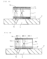
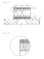
- FIG. 1A is a perspective view showing an exemplary structure pattern of a piezoelectric resonator according to a first embodiment of the present invention.
- FIG. 1B is a cross-sectional view taken along line C-C shown in FIG. 1A.
- the piezoelectric resonator according to the first embodiment is structured such that on a substrate 5 having a cavity 4 provided therein, a lower electrode 3, a piezoelectric body 1, a spurious component control layer 16, and an upper electrode 2 are formed in this order from bottom up.
- the upper electrode 2 and the lower electrode 3 are composed of, for example, molybdenum (Mo).
- the piezoelectric body 1 is composed of, for example, a piezoelectric material such as aluminum nitride (AlN).
- the spurious component control layer 16 is composed of a metallic material, a dielectric material, or a piezoelectric material (which is different from the material of the piezoelectric body 1 included in the piezoelectric resonator).
- the spurious component control layer 16 is composed of silicon dioxide (SiO 2 or silicon nitride (SiN). Note that depending on the material, the spurious component control layer 16 can be used as an etching stopper in a production process of the piezoelectric resonator, thereby simplifying the production process.
- the cavity 4 is provided in the form of, for example, a truncated pyramid vertically penetrating through the substrate 5.
- the piezoelectric resonator includes an additional layer, i.e., the spurious component control layer, which is composed of, for example, a metallic material, a dielectric material, or a piezoelectric material (which is different from the material of the piezoelectric body 1 included in the piezoelectric resonator)
- the spurious component control layer which is composed of, for example, a metallic material, a dielectric material, or a piezoelectric material (which is different from the material of the piezoelectric body 1 included in the piezoelectric resonator)
- variations in energy and frequency occur due to differences in elastic constant and density between the piezoelectric body and the additional layer.
- the spurious component control layer is formed in a position in the vicinity of the maximum distortion point in the portion A and the maximum vibration point in the portion B, the resonance frequency is increased in the portion A which is a source of generating spurious components, while being decreased in the portion B which is a source of generating main resonance.
- the frequency of the spurious components so as to be distanced from the resonance frequency of the main resonance.
- the spurious component control layer is formed in a position in the vicinity of the maximum vibration points both in the portion A and the portion B, there is a difference in variation of resonance frequencies due to a difference between distribution displacement distributions in the portions.
- spurious components are generated because the piezoelectric resonator is supported by the substrate 5.
- the spurious vibration is generated due to vibration of a supporting portion (for example, a fixed end 5a) while a portion with two free ends above the cavity 4 is longitudinally vibrating in the thickness direction at the resonance frequency f1.
- a supporting portion for example, a fixed end 5a
- the portion B in which the piezoelectric resonator is not supported
- the symbols Mn, Sn1, and Sn2 shown in FIG. 2A each indicate a portion as a node in the vibration displacement distribution.
- the node is a portion, which does not vibrate, and located at a maximum distortion point to which great distortion is applied.
- the piezoelectric resonator according to the first embodiment is structured such that the spurious component control layer 16 is formed between the upper and lower electrodes 2 and 3 (specifically, between the upper electrode 2 and the piezoelectric body 1), and therefore greatly influences excitation of vibration.
- the thickness of the portion B corresponds to a 1/2 wavelength of vibration at the resonance frequency f1
- the thickness of the portion A corresponds to a 3/4 wavelength of vibration at the resonance frequency f2.
- the resonance frequency f2 of the portion A is higher than the resonance frequency f1 of the portion B because the portion A has the fixed end 5a at an interface between the lower electrode 3 and the substrate 5 (FIG. 2A). Further, in comparison with the resonance frequency f1 of the portion B, the resonance frequency f2 of the portion A is more susceptible to influences of an elastic constant, a dielectric constant, and the presence or absence of a piezoelectric effect of the additionally provided spurious component control layer, because the portion A and the portion B differ from each other in the position of a vibration node.
- the vibration displacement distribution at the resonance frequency f2 varies greater than the vibration displacement distribution at the resonance frequency f1. Accordingly, in the case where the spurious component control layer 16 is additionally provided, the influence caused to the vibration of the portion B by a supporting portion (for example, the fixed end 5a) considerably varies as compared to a where no spurious component control layer 16 is additionally provided. Because of the above-described effects, a variation of the spurious frequency due to addition of the spurious component control layer 16 is greater than a variation of the resonance frequency of a main resonance due to addition of the spurious component control layer 16.
- the present invention achieves the above-described effects by additionally providing the spurious component control layer 16 with consideration of the vibration displacement distribution, such that spurious components, which are generated because the lower electrode 3 is supported by the substrate 5 in the portion A, occur at a frequency other than the resonance frequency fr and the antiresonance frequency fa.
- the resonance frequency f2 of the portion A corresponds to 3/4 wavelength vibration
- a resonance for achieving the effects of the present invention is not limited to 3/4 wavelength resonance (f2) as described above.
- a piezoelectric resonator having an admittance response, in which no spurious component occurs between the resonance frequency fr and the antiresonance frequency fa, can be realized by additionally providing the spurious component control layer 16 with consideration of the difference in displacement distribution between the portion B, in which the lower electrode 3 is out of contact with the substrate 5, and the portion A, in which the lower electrode 3 (at the bottom) with the substrate 5.
- the spurious component control layer 16 is formed between the piezoelectric body 1 and the upper electrode 2, it is possible to solve a conventional problemwhere adhesive strength between the piezoelectric body 1 and the upper electrode 2 is insufficient and unreliable. Thus, it is possible to increase the reliability of the piezoelectric resonator.
- the spurious component control layer to be additionallyprovidedtothepiezoelectricresonatorisnotlimited to the first embodiment in terms of the number, position, type, thickness, etc., which can be freely set depending on desired purposes and effects (as will be described in the second embodiment) .
- the first embodiment has been described with respect to a case where the spurious component control layer is formed such that the spurious frequency is equal to or more than the antiresonance frequency fa, the spurious component control layer may be formed such that the spurious frequency is less than the resonance frequency fr.
- a temperature coefficient of the resonance frequency of the piezoelectric body 1 is generally considerable. Accordingly, if the spurious component control layer 16 is composed, for example, SiO 2 , it is possible to compensate for a temperature characteristic of the elastic constant of the piezoelectric body 1, thereby reducing a variation of the resonance frequency of the piezoelectric resonator with respect to temperature. Asa result, it is possible to improve the temperature characteristic of the resonance frequency, thereby efficiently carrying out the temperature compensation.
- the thickness of the spurious component control layer 16 is t1 and the thickness of the piezoelectric body 1 is t2, it is preferred that the ratio t1/t2 between the thicknesses is less than or equal to 1/5. If the thickness of the spurious component control layer 16 is selected in this manner, it is possible to achieve an effect of controlling the spurious frequency without reducing the admittance frequency response.
- the spurious component control layer 16 is composed of a dielectric material having a mechanical quality factor higher than a mechanical quality factor of the material of the piezoelectric body 1.
- the Q-value of the resonator is increased, making it possible to obtain steeper skirt characteristics.
- the Q-value of the spurious component 13 to be generated can be high depending on properties of the spurious component control layer (FIG. 3A), even if the spurious components are shifted out of the range between the resonance frequency fr and the antiresonance frequency fa.
- a second embodiment is described with respect to another structure pattern of the piezoelectric resonator described in the first embodiment. Note that the structure pattern described in the second embodiment is merely an example, and various other structure patterns are conceivable.
- the piezoelectric resonator having a structure in which the spurious component control layer 16 is provided between the piezoelectric body 1 and the lower electrode 3, it is possible to control not only spurious components caused due to longitudinal vibration but also spurious components caused due to lateral vibration.
- FIG. 5A is a cross-sectional view showing an exemplary structure pattern of a piezoelectric resonator according to a third embodiment of the present invention.
- the piezoelectric resonator according to the third embodiment is structured such that on the substrate 5 having the cavity 4 provided therein, the lower electrode 3, the spurious component control layer 16, the piezoelectric body 1, the upper electrode 2, an additional piezoelectric body 51, and an additional electrode 52 are formed in this order from bottom up.
- the upper electrode 2, the lower electrode 3, and the additional electrode 52 are composed of, for example, molybdenum (Mo).
- the piezoelectric body 1 and the additional piezoelectric body 51 are composed of, for example, a piezoelectric material such as aluminum nitride (AlN).
- the spurious component control layer 16 is composed of a metallic material, adielectricmaterial, orapiezoelectricmaterial (which is different from the material of the piezoelectric body 1 included in the piezoelectric resonator).
- the spurious component control layer 16 is composed of silicon dioxide (SiO 2 ) or silicon nitride (SiN). Note that depending on the material, the spurious component control layer 16 can be used as an etching stopper in a production process of the piezoelectric resonator, thereby simplifying the production process.
- the cavity 4 is provided in the formof, for example, a truncated pyramid vertically penetrating through the substrate 5.
- the additional electrode 52, the additional piezoelectric body 51, and the upper electrode 2 form a first vibration portion 101.
- the upper electrode 2, the piezoelectric body 1, the spurious component control layer 16, and the lower electrode 3 form a second vibration portion 102.
- electrical energy applied between the additional electrode 52 and the upper electrode 2 is converted into mechanical energy by the first vibration portion 101, and then transmitted to the second vibration portion 102.
- the transmitted mechanical energy is converted back into electrical energy, and released from the upper electrode 2 and the lower electrode 3.
- by providing the spurious component control layer 16 as in the first embodiment it is made possible to cause variation of the spurious frequency to become greater than variation in resonance frequency of the main resonance of the piezoelectric resonator.
- FIGs. 5B-SE are views showing other exemplary structure patterns of the piezoelectric resonator according to the third embodiment.
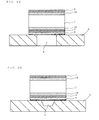
- FIG. 6A is a cross-sectional view showing an exemplary structure pattern of a piezoelectric resonator according to a fourth embodiment of the present invention.
- the piezoelectric resonator according to the fourth embodiment is structured such that on the substrate 5, an acoustic mirror 60, the lower electrode 3, the spurious component control layer 16, the piezoelectric body 1, and the upper electrode 2 are formed in this order from bottom up.
- the upper electrode 2 and the lower electrode 3 are composed of, for example, molybdenum (Mo).
- the piezoelectric body 1 is composed of, for example, a piezoelectric material such as aluminum nitride (AlN).
- the spurious component control layer 16 is composed of a metallic material, a dielectric material, or a piezoelectric material (which is different from the material of the piezoelectric body 1 included in the piezoelectric resonator).
- the spurious component control layer 16 is composed of silicon dioxide (SiO 2 or silicon nitride (SiN). Note that depending on the material, the spurious component control layer 16 can be used as an etching stopper in a production process of the piezoelectric resonator, thereby simplifying the production process.
- the acoustic mirror 60 plays a role similar to that of the cavity 4, and is operable to trap resonant vibration of a vibration portion 10 within the vibration portion 10.
- the acoustic mirror 60 is structured by laminating at least two types of layers each having an acoustic impedance different from that of the other layer.
- a low acoustic impedance layer 61 and a high acoustic impedance layer 62 alternate with each other.
- Each of the low acoustic impedance layer 61 and the high acoustic impedance layer 62 has a thickness equal to 1/4 of a corresponding wavelength.
- the low acoustic impedance layer 61 is situated below the lower electrode 3.
- FIGs. 6B-6D are views showing other exemplary structure patterns of the piezoelectric resonator according to the fourth embodiment.
- the spurious component control layer used in the fourth embodiment is composed of amaterial having a low acoustic impedance in directions other than the thickness direction as compared to acoustic impedances of the piezoelectric body 1, the upper electrode 2, and the lower electrode 3.
- a difference in acoustic impedance between the thickness direction and another direction e.g. , a radial direction
- a similar effect can be achieved by using a difference in acoustic impedance.
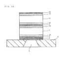
- FIG. 7A is a cross-sectional view showing an exemplary structure pattern of the piezoelectric resonator according to the fifth embodiment of the present invention.
- FIG. 7B is an enlarged view of a circled portion shown in FIG. 7A.
- the piezoelectric resonator according to the fifth embodiment is structured such that three spurious component control layers 6, 16, and 26 are different in thickness from each other. Due to differences in thickness, vibration displacement distribution varies as shown in FIG. 7B.
- the spurious component control layers 6, 16, and 26 are composed of a material having an elastic constant (Young's modulus) smaller than that of the piezoelectric body 1.
- the spurious component control layers 6, 16, and 26 can be composed of a metallic material, a dielectric material, or a piezoelectric material (which is different from the material of the piezoelectric body 1 included in the piezoelectric resonator).
- the spurious component control layers 6, 16, and 26 are composed of a material different in elastic constant and density (additionally, dielectric constant and/or piezoelectric effect) from a material of a vibration portion, it is possible to prevent, based on differences in elastic constant and density (additionally, dielectric constant and/or piezoelectric effect) between the materials, any spurious component due to influences by a fixed portion from occurring between the resonance frequency fr and the antiresonance frequency fa.
- the spurious component control layers 6, 16, and 26 may be different from each other in terms of material. In such a case, a greater effect can be achieved by selecting thicknesses and materials of the spurious component control layer 6, 16, and 26, such that the position of a vibration node in the portion A and the position of a vibration antinode in the portion B are closer to each other.
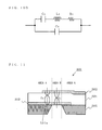
- FIG. 8A is a diagram showing an exemplary filter 7 including piezoelectric resonators of the present invention.
- the filter 7 shown in FIG. 8A is a single stage ladder filter in which the piezoelectric resonators are connected so as to form an L shape.
- a first piezoelectric resonator 71 is connected so as to operate as a series resonator. Specifically, the first piezoelectric resonator 71 is connected in series between an input terminal 73 and an output terminal 74.
- a second piezoelectric resonator 72 is connected so as to operate as a parallel resonator. Specifically, the second piezoelectric resonator 72 is connected between a ground plane and a path from the input terminal 73 to the output terminal 74.
- the first piezoelectric resonator 71 and the second piezoelectric resonator 72 are optimally controlled in terms of spurious frequency, and therefore it is possible to realize the filter 7 so as to have a satisfactory frequency response.
- the ladder filter may be a multiple stage filter as shown in FIG. 8B or may be a lattice-filter.
- FIG. 9 shows a duplexer 9 including the multi stage ladder filter shown in FIG. 8B.
- the duplexer 9 includes: a Tx filter (a transmission filter) 91 consisting of a plurality of piezoelectric resonators; an Rx filter (a reception filter) 92 consisting of a plurality of piezoelectric resonators; and a phase-shift circuit 93 consisting of two transmission lines.
- the Tx filter 91 and the Rx filter 92 include the piezoelectric resonators which are optimally controlled in terms of spurious frequency, and therefore it is possible to realize the duplexer 9 so as to have a satisfactory frequency response.
- the duplexer 9 is not limited by FIG. 9 in terms of the number of filters and the number of stages of the piezoelectric resonators included in the filters, and can be freely designed.
Abstract

Description

Claims (19)
- A piezoelectric resonator vibrating at a predetermined frequency, the resonator comprising:a piezoelectric body (1);an upper electrode (2) formed in a direction of a top surface of the piezoelectric body (1);a lower electrode (3) formed in a direction of a bottom surface of the piezoelectric body (1);a spurious component control layer (6, 16, or 26) formed in order to prevent a spurious component from occurring between a resonance frequency and an antiresonance frequency; anda substrate (5) on which the piezoelectric body (1), the upper electrode (2) , the lower electrode (3) , and the spurious component control layer (6, 16, or 26) are laminated.
- A piezoelectric resonator according to claim 1, wherein the spurious component control layer (6, 16, or 26) is provided between the upper electrode (2) and the piezoelectric body (1).
- A piezoelectric resonator according to claim 1, wherein the spurious component control layer (6, 16, or 26) is provided between the piezoelectric body (1) and the lower electrode (3).
- A piezoelectric resonator according to claim 1, wherein the spurious component control layer (6, 16, or 26) is provided on the top surface of the upper electrode (2).
- A piezoelectric resonator according to claim 1, wherein the spurious component control layer (6, 16, or 26) is provided between the lower electrode (3) and the substrate (5).
- A piezoelectric resonator according to claim 1, wherein the spurious component control layer (6, 16, or 26) is provided between the upper electrode (2) and the piezoelectric body (1) and between the piezoelectric body (1) and the lower electrode (3).
- A piezoelectric resonator according to claim 1, wherein the spurious component control layer (6, 16, or 26) is provided between the piezoelectric body (1) and the lower electrode (3) and between the lower electrode (3) and the substrate (5).
- A piezoelectric resonator according to claim 6, wherein the spurious component control layer (6, 16, or 26) provided between the upper electrode (2) and the piezoelectric body (1) is composed of a material different from a material of the spurious component control layer (6, 16, or 26) provided between the piezoelectric body (1) and the lower electrode (3).
- A piezoelectric resonator according to claim 7, wherein the spurious component control layer (6, 16, or 26) provided between the piezoelectric body (1) and the lower electrode (3) is composed of a material different from a material of the spurious component control layer (6, 16, or 26) provided between the lower electrode (3) and the substrate (5).
- A piezoelectric resonator according to claim 1, further comprising:a second piezoelectric body (51) formed on a top surface of the upper electrode (2); anda second upper electrode (52) formed on a top surface of the second piezoelectric body (51).
- A piezoelectric resonator according to claim 1, wherein a thickness of the spurious component control layer (6, 16, or 26) is set so as to be less than or equal to one-fifth of a thickness of the piezoelectric body (1).
- A piezoelectric resonator according to claim 1, wherein the spurious component control layer (6, 16, or 26) is composed of a metallic material.
- A piezoelectric resonator according to claim 1, wherein the spurious component control layer (6, 16, or 26) is composed of a dielectric material.
- A piezoelectric resonator according to claim 1, wherein the spurious component control layer (6, 16, or 26) is composed of a piezoelectric material different from the material of the piezoelectric body (1).
- A piezoelectric resonator according to claim 1, wherein the substrate (5) has a cavity in a portion covered by the lower electrode (3), the cavity being formed without penetrating the substrate (5).
- A piezoelectric resonator according to claim 1, wherein the substrate (5) has a cavity in a portion covered by the lower electrode (3), the cavity being formed so as to penetrate the substrate (5).
- A piezoelectric resonator according to claim 1, wherein an acoustic mirror (60) is provided between the lower electrode (3) and the substrate (5), the acoustic mirror (60) being structured by alternately laminating a high acoustic impedance layer and a low acoustic impedance layer.
- A filter (7) having two or more piezoelectric resonators of claim 1 connected in a ladder form.
- A duplexer (9) comprising:a transmission filter (91) having two or more piezoelectric resonators of claim 1 connected in a ladder form;a reception filter (92) having two or more piezoelectric resonators of claim 1 connected in a ladder form; anda phase-shift circuit (93) for connecting the transmission filter (91) and the reception filter (92).
Applications Claiming Priority (2)
| Application Number | Priority Date | Filing Date | Title |
|---|---|---|---|
| JP2003324399 | 2003-09-17 | ||
| JP2003324399 | 2003-09-17 |
Publications (3)
| Publication Number | Publication Date |
|---|---|
| EP1517444A2 true EP1517444A2 (en) | 2005-03-23 |
| EP1517444A3 EP1517444A3 (en) | 2005-08-31 |
| EP1517444B1 EP1517444B1 (en) | 2009-11-04 |
Family
ID=34191299
Family Applications (1)
| Application Number | Title | Priority Date | Filing Date |
|---|---|---|---|
| EP04021697A Expired - Fee Related EP1517444B1 (en) | 2003-09-17 | 2004-09-13 | Piezoelectric resonator, filter, and duplexer |
Country Status (5)
| Country | Link |
|---|---|
| US (2) | US7259498B2 (en) |
| EP (1) | EP1517444B1 (en) |
| JP (1) | JP2005117641A (en) |
| CN (1) | CN1599244B (en) |
| DE (1) | DE602004023908D1 (en) |
Cited By (5)
| Publication number | Priority date | Publication date | Assignee | Title |
|---|---|---|---|---|
| GB2432980A (en) * | 2005-11-30 | 2007-06-06 | Agilent Technologies Inc | Film bulk acoustic resonator (FBAR) devices with temperature compensation layers |
| US7242270B2 (en) | 2003-10-30 | 2007-07-10 | Avago Technologies Wireless Ip (Singapore) Pte. Ltd. | Decoupled stacked bulk acoustic resonator-based band-pass filter |
| GB2423428B (en) * | 2003-10-30 | 2007-09-05 | Agilent Technologies Inc | Temperature-compensated film bulk acoustic resonator (fbar) devices |
| US7915786B2 (en) | 2007-08-14 | 2011-03-29 | Taiyo Yuden Co., Ltd. | Elastic boundary wave device |
| US9859205B2 (en) | 2011-01-31 | 2018-01-02 | Avago Technologies General Ip (Singapore) Pte. Ltd. | Semiconductor device having an airbridge and method of fabricating the same |
Families Citing this family (98)
| Publication number | Priority date | Publication date | Assignee | Title |
|---|---|---|---|---|
| US7275292B2 (en) | 2003-03-07 | 2007-10-02 | Avago Technologies Wireless Ip (Singapore) Pte. Ltd. | Method for fabricating an acoustical resonator on a substrate |
| EP1528677B1 (en) * | 2003-10-30 | 2006-05-10 | Agilent Technologies, Inc. | Film acoustically-coupled transformer with two reverse c-axis piezoelectric elements |
| US6946928B2 (en) * | 2003-10-30 | 2005-09-20 | Agilent Technologies, Inc. | Thin-film acoustically-coupled transformer |
| US7019605B2 (en) * | 2003-10-30 | 2006-03-28 | Larson Iii John D | Stacked bulk acoustic resonator band-pass filter with controllable pass bandwidth |
| US7400217B2 (en) * | 2003-10-30 | 2008-07-15 | Avago Technologies Wireless Ip Pte Ltd | Decoupled stacked bulk acoustic resonator band-pass filter with controllable pass bandwith |
| DE102004035812A1 (en) * | 2004-07-23 | 2006-03-16 | Epcos Ag | Resonant bulk acoustic wave resonator |
| US7388454B2 (en) | 2004-10-01 | 2008-06-17 | Avago Technologies Wireless Ip Pte Ltd | Acoustic resonator performance enhancement using alternating frame structure |
| US8981876B2 (en) | 2004-11-15 | 2015-03-17 | Avago Technologies General Ip (Singapore) Pte. Ltd. | Piezoelectric resonator structures and electrical filters having frame elements |
| US7202560B2 (en) | 2004-12-15 | 2007-04-10 | Avago Technologies Wireless Ip (Singapore) Pte. Ltd. | Wafer bonding of micro-electro mechanical systems to active circuitry |
| US7791434B2 (en) | 2004-12-22 | 2010-09-07 | Avago Technologies Wireless Ip (Singapore) Pte. Ltd. | Acoustic resonator performance enhancement using selective metal etch and having a trench in the piezoelectric |
| DE102004062312B3 (en) * | 2004-12-23 | 2006-06-01 | Infineon Technologies Ag | Piezoelectric resonator, e.g. in mobile telephones, has a piezoelectric layer with a first resonance frequency temperature coefficient with a first polarity sign and electrodes |
| US7427819B2 (en) * | 2005-03-04 | 2008-09-23 | Avago Wireless Ip Pte Ltd | Film-bulk acoustic wave resonator with motion plate and method |
| US7369013B2 (en) * | 2005-04-06 | 2008-05-06 | Avago Technologies Wireless Ip Pte Ltd | Acoustic resonator performance enhancement using filled recessed region |
| US7436269B2 (en) * | 2005-04-18 | 2008-10-14 | Avago Technologies Wireless Ip (Singapore) Pte. Ltd. | Acoustically coupled resonators and method of making the same |
| US7934884B2 (en) * | 2005-04-27 | 2011-05-03 | Lockhart Industries, Inc. | Ring binder cover |
| US7443269B2 (en) | 2005-07-27 | 2008-10-28 | Avago Technologies General Ip (Singapore) Pte. Ltd. | Method and apparatus for selectively blocking radio frequency (RF) signals in a radio frequency (RF) switching circuit |
| US7868522B2 (en) * | 2005-09-09 | 2011-01-11 | Avago Technologies Wireless Ip (Singapore) Pte. Ltd. | Adjusted frequency temperature coefficient resonator |
| US7391286B2 (en) * | 2005-10-06 | 2008-06-24 | Avago Wireless Ip Pte Ltd | Impedance matching and parasitic capacitor resonance of FBAR resonators and coupled filters |
| US7423503B2 (en) * | 2005-10-18 | 2008-09-09 | Avago Technologies Wireless Ip (Singapore) Pte. Ltd. | Acoustic galvanic isolator incorporating film acoustically-coupled transformer |
| US7675390B2 (en) | 2005-10-18 | 2010-03-09 | Avago Technologies Wireless Ip (Singapore) Pte. Ltd. | Acoustic galvanic isolator incorporating single decoupled stacked bulk acoustic resonator |
| US7525398B2 (en) * | 2005-10-18 | 2009-04-28 | Avago Technologies General Ip (Singapore) Pte. Ltd. | Acoustically communicating data signals across an electrical isolation barrier |
| US7737807B2 (en) | 2005-10-18 | 2010-06-15 | Avago Technologies Wireless Ip (Singapore) Pte. Ltd. | Acoustic galvanic isolator incorporating series-connected decoupled stacked bulk acoustic resonators |
| US7463499B2 (en) * | 2005-10-31 | 2008-12-09 | Avago Technologies General Ip (Singapore) Pte Ltd. | AC-DC power converter |
| EP2214433B1 (en) * | 2006-01-11 | 2012-11-21 | Qualcomm Incorporated | Communications method and apparatus for transmitting priority information via beacon signals |
| US7612636B2 (en) * | 2006-01-30 | 2009-11-03 | Avago Technologies Wireless Ip (Singapore) Pte. Ltd. | Impedance transforming bulk acoustic wave baluns |
| KR101302132B1 (en) * | 2006-02-06 | 2013-09-03 | 삼성전자주식회사 | Filter module providing function related to multi band and method thereof |
| US7746677B2 (en) | 2006-03-09 | 2010-06-29 | Avago Technologies Wireless Ip (Singapore) Pte. Ltd. | AC-DC converter circuit and power supply |
| US20070210724A1 (en) * | 2006-03-09 | 2007-09-13 | Mark Unkrich | Power adapter and DC-DC converter having acoustic transformer |
| US20070210748A1 (en) * | 2006-03-09 | 2007-09-13 | Mark Unkrich | Power supply and electronic device having integrated power supply |
| US7479685B2 (en) | 2006-03-10 | 2009-01-20 | Avago Technologies General Ip (Singapore) Pte. Ltd. | Electronic device on substrate with cavity and mitigated parasitic leakage path |
| US7508286B2 (en) * | 2006-09-28 | 2009-03-24 | Avago Technologies Wireless Ip (Singapore) Pte. Ltd. | HBAR oscillator and method of manufacture |
| JP2008172711A (en) * | 2007-01-15 | 2008-07-24 | Hitachi Media Electoronics Co Ltd | Thin film bulk acoustic wave resonator, filter, and high frequency module using it |
| JP2008182511A (en) * | 2007-01-25 | 2008-08-07 | Seiko Epson Corp | Bulk acoustic vibrator, compensating method for frequency temperature characteristic thereof, and manufacturing method thereof |
| US20080202239A1 (en) * | 2007-02-28 | 2008-08-28 | Fazzio R Shane | Piezoelectric acceleration sensor |
| US7791435B2 (en) | 2007-09-28 | 2010-09-07 | Avago Technologies Wireless Ip (Singapore) Pte. Ltd. | Single stack coupled resonators having differential output |
| CN101960717B (en) * | 2008-03-04 | 2014-04-23 | 太阳诱电株式会社 | Film bulk acoustic resonator, filter, communication module and communication apparatus |
| US7855618B2 (en) | 2008-04-30 | 2010-12-21 | Avago Technologies Wireless Ip (Singapore) Pte. Ltd. | Bulk acoustic resonator electrical impedance transformers |
| US7732977B2 (en) | 2008-04-30 | 2010-06-08 | Avago Technologies Wireless Ip (Singapore) | Transceiver circuit for film bulk acoustic resonator (FBAR) transducers |
| US8902023B2 (en) | 2009-06-24 | 2014-12-02 | Avago Technologies General Ip (Singapore) Pte. Ltd. | Acoustic resonator structure having an electrode with a cantilevered portion |
| US8248185B2 (en) | 2009-06-24 | 2012-08-21 | Avago Technologies Wireless Ip (Singapore) Pte. Ltd. | Acoustic resonator structure comprising a bridge |
| JP2011041136A (en) * | 2009-08-17 | 2011-02-24 | Taiyo Yuden Co Ltd | Elastic wave device and method for manufacturing the same |
| FR2951024B1 (en) * | 2009-10-01 | 2012-03-23 | St Microelectronics Sa | METHOD FOR MANUFACTURING BAW RESONATOR WITH HIGH QUALITY FACTOR |
| FR2951023B1 (en) * | 2009-10-01 | 2012-03-09 | St Microelectronics Sa | METHOD FOR MANUFACTURING MONOLITHIC OSCILLATORS WITH BAW RESONATORS |
| FR2951026B1 (en) | 2009-10-01 | 2011-12-02 | St Microelectronics Sa | METHOD FOR MANUFACTURING BAW RESONATORS ON A SEMICONDUCTOR WAFER |
| US8193877B2 (en) | 2009-11-30 | 2012-06-05 | Avago Technologies Wireless Ip (Singapore) Pte. Ltd. | Duplexer with negative phase shifting circuit |
| US8796904B2 (en) | 2011-10-31 | 2014-08-05 | Avago Technologies General Ip (Singapore) Pte. Ltd. | Bulk acoustic resonator comprising piezoelectric layer and inverse piezoelectric layer |
| US9243316B2 (en) | 2010-01-22 | 2016-01-26 | Avago Technologies General Ip (Singapore) Pte. Ltd. | Method of fabricating piezoelectric material with selected c-axis orientation |
| US8253513B2 (en) * | 2010-03-16 | 2012-08-28 | Hao Zhang | Temperature compensated thin film acoustic wave resonator |
| US9197185B2 (en) | 2010-04-29 | 2015-11-24 | Avago Technologies General Ip (Singapore) Pte. Ltd. | Resonator device including electrodes with buried temperature compensating layers |
| US9479139B2 (en) * | 2010-04-29 | 2016-10-25 | Avago Technologies General Ip (Singapore) Pte. Ltd. | Resonator device including electrode with buried temperature compensating layer |
| CN101895272B (en) * | 2010-07-12 | 2013-01-30 | 陈新 | Method for inhibiting spurious response of quartz crystal resonator |
| US8830012B2 (en) * | 2010-09-07 | 2014-09-09 | Wei Pang | Composite bulk acoustic wave resonator |
| US9048812B2 (en) | 2011-02-28 | 2015-06-02 | Avago Technologies General Ip (Singapore) Pte. Ltd. | Bulk acoustic wave resonator comprising bridge formed within piezoelectric layer |
| US9154112B2 (en) | 2011-02-28 | 2015-10-06 | Avago Technologies General Ip (Singapore) Pte. Ltd. | Coupled resonator filter comprising a bridge |
| US9203374B2 (en) | 2011-02-28 | 2015-12-01 | Avago Technologies General Ip (Singapore) Pte. Ltd. | Film bulk acoustic resonator comprising a bridge |
| US9148117B2 (en) | 2011-02-28 | 2015-09-29 | Avago Technologies General Ip (Singapore) Pte. Ltd. | Coupled resonator filter comprising a bridge and frame elements |
| US9425764B2 (en) | 2012-10-25 | 2016-08-23 | Avago Technologies General Ip (Singapore) Pte. Ltd. | Accoustic resonator having composite electrodes with integrated lateral features |
| US9083302B2 (en) | 2011-02-28 | 2015-07-14 | Avago Technologies General Ip (Singapore) Pte. Ltd. | Stacked bulk acoustic resonator comprising a bridge and an acoustic reflector along a perimeter of the resonator |
| US9136818B2 (en) | 2011-02-28 | 2015-09-15 | Avago Technologies General Ip (Singapore) Pte. Ltd. | Stacked acoustic resonator comprising a bridge |
| US9401692B2 (en) | 2012-10-29 | 2016-07-26 | Avago Technologies General Ip (Singapore) Pte. Ltd. | Acoustic resonator having collar structure |
| US9444426B2 (en) | 2012-10-25 | 2016-09-13 | Avago Technologies General Ip (Singapore) Pte. Ltd. | Accoustic resonator having integrated lateral feature and temperature compensation feature |
| US9490771B2 (en) | 2012-10-29 | 2016-11-08 | Avago Technologies General Ip (Singapore) Pte. Ltd. | Acoustic resonator comprising collar and frame |
| US8575820B2 (en) | 2011-03-29 | 2013-11-05 | Avago Technologies General Ip (Singapore) Pte. Ltd. | Stacked bulk acoustic resonator |
| US9490418B2 (en) | 2011-03-29 | 2016-11-08 | Avago Technologies General Ip (Singapore) Pte. Ltd. | Acoustic resonator comprising collar and acoustic reflector with temperature compensating layer |
| US9246473B2 (en) | 2011-03-29 | 2016-01-26 | Avago Technologies General Ip (Singapore) Pte. Ltd. | Acoustic resonator comprising collar, frame and perimeter distributed bragg reflector |
| FR2973970B1 (en) * | 2011-04-07 | 2013-04-12 | Commissariat Energie Atomique | DEVICE USING A FILTER BASED ON RESONATORS |
| US9154111B2 (en) | 2011-05-20 | 2015-10-06 | Avago Technologies General Ip (Singapore) Pte. Ltd. | Double bulk acoustic resonator comprising aluminum scandium nitride |
| US9917567B2 (en) | 2011-05-20 | 2018-03-13 | Avago Technologies General Ip (Singapore) Pte. Ltd. | Bulk acoustic resonator comprising aluminum scandium nitride |
| US20120293278A1 (en) * | 2011-05-20 | 2012-11-22 | Avago Technologies Wireless Ip (Singapore) Pte. Ltd. | Stacked bulk acoustic resonator comprising distributed bragg reflector |
| US8350445B1 (en) | 2011-06-16 | 2013-01-08 | Avago Technologies Wireless Ip (Singapore) Pte. Ltd. | Bulk acoustic resonator comprising non-piezoelectric layer and bridge |
| US8922302B2 (en) | 2011-08-24 | 2014-12-30 | Avago Technologies General Ip (Singapore) Pte. Ltd. | Acoustic resonator formed on a pedestal |
| US9525399B2 (en) * | 2011-10-31 | 2016-12-20 | Avago Technologies General Ip (Singapore) Pte. Ltd. | Planarized electrode for improved performance in bulk acoustic resonators |
| CN102904546B (en) * | 2012-08-30 | 2016-04-13 | 中兴通讯股份有限公司 | The adjustable piezoelectric acoustic wave resonator of a kind of temperature compensation capability |
| US9385684B2 (en) | 2012-10-23 | 2016-07-05 | Avago Technologies General Ip (Singapore) Pte. Ltd. | Acoustic resonator having guard ring |
| DE102012111121A1 (en) * | 2012-11-19 | 2014-05-22 | Epcos Ag | Electroacoustic component and method of manufacture |
| WO2014094884A1 (en) * | 2012-12-21 | 2014-06-26 | Epcos Ag | Baw component, lamination for a baw component, and method for manufacturing a baw component, said baw component comprising two stacked piezoelectric materials that differ |
| KR101959204B1 (en) * | 2013-01-09 | 2019-07-04 | 삼성전자주식회사 | Radio frequency filter and manufacturing mathod thereof |
| JP6336712B2 (en) * | 2013-01-28 | 2018-06-06 | 太陽誘電株式会社 | Piezoelectric thin film resonator, filter and duplexer |
| US9608192B2 (en) | 2013-03-28 | 2017-03-28 | Avago Technologies General Ip (Singapore) Pte. Ltd. | Temperature compensated acoustic resonator device |
| US9450167B2 (en) | 2013-03-28 | 2016-09-20 | Avago Technologies General Ip (Singapore) Pte. Ltd. | Temperature compensated acoustic resonator device having an interlayer |
| JP6400970B2 (en) * | 2014-07-25 | 2018-10-03 | 太陽誘電株式会社 | Filters and duplexers |
| US9621126B2 (en) * | 2014-10-22 | 2017-04-11 | Avago Technologies General Ip (Singapore) Pte. Ltd. | Bulk acoustic resonator device including temperature compensation structure comprising low acoustic impedance layer |
| US9698756B2 (en) | 2014-12-24 | 2017-07-04 | Qorvo Us, Inc. | Acoustic RF resonator parallel capacitance compensation |
| WO2017051572A1 (en) * | 2015-09-21 | 2017-03-30 | 株式会社村田製作所 | Resonator and resonance device |
| US10581403B2 (en) | 2016-07-11 | 2020-03-03 | Qorvo Us, Inc. | Device having a titanium-alloyed surface |
| US11050412B2 (en) | 2016-09-09 | 2021-06-29 | Qorvo Us, Inc. | Acoustic filter using acoustic coupling |
| US11165412B2 (en) | 2017-01-30 | 2021-11-02 | Qorvo Us, Inc. | Zero-output coupled resonator filter and related radio frequency filter circuit |
| US11165413B2 (en) | 2017-01-30 | 2021-11-02 | Qorvo Us, Inc. | Coupled resonator structure |
| US11336255B2 (en) | 2017-02-16 | 2022-05-17 | Acoustic Wave Device Labo., Ltd. | Acoustic wave element and method for manufacturing same |
| US11152913B2 (en) | 2018-03-28 | 2021-10-19 | Qorvo Us, Inc. | Bulk acoustic wave (BAW) resonator |
| US11146247B2 (en) * | 2019-07-25 | 2021-10-12 | Qorvo Us, Inc. | Stacked crystal filter structures |
| CN111010120A (en) * | 2019-09-20 | 2020-04-14 | 天津大学 | Bulk acoustic wave resonator, filter, and electronic device having adjustment layer |
| US11757430B2 (en) | 2020-01-07 | 2023-09-12 | Qorvo Us, Inc. | Acoustic filter circuit for noise suppression outside resonance frequency |
| US11146245B2 (en) | 2020-01-13 | 2021-10-12 | Qorvo Us, Inc. | Mode suppression in acoustic resonators |
| US11146246B2 (en) | 2020-01-13 | 2021-10-12 | Qorvo Us, Inc. | Phase shift structures for acoustic resonators |
| US11632097B2 (en) | 2020-11-04 | 2023-04-18 | Qorvo Us, Inc. | Coupled resonator filter device |
| US11575363B2 (en) | 2021-01-19 | 2023-02-07 | Qorvo Us, Inc. | Hybrid bulk acoustic wave filter |
| CN113810013B (en) * | 2021-09-23 | 2023-02-28 | 武汉敏声新技术有限公司 | Resonator, filter and duplexer |
Citations (2)
| Publication number | Priority date | Publication date | Assignee | Title |
|---|---|---|---|---|
| JPS59200518A (en) * | 1983-04-27 | 1984-11-13 | Murata Mfg Co Ltd | Thickness-shear vibrational parts |
| JPH0251908A (en) * | 1988-08-15 | 1990-02-21 | Murata Mfg Co Ltd | Piezoelectric resonator |
Family Cites Families (13)
| Publication number | Priority date | Publication date | Assignee | Title |
|---|---|---|---|---|
| JPS58137317A (en) * | 1982-02-09 | 1983-08-15 | Nec Corp | Thin-film piezoelectric compound oscillator |
| JPS6068711A (en) | 1983-09-26 | 1985-04-19 | Toshiba Corp | Piezoelectric thin film resonator |
| JPS60142607A (en) | 1983-12-29 | 1985-07-27 | Nec Corp | Piezoelectric thin film composite oscillator |
| JPS6382116A (en) | 1986-09-26 | 1988-04-12 | Matsushita Electric Ind Co Ltd | Piezoelectric thin film resonator and its manufacture |
| JPS63190413A (en) | 1987-02-02 | 1988-08-08 | Murata Mfg Co Ltd | Piezoelectric resonator |
| US5821833A (en) * | 1995-12-26 | 1998-10-13 | Tfr Technologies, Inc. | Stacked crystal filter device and method of making |
| US5872493A (en) | 1997-03-13 | 1999-02-16 | Nokia Mobile Phones, Ltd. | Bulk acoustic wave (BAW) filter having a top portion that includes a protective acoustic mirror |
| US6472954B1 (en) * | 2001-04-23 | 2002-10-29 | Agilent Technologies, Inc. | Controlled effective coupling coefficients for film bulk acoustic resonators |
| US6476536B1 (en) * | 2001-04-27 | 2002-11-05 | Nokia Corporation | Method of tuning BAW resonators |
| JP3879643B2 (en) * | 2002-09-25 | 2007-02-14 | 株式会社村田製作所 | Piezoelectric resonator, piezoelectric filter, communication device |
| JP2004304704A (en) * | 2003-04-01 | 2004-10-28 | Matsushita Electric Ind Co Ltd | Thin film acoustic resonator and thin film acoustic resonator circuit |
| JP2005094735A (en) * | 2003-08-12 | 2005-04-07 | Murata Mfg Co Ltd | Electronic component and method of manufacturing the same |
| JP2007202138A (en) * | 2005-12-28 | 2007-08-09 | Kyocera Corp | Thin film bulk acoustic resonator, filtering device with same and communication apparatus |
-
2004
- 2004-09-09 JP JP2004262767A patent/JP2005117641A/en active Pending
- 2004-09-13 DE DE602004023908T patent/DE602004023908D1/en active Active
- 2004-09-13 EP EP04021697A patent/EP1517444B1/en not_active Expired - Fee Related
- 2004-09-13 US US10/938,537 patent/US7259498B2/en not_active Ceased
- 2004-09-16 CN CN200410078757.9A patent/CN1599244B/en not_active Expired - Fee Related
-
2008
- 2008-02-08 US US12/068,675 patent/USRE42009E1/en not_active Expired - Fee Related
Patent Citations (2)
| Publication number | Priority date | Publication date | Assignee | Title |
|---|---|---|---|---|
| JPS59200518A (en) * | 1983-04-27 | 1984-11-13 | Murata Mfg Co Ltd | Thickness-shear vibrational parts |
| JPH0251908A (en) * | 1988-08-15 | 1990-02-21 | Murata Mfg Co Ltd | Piezoelectric resonator |
Non-Patent Citations (2)
| Title |
|---|
| PATENT ABSTRACTS OF JAPAN vol. 009, no. 061 (E-303), 19 March 1985 (1985-03-19) -& JP 59 200518 A (MURATA SEISAKUSHO:KK), 13 November 1984 (1984-11-13) * |
| PATENT ABSTRACTS OF JAPAN vol. 014, no. 216 (E-0924), 8 May 1990 (1990-05-08) -& JP 02 051908 A (MURATA MFG CO LTD), 21 February 1990 (1990-02-21) * |
Cited By (6)
| Publication number | Priority date | Publication date | Assignee | Title |
|---|---|---|---|---|
| US7242270B2 (en) | 2003-10-30 | 2007-07-10 | Avago Technologies Wireless Ip (Singapore) Pte. Ltd. | Decoupled stacked bulk acoustic resonator-based band-pass filter |
| GB2423428B (en) * | 2003-10-30 | 2007-09-05 | Agilent Technologies Inc | Temperature-compensated film bulk acoustic resonator (fbar) devices |
| GB2432980A (en) * | 2005-11-30 | 2007-06-06 | Agilent Technologies Inc | Film bulk acoustic resonator (FBAR) devices with temperature compensation layers |
| GB2432980B (en) * | 2005-11-30 | 2010-12-15 | Agilent Technologies Inc | Film bulk acoustic resonator (FBAR) devices with temperature compensation |
| US7915786B2 (en) | 2007-08-14 | 2011-03-29 | Taiyo Yuden Co., Ltd. | Elastic boundary wave device |
| US9859205B2 (en) | 2011-01-31 | 2018-01-02 | Avago Technologies General Ip (Singapore) Pte. Ltd. | Semiconductor device having an airbridge and method of fabricating the same |
Also Published As
| Publication number | Publication date |
|---|---|
| EP1517444A3 (en) | 2005-08-31 |
| EP1517444B1 (en) | 2009-11-04 |
| CN1599244A (en) | 2005-03-23 |
| US7259498B2 (en) | 2007-08-21 |
| JP2005117641A (en) | 2005-04-28 |
| USRE42009E1 (en) | 2010-12-28 |
| US20050057117A1 (en) | 2005-03-17 |
| DE602004023908D1 (en) | 2009-12-17 |
| CN1599244B (en) | 2010-05-26 |
Similar Documents
| Publication | Publication Date | Title |
|---|---|---|
| EP1517444A2 (en) | Piezoelectric resonator, filter, and duplexer | |
| US7893793B2 (en) | Film bulk acoustic wave resonator and method for manufacturing the same | |
| US7804383B2 (en) | Coupled lamb wave resonators filter | |
| US7236066B2 (en) | Film bulk acoustic resonator and filter circuit including a plurality of film bulk acoustic resonators | |
| US7005946B2 (en) | MEMS piezoelectric longitudinal mode resonator | |
| US7719388B2 (en) | Resonator operating with bulk acoustic waves | |
| US20060284703A1 (en) | Coupled FBAR filter | |
| US20070296513A1 (en) | Oscillator | |
| US7446455B2 (en) | Thin film elastic wave resonator | |
| CN1739237B (en) | Resonator filter structure having equal resonance frequencies | |
| GB2415307A (en) | FBAR acoustic resonator with reduced lateral or parasitic modes | |
| JP2005223479A (en) | Thin film bulk resonator, thin film bulk resonator filter, and manufacturing method of thin film bulk resonator | |
| US7477115B2 (en) | Piezoelectric resonator, method of manufacturing piezoelectric resonator, and filter, duplexer, and communication device using piezoelectric resonator | |
| JP2006513662A5 (en) | ||
| KR20010073196A (en) | Thin film piezoelectric element, method for manufacturing the same, and circuit element | |
| CN111884617A (en) | Resonator and preparation method thereof | |
| US7242130B2 (en) | Piezoelectric device, antenna duplexer, and method of manufacturing piezoelectric resonators used therefor | |
| US7531943B2 (en) | Acoustic resonator and filter | |
| US7230367B2 (en) | Piezoelectric resonator, production method thereof, filter, duplexer, and communication device | |
| US20090121809A1 (en) | Thin Film Elastic Wave Resonator | |
| JP2005260484A (en) | Piezoelectric resonator and electronic component equipped with the same | |
| JP2005160056A (en) | Piezoelectric device, antenna duplexer and method of manufacturing piezoelectric resonators used therefor | |
| JP2005210681A (en) | Piezoelectric resonator, production method therefor, filter using the resonator, duplexer, and communications device | |
| JP2005160057A (en) | Piezoelectric resonator, manufacturing method thereof, filter using the same, duplexer and communication apparatus | |
| KR100359967B1 (en) | Manufacturing method and circuit device of thin film piezoelectric element and thin film piezoelectric element |
Legal Events
| Date | Code | Title | Description |
|---|---|---|---|
| PUAI | Public reference made under article 153(3) epc to a published international application that has entered the european phase |
Free format text: ORIGINAL CODE: 0009012 |
|
| AK | Designated contracting states |
Kind code of ref document: A2 Designated state(s): AT BE BG CH CY CZ DE DK EE ES FI FR GB GR HU IE IT LI LU MC NL PL PT RO SE SI SK TR |
|
| AX | Request for extension of the european patent |
Extension state: AL HR LT LV MK |
|
| PUAL | Search report despatched |
Free format text: ORIGINAL CODE: 0009013 |
|
| AK | Designated contracting states |
Kind code of ref document: A3 Designated state(s): AT BE BG CH CY CZ DE DK EE ES FI FR GB GR HU IE IT LI LU MC NL PL PT RO SE SI SK TR |
|
| AX | Request for extension of the european patent |
Extension state: AL HR LT LV MK |
|
| 17P | Request for examination filed |
Effective date: 20050928 |
|
| AKX | Designation fees paid |
Designated state(s): DE FR GB |
|
| 17Q | First examination report despatched |
Effective date: 20070813 |
|
| RAP1 | Party data changed (applicant data changed or rights of an application transferred) |
Owner name: PANASONIC CORPORATION |
|
| GRAP | Despatch of communication of intention to grant a patent |
Free format text: ORIGINAL CODE: EPIDOSNIGR1 |
|
| GRAS | Grant fee paid |
Free format text: ORIGINAL CODE: EPIDOSNIGR3 |
|
| GRAA | (expected) grant |
Free format text: ORIGINAL CODE: 0009210 |
|
| AK | Designated contracting states |
Kind code of ref document: B1 Designated state(s): DE FR GB |
|
| REG | Reference to a national code |
Ref country code: GB Ref legal event code: FG4D |
|
| REF | Corresponds to: |
Ref document number: 602004023908 Country of ref document: DE Date of ref document: 20091217 Kind code of ref document: P |
|
| PLBE | No opposition filed within time limit |
Free format text: ORIGINAL CODE: 0009261 |
|
| STAA | Information on the status of an ep patent application or granted ep patent |
Free format text: STATUS: NO OPPOSITION FILED WITHIN TIME LIMIT |
|
| 26N | No opposition filed |
Effective date: 20100805 |
|
| PGFP | Annual fee paid to national office [announced via postgrant information from national office to epo] |
Ref country code: DE Payment date: 20130911 Year of fee payment: 10 |
|
| PGFP | Annual fee paid to national office [announced via postgrant information from national office to epo] |
Ref country code: FR Payment date: 20130910 Year of fee payment: 10 Ref country code: GB Payment date: 20130911 Year of fee payment: 10 |
|
| REG | Reference to a national code |
Ref country code: DE Ref legal event code: R119 Ref document number: 602004023908 Country of ref document: DE |
|
| GBPC | Gb: european patent ceased through non-payment of renewal fee |
Effective date: 20140913 |
|
| REG | Reference to a national code |
Ref country code: DE Ref legal event code: R119 Ref document number: 602004023908 Country of ref document: DE Effective date: 20150401 |
|
| REG | Reference to a national code |
Ref country code: FR Ref legal event code: ST Effective date: 20150529 |
|
| PG25 | Lapsed in a contracting state [announced via postgrant information from national office to epo] |
Ref country code: GB Free format text: LAPSE BECAUSE OF NON-PAYMENT OF DUE FEES Effective date: 20140913 Ref country code: DE Free format text: LAPSE BECAUSE OF NON-PAYMENT OF DUE FEES Effective date: 20150401 |
|
| PG25 | Lapsed in a contracting state [announced via postgrant information from national office to epo] |
Ref country code: FR Free format text: LAPSE BECAUSE OF NON-PAYMENT OF DUE FEES Effective date: 20140930 |