EP1517334A1 - On-chip diagnosis method and on-chip diagnosis block for memory repair with mixed redundancy (IO redundancy and word-register redundancy) - Google Patents
On-chip diagnosis method and on-chip diagnosis block for memory repair with mixed redundancy (IO redundancy and word-register redundancy) Download PDFInfo
- Publication number
- EP1517334A1 EP1517334A1 EP03292283A EP03292283A EP1517334A1 EP 1517334 A1 EP1517334 A1 EP 1517334A1 EP 03292283 A EP03292283 A EP 03292283A EP 03292283 A EP03292283 A EP 03292283A EP 1517334 A1 EP1517334 A1 EP 1517334A1
- Authority
- EP
- European Patent Office
- Prior art keywords
- array
- redundancy
- fill
- chip
- redundant
- Prior art date
- Legal status (The legal status is an assumption and is not a legal conclusion. Google has not performed a legal analysis and makes no representation as to the accuracy of the status listed.)
- Granted
Links
- 238000003745 diagnosis Methods 0.000 title claims abstract description 36
- 230000015654 memory Effects 0.000 title claims abstract description 27
- 238000000034 method Methods 0.000 title claims abstract description 16
- 238000003491 array Methods 0.000 claims abstract description 19
- 238000012360 testing method Methods 0.000 claims abstract description 6
- 238000004458 analytical method Methods 0.000 claims abstract description 5
- 238000013507 mapping Methods 0.000 claims abstract description 3
- 230000007547 defect Effects 0.000 description 11
- 238000005516 engineering process Methods 0.000 description 3
- 101100417881 Arabidopsis thaliana RRA1 gene Proteins 0.000 description 1
- 101100417882 Arabidopsis thaliana RRA2 gene Proteins 0.000 description 1
- 101100417883 Arabidopsis thaliana RRA3 gene Proteins 0.000 description 1
- 101100240020 Saccharomyces cerevisiae (strain ATCC 204508 / S288c) KRE33 gene Proteins 0.000 description 1
- 238000013459 approach Methods 0.000 description 1
- 230000001419 dependent effect Effects 0.000 description 1
- 238000011156 evaluation Methods 0.000 description 1
- 238000004519 manufacturing process Methods 0.000 description 1
Images





Classifications
-
- G—PHYSICS
- G11—INFORMATION STORAGE
- G11C—STATIC STORES
- G11C29/00—Checking stores for correct operation ; Subsequent repair; Testing stores during standby or offline operation
- G11C29/70—Masking faults in memories by using spares or by reconfiguring
- G11C29/72—Masking faults in memories by using spares or by reconfiguring with optimized replacement algorithms
-
- G—PHYSICS
- G11—INFORMATION STORAGE
- G11C—STATIC STORES
- G11C29/00—Checking stores for correct operation ; Subsequent repair; Testing stores during standby or offline operation
- G11C29/02—Detection or location of defective auxiliary circuits, e.g. defective refresh counters
-
- G—PHYSICS
- G11—INFORMATION STORAGE
- G11C—STATIC STORES
- G11C29/00—Checking stores for correct operation ; Subsequent repair; Testing stores during standby or offline operation
- G11C29/02—Detection or location of defective auxiliary circuits, e.g. defective refresh counters
- G11C29/022—Detection or location of defective auxiliary circuits, e.g. defective refresh counters in I/O circuitry
-
- G—PHYSICS
- G11—INFORMATION STORAGE
- G11C—STATIC STORES
- G11C29/00—Checking stores for correct operation ; Subsequent repair; Testing stores during standby or offline operation
- G11C29/02—Detection or location of defective auxiliary circuits, e.g. defective refresh counters
- G11C29/025—Detection or location of defective auxiliary circuits, e.g. defective refresh counters in signal lines
-
- G—PHYSICS
- G11—INFORMATION STORAGE
- G11C—STATIC STORES
- G11C29/00—Checking stores for correct operation ; Subsequent repair; Testing stores during standby or offline operation
- G11C29/04—Detection or location of defective memory elements, e.g. cell constructio details, timing of test signals
- G11C29/08—Functional testing, e.g. testing during refresh, power-on self testing [POST] or distributed testing
- G11C29/12—Built-in arrangements for testing, e.g. built-in self testing [BIST] or interconnection details
- G11C29/44—Indication or identification of errors, e.g. for repair
- G11C29/4401—Indication or identification of errors, e.g. for repair for self repair
Definitions
- the invention relates to diagnosis and repair of defects at memories on chips.
- the invention relates to an on chip diagnosis method and to an on chip diagnosis block.
- this object is achieved by an on chip diagnosis method according to claim 1 and by an on chip diagnosis block according to claim 3.
- a preferred and advantageous embodiment of the method according to the invention is subject matter of claim 2.
- Preferred and advantageous embodiments of the on chip diagnosis block according to the invention are subject matter od claims 4 to 6.
- the idea realised in the present invention allows to improve the yield with a mix of two types of redundancy: external (word-register) and internal redundancy (redundant IO only).
- the memories are tested in two steps:
- the size of the two arrays used is mainly dependent on the size of the redundancy (number of internal redundant IO and external word-register).
- the core of the present invention is the way to store (on chip) the defects during the BIST in these two arrays and the way to do (on chip) the diagnosis with these two arrays.
- the present invention allows to do easily a fast diagnosis in order to propose the best repair solution even if there are several types of defects (single, IO, cluster).
- FIG. 1 An embodiment of the invention will now be described with respect to an SRAM 4kx32 with 1 redundant IO and 3 redundant registers.
- SRAM embodying an on chip diagnosis block according to the invention is shown in Fig. 1.
- the word-register redundancy is carried out as external redundancy, and internal redundancy is the redundant IO only.
- the available redundancy of the embodiment shown in Fig. 1 consists of one complete redundant IO (IOR) inside the memory, and three redundant register addresses.
- Fig. 2 shows an example of a failure in the SRAM of Fig. 1, which failure is repairable with the available redundancy.
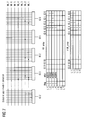
- the on chip diagnosis block according to the invention comprises two mandatory arrays ("fill_array” and "shift_array”). Examples for both arrays are shown in Fig. 3.
- the Figs. 4 to 13 show in a detailed view how to fill the two mandatory arrays (fill_array, shift_array) for diagnosis according to one embodiment of an on chip diagnosis method according to the invention. It has to mentioned once again that according to the invention the defects are stored on chip during BIST and the diagnosis is carried out on chip, too, using said two arrays (fill_array, shift_array).
- the reference element indicates for each line of the fill_array if there is one or more than one fault for each address stored.
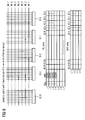
- the second element (called “difference element”) computes for each IO the difference between the reference element and the "fill_array(IO xx)" (cf. Fig. 15).
- Fig. 17 shows a flow chart of the test repair sequence.
Landscapes
- For Increasing The Reliability Of Semiconductor Memories (AREA)
- Tests Of Electronic Circuits (AREA)
- Techniques For Improving Reliability Of Storages (AREA)
Abstract
Description
- The invention relates to diagnosis and repair of defects at memories on chips. In particular the invention relates to an on chip diagnosis method and to an on chip diagnosis block.
- Memories are much denser than any logic. Since many bits need to be packed as tightly as possible, defects are part of any fabrication process. In order to avoid these defects and increase the yield, most memories have redundancy: internal redundancy (IO or WordLine) or external redundancy (word-register). Since most fails on memories are single cell fails, non-single cell types defects (IO) or cluster of fails. If one wishes to increase the yield to the maximum, then one has to mix all the redundancies available (internal and external).
- Several solutions to fix defects inside memories are used according to the state of the art:
- External redundancy only (HDFR from Infineon Technologies): This type of redundancy uses registers to replace failing words. It is well suited for single bit or small cluster fails. However, it is not suitable for BL or IO oriented failures.
- Internal redundancy (WordLine + IO) (MIR-TDR from Infineon Technologies): The main disadvantage is that this solution increases the access & cycle time in the memory block because one has to compare the actual address with the information stored in the fuse boxes. This type of redundancy is well suited for cluster of fails and non-single cell types defects (IO or WordLine defects).
- Words + WordLine + BL redundancy (as described in the European
patent application EP 03002698.3 "Memory Built-In Self
Repair (MBISR) circuits / devices and method for repairing
a memory comprising a Memory Built-In Self Repair (MBISR)
structure"; applicant: Infineon Technologies): The main
disadvantages of this approach are as follows:
- more than one BIST (Built-In Self Test) runs are needed (at least three),
- the usage of redundant wordline implies a lost in performances,
- the repair solution is hard-coded (first IO/BL, the WordLine, and finally Words),
- in some cases memories that could be repaired will be discarded, and
- a first evaluation of the additional logic needed seems that it will be expensive, in particular because a lot of comparisons are performed.
- It is an object of the present invention to provide an on chip diagnosis block for memory repair and an on chip diagnosis method for memory repair, which on chip diagnosis block and which on chip diagnosis method are able to overcome and least part of the disadvantages from the state of the art.
- According to the invention this object is achieved by an on chip diagnosis method according to
claim 1 and by an on chip diagnosis block according toclaim 3. - A preferred and advantageous embodiment of the method according to the invention is subject matter of
claim 2. Preferred and advantageous embodiments of the on chip diagnosis block according to the invention are subject matter odclaims 4 to 6. - The idea realised in the present invention allows to improve the yield with a mix of two types of redundancy: external (word-register) and internal redundancy (redundant IO only).
- The memories are tested in two steps:
- first one stores (during the BIST run) inside two arrays (one to keep the minimum error mapping and the other one to control the fill of the first one) the main information necessary for the final diagnose (to apply all redundancy resources needed), and
- then one performs the final diagnosis (based upon the analysis of said two arrays).
- The size of the two arrays used is mainly dependent on the size of the redundancy (number of internal redundant IO and external word-register).
- The core of the present invention is the way to store (on chip) the defects during the BIST in these two arrays and the way to do (on chip) the diagnosis with these two arrays.
- The invention provides the following advantages:
- It finds a good compromise to repair several types of defects and hence to increase yield.
- Diagnosis is done "On Chip", i.e. there is no need to do an external analysis. Therefore less time is needed for testing the chip.
- Diagnostic of the best repair solution is very fast.
- The number of additional gates needed to analyse errors is very small compared to method known from the state of the art.
- There is no impact on timings compared to a memory with internal redundant IO and WordLine.
- Only one BIST run is needed.
- Both IO and word-registers repair solutions are evaluated at the time.
- All fixable memories will be repaired, i.e. there is no possibility that fixable memories will be discarded.
- Independency from the architecture of the memory.
- Independency from the BIST algorithm.
- Independency from the kind of memory: SRAM, DRAM, CAM.
- Once all failures are detected in a memory, the present invention allows to do easily a fast diagnosis in order to propose the best repair solution even if there are several types of defects (single, IO, cluster).
- Examples of preferred and advantageous embodiments of the invention will now be described herein below with reference to the accompanying drawings in which
- Fig. 1
- is a schematic view of an embodiment of the invention with respect to an SRAM 4kx32,
- Fig. 2
- shows an example of a failure with respect to the SRAM of Fig. 1,
- Fig. 3
- shows an example of a fill_array and of a shift_array, respectively,
- Figs. 4 to 13
- show in a detailed view how, according to one embodiment of the method according to the invention, to fill the arrays of Fig. 3 during diagnosis of the failure shown in Fig. 2,
- Fig. 14
- shows how a reference element is built from the fill_array at the end of a BIST run,
- Fig. 15
- shows how difference elements are built from the reference element and the fill_array,
- Fig. 16
- shows how the redundant IO is fixed using the difference elements shown in Fig. 15, and
- Fig. 17
- is a flow chart of a test repair sequence.
- An embodiment of the invention will now be described with respect to an SRAM 4kx32 with 1 redundant IO and 3 redundant registers. Such an SRAM embodying an on chip diagnosis block according to the invention is shown in Fig. 1. As can be seen, the word-register redundancy is carried out as external redundancy, and internal redundancy is the redundant IO only. Summarizing, the available redundancy of the embodiment shown in Fig. 1 consists of one complete redundant IO (IOR) inside the memory, and three redundant register addresses.
- Fig. 2 shows an example of a failure in the SRAM of Fig. 1, which failure is repairable with the available redundancy.
- During a BIST run all these errors are produced. It has to be noted that some errors are produced several times, depending on the state of the BIST. Single error or multiple errors on the same word are possible.
- The on chip diagnosis block according to the invention comprises two mandatory arrays ("fill_array" and "shift_array"). Examples for both arrays are shown in Fig. 3.
- The size of the fill_array is defined by the total size of available redundancy. At the present example there are 1 redundant IO and 3 redundant word registers. The number of lines is defined by:
- The size of the shift_array depends on the number of redundant registers:
- With respect to the SRAM of Fig. 1 comprising the failure shown in Fig. 2 the Figs. 4 to 13 show in a detailed view how to fill the two mandatory arrays (fill_array, shift_array) for diagnosis according to one embodiment of an on chip diagnosis method according to the invention. It has to mentioned once again that according to the invention the defects are stored on chip during BIST and the diagnosis is carried out on chip, too, using said two arrays (fill_array, shift_array).
- At the end of the BIST run for the diagnostic there are built two elements from the fill_array. The first one is called "reference element" (cf. Fig. 14). The reference element indicates for each line of the fill_array if there is one or more than one fault for each address stored.
- The second element (called "difference element") computes for each IO the difference between the reference element and the "fill_array(IO xx)" (cf. Fig. 15).
- To fix the redundant IO it is checked which difference element has the maximum number of "0". In the present example the maximum number of "0" is inside difference (IO 3) = 4. The memory of Fig. 1 can now be repaired by replacing I03 with the redundant IO (IOR) (cf. Fig. 16). The element "difference (IO3)" idnicates which addresses have to be stored inside redundant registers (inside this element it is indicated by all bits set to "1"). So one can activate the external redundancy by RRA1 = ADDR2, RRA2 = ADDR3, and RRA3 = ADDR12.
- Summarizing, Fig. 17 shows a flow chart of the test repair sequence.
Claims (6)
- On chip diagnosis method for memory repair comprising the following steps:during a BIST (Built-In Self Test) run storing inside two arrays (fill_array, shift_array) on chip information for a final diagnosis to apply all redundancy resources needed, wherein the first array (fill_array) of said two arrays is used to keep a minimum error mapping, and the second of said two arrays (shift_array) is used to control the fill of the first one, andthen performing the final diagnosis on chip based upon an analysis of said two arrays (fill_array, shift_array).
- On chip diagnosis method according to claim 1,
characterized in that at the end of the BISTa reference element is formed from said first array (fill_array), which reference element indicates for each line of the first array (fill_array) if there are one or more than one fault for each address stored,then difference elements (IO 0, IO 1, IO 2, IO 3) are formed, which difference elements (IO 0, IO 1, IO 2, IO 3) compute for each IO the difference between said reference element and the "fill_array(IO xx)",then the difference element (IO 3) with the maximum number of "0" is choosen to indicate which addresses have to be stored inside redundant registers, and the memory is repaired by replacing said choosen difference element (IO 3) with a redundant IO (IOR). - On chip diagnosis block for memory repair,
characterized in that it comprisesword-register redundancy as external redundancy, and,internal redundancy, which internal redundancy is redundant IO (IOR) only. - On chip diagnosis block according to claim 3,
characterized in that it comprises two arrays (fill_array, shift_array) on chip, and in that it is arranged such that it carries out the on chip diagnosis method according to claim 1 or the on chip diagnosis method according to claim 2. - On chip diagnosis block according to claim 4,
characterized in that the size of the first array (fill_array) is defined by: - On chip diagnosis block according to claim 4 or according to claim 5, characterized in that the size of the second array (shift_array) is defined by:
Priority Applications (3)
| Application Number | Priority Date | Filing Date | Title |
|---|---|---|---|
| EP03292283A EP1517334B1 (en) | 2003-09-16 | 2003-09-16 | On-chip diagnosis method and on-chip diagnosis block for memory repair with mixed redundancy (IO redundancy and word-register redundancy) |
| DE60334694T DE60334694D1 (en) | 2003-09-16 | 2003-09-16 | On-chip diagnostic process and block for memory repair with mixed redundancy ("IO" redundancy and "Word-register" redundancy) |
| US10/942,274 US7386769B2 (en) | 2003-09-16 | 2004-09-16 | On chip diagnosis block with mixed redundancy |
Applications Claiming Priority (1)
| Application Number | Priority Date | Filing Date | Title |
|---|---|---|---|
| EP03292283A EP1517334B1 (en) | 2003-09-16 | 2003-09-16 | On-chip diagnosis method and on-chip diagnosis block for memory repair with mixed redundancy (IO redundancy and word-register redundancy) |
Publications (2)
| Publication Number | Publication Date |
|---|---|
| EP1517334A1 true EP1517334A1 (en) | 2005-03-23 |
| EP1517334B1 EP1517334B1 (en) | 2010-10-27 |
Family
ID=34178640
Family Applications (1)
| Application Number | Title | Priority Date | Filing Date |
|---|---|---|---|
| EP03292283A Expired - Lifetime EP1517334B1 (en) | 2003-09-16 | 2003-09-16 | On-chip diagnosis method and on-chip diagnosis block for memory repair with mixed redundancy (IO redundancy and word-register redundancy) |
Country Status (3)
| Country | Link |
|---|---|
| US (1) | US7386769B2 (en) |
| EP (1) | EP1517334B1 (en) |
| DE (1) | DE60334694D1 (en) |
Cited By (2)
| Publication number | Priority date | Publication date | Assignee | Title |
|---|---|---|---|---|
| WO2009126812A1 (en) * | 2008-04-09 | 2009-10-15 | Inapac Technology, Inc. | Programmable memory repair scheme |
| US10234507B2 (en) | 2016-07-20 | 2019-03-19 | International Business Machines Corporation | Implementing register array (RA) repair using LBIST |
Families Citing this family (3)
| Publication number | Priority date | Publication date | Assignee | Title |
|---|---|---|---|---|
| US7275190B2 (en) * | 2004-11-08 | 2007-09-25 | Micron Technology, Inc. | Memory block quality identification in a memory device |
| JP2007287272A (en) * | 2006-04-19 | 2007-11-01 | Hitachi Ltd | Redundant line requirement calculation system and failure analysis method using the same |
| CN113435652B (en) * | 2021-07-01 | 2023-01-24 | 贵州电网有限责任公司 | Primary equipment defect diagnosis and prediction method |
Citations (8)
| Publication number | Priority date | Publication date | Assignee | Title |
|---|---|---|---|---|
| US5469390A (en) * | 1993-09-16 | 1995-11-21 | Hitachi, Ltd. | Semiconductor memory system with the function of the replacement to the other chips |
| US5910921A (en) * | 1997-04-22 | 1999-06-08 | Micron Technology, Inc. | Self-test of a memory device |
| US6065134A (en) * | 1996-02-07 | 2000-05-16 | Lsi Logic Corporation | Method for repairing an ASIC memory with redundancy row and input/output lines |
| US6141267A (en) * | 1999-02-03 | 2000-10-31 | International Business Machines Corporation | Defect management engine for semiconductor memories and memory systems |
| US6304989B1 (en) * | 1999-07-21 | 2001-10-16 | Credence Systems Corporation | Built-in spare row and column replacement analysis system for embedded memories |
| US20020108073A1 (en) * | 2001-02-02 | 2002-08-08 | Hughes Brian William | System for and method of operating a programmable column fail counter for redundancy allocation |
| US6502216B1 (en) * | 1998-12-24 | 2002-12-31 | Advantest Corporation | Memory device testing apparatus |
| EP1447813A1 (en) | 2003-02-12 | 2004-08-18 | Infineon Technologies AG | Memory built-in self repair (MBISR) circuits / devices and method for repairing a memory comprising a memory built-in self repair (MBISR) structure |
Family Cites Families (10)
| Publication number | Priority date | Publication date | Assignee | Title |
|---|---|---|---|---|
| US4460999A (en) * | 1981-07-15 | 1984-07-17 | Pacific Western Systems, Inc. | Memory tester having memory repair analysis under pattern generator control |
| US4751656A (en) * | 1986-03-10 | 1988-06-14 | International Business Machines Corporation | Method for choosing replacement lines in a two dimensionally redundant array |
| JP2842923B2 (en) * | 1990-03-19 | 1999-01-06 | 株式会社アドバンテスト | Semiconductor memory test equipment |
| US6026505A (en) * | 1991-10-16 | 2000-02-15 | International Business Machines Corporation | Method and apparatus for real time two dimensional redundancy allocation |
| US6032264A (en) * | 1997-04-22 | 2000-02-29 | Micron Technology, Inc. | Apparatus and method implementing repairs on a memory device |
| JP2000235800A (en) * | 1999-02-12 | 2000-08-29 | Mitsubishi Electric Corp | Semiconductor storage device |
| JP4230061B2 (en) * | 1999-07-21 | 2009-02-25 | 株式会社アドバンテスト | Memory test equipment with defect repair analyzer |
| US7003704B2 (en) * | 2002-11-12 | 2006-02-21 | International Business Machines Corporation | Two-dimensional redundancy calculation |
| WO2004074851A2 (en) * | 2003-02-14 | 2004-09-02 | Logicvision Inc. | Memory repair analysis method and circuit |
| US6928377B2 (en) * | 2003-09-09 | 2005-08-09 | International Business Machines Corporation | Self-test architecture to implement data column redundancy in a RAM |
-
2003
- 2003-09-16 DE DE60334694T patent/DE60334694D1/en not_active Expired - Lifetime
- 2003-09-16 EP EP03292283A patent/EP1517334B1/en not_active Expired - Lifetime
-
2004
- 2004-09-16 US US10/942,274 patent/US7386769B2/en not_active Expired - Fee Related
Patent Citations (8)
| Publication number | Priority date | Publication date | Assignee | Title |
|---|---|---|---|---|
| US5469390A (en) * | 1993-09-16 | 1995-11-21 | Hitachi, Ltd. | Semiconductor memory system with the function of the replacement to the other chips |
| US6065134A (en) * | 1996-02-07 | 2000-05-16 | Lsi Logic Corporation | Method for repairing an ASIC memory with redundancy row and input/output lines |
| US5910921A (en) * | 1997-04-22 | 1999-06-08 | Micron Technology, Inc. | Self-test of a memory device |
| US6502216B1 (en) * | 1998-12-24 | 2002-12-31 | Advantest Corporation | Memory device testing apparatus |
| US6141267A (en) * | 1999-02-03 | 2000-10-31 | International Business Machines Corporation | Defect management engine for semiconductor memories and memory systems |
| US6304989B1 (en) * | 1999-07-21 | 2001-10-16 | Credence Systems Corporation | Built-in spare row and column replacement analysis system for embedded memories |
| US20020108073A1 (en) * | 2001-02-02 | 2002-08-08 | Hughes Brian William | System for and method of operating a programmable column fail counter for redundancy allocation |
| EP1447813A1 (en) | 2003-02-12 | 2004-08-18 | Infineon Technologies AG | Memory built-in self repair (MBISR) circuits / devices and method for repairing a memory comprising a memory built-in self repair (MBISR) structure |
Non-Patent Citations (2)
| Title |
|---|
| "BEST SOLUTION GENERATOR FOR REDUNDANCY", IBM TECHNICAL DISCLOSURE BULLETIN, IBM CORP. NEW YORK, US, vol. 29, no. 6, 1 November 1986 (1986-11-01), pages 2756 - 2758, XP000715549, ISSN: 0018-8689 * |
| AKIRA TANABE ET AL.: "A 30-ns 64-Mb DRAM with Built-in Self-Test and Self-Repair Function", IEEE JOURNAL OF SOLID-STATE CIRCUITS, 1 November 1992 (1992-11-01) |
Cited By (17)
| Publication number | Priority date | Publication date | Assignee | Title |
|---|---|---|---|---|
| US9659671B2 (en) | 2008-04-09 | 2017-05-23 | Rambus Inc. | Controller to detect malfunctioning address of memory device |
| US10008291B2 (en) | 2008-04-09 | 2018-06-26 | Rambus Inc. | Controller to detect malfunctioning address of memory device |
| EP2301038A1 (en) * | 2008-04-09 | 2011-03-30 | Rambus Inc. | Programmable memory repair scheme |
| US8446788B2 (en) | 2008-04-09 | 2013-05-21 | Rambus Inc. | Programmable memory repair scheme |
| US8670283B2 (en) | 2008-04-09 | 2014-03-11 | Rambus Inc. | Controller to detect malfunctioning address of memory device |
| US9129712B2 (en) | 2008-04-09 | 2015-09-08 | Rambus Inc. | Programmable memory repair scheme |
| US9269460B2 (en) | 2008-04-09 | 2016-02-23 | Rambus Inc. | Controller to detect malfunctioning address of memory device |
| US9378849B2 (en) | 2008-04-09 | 2016-06-28 | Rambus Inc. | Controller to detect malfunctioning address of memory device |
| US7768847B2 (en) | 2008-04-09 | 2010-08-03 | Rambus Inc. | Programmable memory repair scheme |
| US12230350B2 (en) | 2008-04-09 | 2025-02-18 | Rambus Inc. | Controller to detect malfunctioning address of memory device |
| WO2009126812A1 (en) * | 2008-04-09 | 2009-10-15 | Inapac Technology, Inc. | Programmable memory repair scheme |
| US10446256B2 (en) | 2008-04-09 | 2019-10-15 | Rambus Inc. | Controller to detect malfunctioning address of memory device |
| US10867691B2 (en) | 2008-04-09 | 2020-12-15 | Rambus Inc. | Controller to detect malfunctioning address of memory device |
| US11037652B2 (en) | 2008-04-09 | 2021-06-15 | Rambus, Inc. | Controller to detect malfunctioning address of memory device |
| US11501848B2 (en) | 2008-04-09 | 2022-11-15 | Rambus Inc. | Controller to detect malfunctioning address of memory device |
| US11783910B2 (en) | 2008-04-09 | 2023-10-10 | Rambus Inc. | Controller to detect malfunctioning address of memory device |
| US10234507B2 (en) | 2016-07-20 | 2019-03-19 | International Business Machines Corporation | Implementing register array (RA) repair using LBIST |
Also Published As
| Publication number | Publication date |
|---|---|
| US20050091563A1 (en) | 2005-04-28 |
| DE60334694D1 (en) | 2010-12-09 |
| US7386769B2 (en) | 2008-06-10 |
| EP1517334B1 (en) | 2010-10-27 |
Similar Documents
| Publication | Publication Date | Title |
|---|---|---|
| US5577050A (en) | Method and apparatus for configurable build-in self-repairing of ASIC memories design | |
| JP3588246B2 (en) | Processor-based embedded self-test macro and integrated circuit chip | |
| US7185243B1 (en) | Testing implementation suitable for built-in self-repair (BISR) memories | |
| US7308621B2 (en) | Testing of ECC memories | |
| US6259637B1 (en) | Method and apparatus for built-in self-repair of memory storage arrays | |
| US20140082453A1 (en) | Substitute redundant memory | |
| KR20150030430A (en) | Self repair device | |
| GB2358721A (en) | Built-in self-repair circuit for embedded memory and method for repairing the memory | |
| KR100760052B1 (en) | Memory device and method of storing fail addresses of a memory cell | |
| Kim et al. | A BISR (built-in self-repair) circuit for embedded memory with multiple redundancies | |
| JP4504558B2 (en) | Semiconductor integrated memory | |
| US20020108073A1 (en) | System for and method of operating a programmable column fail counter for redundancy allocation | |
| Du et al. | At-speed built-in self-repair analyzer for embedded word-oriented memories | |
| US7016242B2 (en) | Semiconductor memory apparatus and self-repair method | |
| US7020033B2 (en) | Semiconductor memory apparatus and self-repair method | |
| US7512001B2 (en) | Semiconductor memory device, test system including the same and repair method of semiconductor memory device | |
| US7298658B2 (en) | Semiconductor memory device using row redundancy and I/O redundancy scheme based on a preset order and a defect order | |
| EP1517334B1 (en) | On-chip diagnosis method and on-chip diagnosis block for memory repair with mixed redundancy (IO redundancy and word-register redundancy) | |
| JP2003509804A (en) | Memory inspection method | |
| US7457996B2 (en) | Semiconductor integrated circuit capable of testing with small scale circuit configuration | |
| JPS62250599A (en) | semiconductor memory device | |
| US12482529B2 (en) | Memory with built-in synchronous-write-through redundancy and associated test method | |
| KR19990029646A (en) | Memory tester | |
| US20260141972A1 (en) | Funnel-like shape input/output repair mechanism capable of simplifying trace routing design | |
| US9372771B1 (en) | Method of grouping embedded memories for testing |
Legal Events
| Date | Code | Title | Description |
|---|---|---|---|
| PUAI | Public reference made under article 153(3) epc to a published international application that has entered the european phase |
Free format text: ORIGINAL CODE: 0009012 |
|
| AK | Designated contracting states |
Kind code of ref document: A1 Designated state(s): AT BE BG CH CY CZ DE DK EE ES FI FR GB GR HU IE IT LI LU MC NL PT RO SE SI SK TR |
|
| AX | Request for extension of the european patent |
Extension state: AL LT LV MK |
|
| 17P | Request for examination filed |
Effective date: 20050418 |
|
| AKX | Designation fees paid |
Designated state(s): DE FR GB |
|
| 17Q | First examination report despatched |
Effective date: 20060811 |
|
| GRAP | Despatch of communication of intention to grant a patent |
Free format text: ORIGINAL CODE: EPIDOSNIGR1 |
|
| RAP1 | Party data changed (applicant data changed or rights of an application transferred) |
Owner name: INFINEON TECHNOLOGIES AG |
|
| GRAS | Grant fee paid |
Free format text: ORIGINAL CODE: EPIDOSNIGR3 |
|
| GRAA | (expected) grant |
Free format text: ORIGINAL CODE: 0009210 |
|
| AK | Designated contracting states |
Kind code of ref document: B1 Designated state(s): DE FR GB |
|
| REG | Reference to a national code |
Ref country code: GB Ref legal event code: FG4D |
|
| REF | Corresponds to: |
Ref document number: 60334694 Country of ref document: DE Date of ref document: 20101209 Kind code of ref document: P |
|
| PLBE | No opposition filed within time limit |
Free format text: ORIGINAL CODE: 0009261 |
|
| STAA | Information on the status of an ep patent application or granted ep patent |
Free format text: STATUS: NO OPPOSITION FILED WITHIN TIME LIMIT |
|
| 26N | No opposition filed |
Effective date: 20110728 |
|
| REG | Reference to a national code |
Ref country code: DE Ref legal event code: R097 Ref document number: 60334694 Country of ref document: DE Effective date: 20110728 |
|
| REG | Reference to a national code |
Ref country code: FR Ref legal event code: PLFP Year of fee payment: 14 |
|
| REG | Reference to a national code |
Ref country code: FR Ref legal event code: PLFP Year of fee payment: 15 |
|
| REG | Reference to a national code |
Ref country code: FR Ref legal event code: PLFP Year of fee payment: 16 |
|
| PGFP | Annual fee paid to national office [announced via postgrant information from national office to epo] |
Ref country code: FR Payment date: 20180924 Year of fee payment: 16 |
|
| PGFP | Annual fee paid to national office [announced via postgrant information from national office to epo] |
Ref country code: GB Payment date: 20180919 Year of fee payment: 16 |
|
| PGFP | Annual fee paid to national office [announced via postgrant information from national office to epo] |
Ref country code: DE Payment date: 20181121 Year of fee payment: 16 |
|
| REG | Reference to a national code |
Ref country code: DE Ref legal event code: R119 Ref document number: 60334694 Country of ref document: DE |
|
| PG25 | Lapsed in a contracting state [announced via postgrant information from national office to epo] |
Ref country code: DE Free format text: LAPSE BECAUSE OF NON-PAYMENT OF DUE FEES Effective date: 20200401 |
|
| GBPC | Gb: european patent ceased through non-payment of renewal fee |
Effective date: 20190916 |
|
| PG25 | Lapsed in a contracting state [announced via postgrant information from national office to epo] |
Ref country code: FR Free format text: LAPSE BECAUSE OF NON-PAYMENT OF DUE FEES Effective date: 20190930 Ref country code: GB Free format text: LAPSE BECAUSE OF NON-PAYMENT OF DUE FEES Effective date: 20190916 |