EP1517318A1 - Ultra-high density data storage device - Google Patents
Ultra-high density data storage device Download PDFInfo
- Publication number
- EP1517318A1 EP1517318A1 EP04254527A EP04254527A EP1517318A1 EP 1517318 A1 EP1517318 A1 EP 1517318A1 EP 04254527 A EP04254527 A EP 04254527A EP 04254527 A EP04254527 A EP 04254527A EP 1517318 A1 EP1517318 A1 EP 1517318A1
- Authority
- EP
- European Patent Office
- Prior art keywords
- layer
- diode
- data storage
- phase
- change
- Prior art date
- Legal status (The legal status is an assumption and is not a legal conclusion. Google has not performed a legal analysis and makes no representation as to the accuracy of the status listed.)
- Granted
Links
- 238000013500 data storage Methods 0.000 title claims abstract description 31
- 239000000463 material Substances 0.000 claims abstract description 40
- 238000000034 method Methods 0.000 claims abstract description 16
- 239000010949 copper Substances 0.000 claims abstract description 10
- 238000000151 deposition Methods 0.000 claims abstract description 9
- 210000000352 storage cell Anatomy 0.000 claims abstract description 9
- 229910052738 indium Inorganic materials 0.000 claims abstract description 8
- APFVFJFRJDLVQX-UHFFFAOYSA-N indium atom Chemical compound [In] APFVFJFRJDLVQX-UHFFFAOYSA-N 0.000 claims abstract description 7
- 239000000758 substrate Substances 0.000 claims abstract description 7
- 210000004027 cell Anatomy 0.000 claims abstract description 6
- 229910052802 copper Inorganic materials 0.000 claims abstract description 6
- RYGMFSIKBFXOCR-UHFFFAOYSA-N Copper Chemical compound [Cu] RYGMFSIKBFXOCR-UHFFFAOYSA-N 0.000 claims abstract description 5
- 239000012782 phase change material Substances 0.000 claims abstract description 5
- 230000004044 response Effects 0.000 claims abstract description 4
- 239000010409 thin film Substances 0.000 claims abstract description 3
- 238000003860 storage Methods 0.000 claims description 22
- AKUCEXGLFUSJCD-UHFFFAOYSA-N indium(3+);selenium(2-) Chemical compound [Se-2].[Se-2].[Se-2].[In+3].[In+3] AKUCEXGLFUSJCD-UHFFFAOYSA-N 0.000 claims description 14
- 239000011669 selenium Substances 0.000 claims description 12
- 238000001514 detection method Methods 0.000 claims description 7
- 229910052711 selenium Inorganic materials 0.000 claims description 6
- GYHNNYVSQQEPJS-UHFFFAOYSA-N Gallium Chemical compound [Ga] GYHNNYVSQQEPJS-UHFFFAOYSA-N 0.000 claims description 5
- BUGBHKTXTAQXES-UHFFFAOYSA-N Selenium Chemical compound [Se] BUGBHKTXTAQXES-UHFFFAOYSA-N 0.000 claims description 5
- 229910052733 gallium Inorganic materials 0.000 claims description 5
- 239000002019 doping agent Substances 0.000 claims description 3
- 238000004070 electrodeposition Methods 0.000 claims description 3
- 230000008569 process Effects 0.000 claims description 3
- 150000003346 selenoethers Chemical class 0.000 abstract 1
- 230000008859 change Effects 0.000 description 12
- 150000001875 compounds Chemical class 0.000 description 9
- 239000000969 carrier Substances 0.000 description 6
- 238000010894 electron beam technology Methods 0.000 description 6
- 238000004519 manufacturing process Methods 0.000 description 6
- -1 InSe compound Chemical class 0.000 description 4
- 238000001704 evaporation Methods 0.000 description 3
- 230000008020 evaporation Effects 0.000 description 3
- 229910052737 gold Inorganic materials 0.000 description 3
- 239000010931 gold Substances 0.000 description 3
- 240000002329 Inga feuillei Species 0.000 description 2
- PXHVJJICTQNCMI-UHFFFAOYSA-N Nickel Chemical compound [Ni] PXHVJJICTQNCMI-UHFFFAOYSA-N 0.000 description 2
- VYPSYNLAJGMNEJ-UHFFFAOYSA-N Silicium dioxide Chemical compound O=[Si]=O VYPSYNLAJGMNEJ-UHFFFAOYSA-N 0.000 description 2
- XLOMVQKBTHCTTD-UHFFFAOYSA-N Zinc monoxide Chemical compound [Zn]=O XLOMVQKBTHCTTD-UHFFFAOYSA-N 0.000 description 2
- KTSFMFGEAAANTF-UHFFFAOYSA-N [Cu].[Se].[Se].[In] Chemical compound [Cu].[Se].[Se].[In] KTSFMFGEAAANTF-UHFFFAOYSA-N 0.000 description 2
- 239000004020 conductor Substances 0.000 description 2
- 239000003792 electrolyte Substances 0.000 description 2
- 238000005516 engineering process Methods 0.000 description 2
- 230000006870 function Effects 0.000 description 2
- 238000012986 modification Methods 0.000 description 2
- 230000004048 modification Effects 0.000 description 2
- BASFCYQUMIYNBI-UHFFFAOYSA-N platinum Chemical compound [Pt] BASFCYQUMIYNBI-UHFFFAOYSA-N 0.000 description 2
- 238000012545 processing Methods 0.000 description 2
- 239000004065 semiconductor Substances 0.000 description 2
- 229910052710 silicon Inorganic materials 0.000 description 2
- 239000010703 silicon Substances 0.000 description 2
- 229910052814 silicon oxide Inorganic materials 0.000 description 2
- 238000004544 sputter deposition Methods 0.000 description 2
- 238000012360 testing method Methods 0.000 description 2
- 229910017612 Cu(In,Ga)Se2 Inorganic materials 0.000 description 1
- DGAQECJNVWCQMB-PUAWFVPOSA-M Ilexoside XXIX Chemical compound C[C@@H]1CC[C@@]2(CC[C@@]3(C(=CC[C@H]4[C@]3(CC[C@@H]5[C@@]4(CC[C@@H](C5(C)C)OS(=O)(=O)[O-])C)C)[C@@H]2[C@]1(C)O)C)C(=O)O[C@H]6[C@@H]([C@H]([C@@H]([C@H](O6)CO)O)O)O.[Na+] DGAQECJNVWCQMB-PUAWFVPOSA-M 0.000 description 1
- ZOKXTWBITQBERF-UHFFFAOYSA-N Molybdenum Chemical compound [Mo] ZOKXTWBITQBERF-UHFFFAOYSA-N 0.000 description 1
- 229910018162 SeO2 Inorganic materials 0.000 description 1
- XUIMIQQOPSSXEZ-UHFFFAOYSA-N Silicon Chemical compound [Si] XUIMIQQOPSSXEZ-UHFFFAOYSA-N 0.000 description 1
- NRTOMJZYCJJWKI-UHFFFAOYSA-N Titanium nitride Chemical compound [Ti]#N NRTOMJZYCJJWKI-UHFFFAOYSA-N 0.000 description 1
- 239000000956 alloy Substances 0.000 description 1
- 229910045601 alloy Inorganic materials 0.000 description 1
- 230000004075 alteration Effects 0.000 description 1
- 230000015572 biosynthetic process Effects 0.000 description 1
- 230000001413 cellular effect Effects 0.000 description 1
- 238000010549 co-Evaporation Methods 0.000 description 1
- 238000004891 communication Methods 0.000 description 1
- 238000001816 cooling Methods 0.000 description 1
- ARUVKPQLZAKDPS-UHFFFAOYSA-L copper(II) sulfate Chemical compound [Cu+2].[O-][S+2]([O-])([O-])[O-] ARUVKPQLZAKDPS-UHFFFAOYSA-L 0.000 description 1
- 229910000366 copper(II) sulfate Inorganic materials 0.000 description 1
- 238000002425 crystallisation Methods 0.000 description 1
- 230000008025 crystallization Effects 0.000 description 1
- 230000003247 decreasing effect Effects 0.000 description 1
- 238000011161 development Methods 0.000 description 1
- 230000018109 developmental process Effects 0.000 description 1
- 230000000694 effects Effects 0.000 description 1
- 239000010408 film Substances 0.000 description 1
- PCHJSUWPFVWCPO-UHFFFAOYSA-N gold Chemical compound [Au] PCHJSUWPFVWCPO-UHFFFAOYSA-N 0.000 description 1
- 238000010438 heat treatment Methods 0.000 description 1
- 238000011065 in-situ storage Methods 0.000 description 1
- AMGQUBHHOARCQH-UHFFFAOYSA-N indium;oxotin Chemical compound [In].[Sn]=O AMGQUBHHOARCQH-UHFFFAOYSA-N 0.000 description 1
- 238000005259 measurement Methods 0.000 description 1
- 238000002844 melting Methods 0.000 description 1
- 230000008018 melting Effects 0.000 description 1
- 239000000203 mixture Substances 0.000 description 1
- 229910052750 molybdenum Inorganic materials 0.000 description 1
- 239000011733 molybdenum Substances 0.000 description 1
- 229910052759 nickel Inorganic materials 0.000 description 1
- 230000003287 optical effect Effects 0.000 description 1
- 239000002245 particle Substances 0.000 description 1
- 230000035515 penetration Effects 0.000 description 1
- 229910052697 platinum Inorganic materials 0.000 description 1
- OTYBMLCTZGSZBG-UHFFFAOYSA-L potassium sulfate Chemical compound [K+].[K+].[O-]S([O-])(=O)=O OTYBMLCTZGSZBG-UHFFFAOYSA-L 0.000 description 1
- 229910052939 potassium sulfate Inorganic materials 0.000 description 1
- JPJALAQPGMAKDF-UHFFFAOYSA-N selenium dioxide Chemical compound O=[Se]=O JPJALAQPGMAKDF-UHFFFAOYSA-N 0.000 description 1
- 239000005361 soda-lime glass Substances 0.000 description 1
- 229910052708 sodium Inorganic materials 0.000 description 1
- 239000011734 sodium Substances 0.000 description 1
- 239000011787 zinc oxide Substances 0.000 description 1
Images



Classifications
-
- G—PHYSICS
- G11—INFORMATION STORAGE
- G11B—INFORMATION STORAGE BASED ON RELATIVE MOVEMENT BETWEEN RECORD CARRIER AND TRANSDUCER
- G11B9/00—Recording or reproducing using a method not covered by one of the main groups G11B3/00 - G11B7/00; Record carriers therefor
- G11B9/10—Recording or reproducing using a method not covered by one of the main groups G11B3/00 - G11B7/00; Record carriers therefor using electron beam; Record carriers therefor
-
- B—PERFORMING OPERATIONS; TRANSPORTING
- B82—NANOTECHNOLOGY
- B82Y—SPECIFIC USES OR APPLICATIONS OF NANOSTRUCTURES; MEASUREMENT OR ANALYSIS OF NANOSTRUCTURES; MANUFACTURE OR TREATMENT OF NANOSTRUCTURES
- B82Y10/00—Nanotechnology for information processing, storage or transmission, e.g. quantum computing or single electron logic
-
- G—PHYSICS
- G11—INFORMATION STORAGE
- G11B—INFORMATION STORAGE BASED ON RELATIVE MOVEMENT BETWEEN RECORD CARRIER AND TRANSDUCER
- G11B11/00—Recording on or reproducing from the same record carrier wherein for these two operations the methods are covered by different main groups of groups G11B3/00 - G11B7/00 or by different subgroups of group G11B9/00; Record carriers therefor
- G11B11/002—Recording on or reproducing from the same record carrier wherein for these two operations the methods are covered by different main groups of groups G11B3/00 - G11B7/00 or by different subgroups of group G11B9/00; Record carriers therefor using recording by perturbation of the physical or electrical structure
-
- G—PHYSICS
- G11—INFORMATION STORAGE
- G11B—INFORMATION STORAGE BASED ON RELATIVE MOVEMENT BETWEEN RECORD CARRIER AND TRANSDUCER
- G11B11/00—Recording on or reproducing from the same record carrier wherein for these two operations the methods are covered by different main groups of groups G11B3/00 - G11B7/00 or by different subgroups of group G11B9/00; Record carriers therefor
- G11B11/08—Recording on or reproducing from the same record carrier wherein for these two operations the methods are covered by different main groups of groups G11B3/00 - G11B7/00 or by different subgroups of group G11B9/00; Record carriers therefor using recording by electric charge or by variation of electric resistance or capacitance
-
- G—PHYSICS
- G11—INFORMATION STORAGE
- G11B—INFORMATION STORAGE BASED ON RELATIVE MOVEMENT BETWEEN RECORD CARRIER AND TRANSDUCER
- G11B9/00—Recording or reproducing using a method not covered by one of the main groups G11B3/00 - G11B7/00; Record carriers therefor
- G11B9/12—Recording or reproducing using a method not covered by one of the main groups G11B3/00 - G11B7/00; Record carriers therefor using near-field interactions; Record carriers therefor
- G11B9/14—Recording or reproducing using a method not covered by one of the main groups G11B3/00 - G11B7/00; Record carriers therefor using near-field interactions; Record carriers therefor using microscopic probe means, i.e. recording or reproducing by means directly associated with the tip of a microscopic electrical probe as used in Scanning Tunneling Microscopy [STM] or Atomic Force Microscopy [AFM] for inducing physical or electrical perturbations in a recording medium; Record carriers or media specially adapted for such transducing of information
-
- G—PHYSICS
- G11—INFORMATION STORAGE
- G11B—INFORMATION STORAGE BASED ON RELATIVE MOVEMENT BETWEEN RECORD CARRIER AND TRANSDUCER
- G11B9/00—Recording or reproducing using a method not covered by one of the main groups G11B3/00 - G11B7/00; Record carriers therefor
- G11B9/12—Recording or reproducing using a method not covered by one of the main groups G11B3/00 - G11B7/00; Record carriers therefor using near-field interactions; Record carriers therefor
- G11B9/14—Recording or reproducing using a method not covered by one of the main groups G11B3/00 - G11B7/00; Record carriers therefor using near-field interactions; Record carriers therefor using microscopic probe means, i.e. recording or reproducing by means directly associated with the tip of a microscopic electrical probe as used in Scanning Tunneling Microscopy [STM] or Atomic Force Microscopy [AFM] for inducing physical or electrical perturbations in a recording medium; Record carriers or media specially adapted for such transducing of information
- G11B9/1463—Record carriers for recording or reproduction involving the use of microscopic probe means
-
- G—PHYSICS
- G11—INFORMATION STORAGE
- G11B—INFORMATION STORAGE BASED ON RELATIVE MOVEMENT BETWEEN RECORD CARRIER AND TRANSDUCER
- G11B9/00—Recording or reproducing using a method not covered by one of the main groups G11B3/00 - G11B7/00; Record carriers therefor
- G11B9/12—Recording or reproducing using a method not covered by one of the main groups G11B3/00 - G11B7/00; Record carriers therefor using near-field interactions; Record carriers therefor
- G11B9/14—Recording or reproducing using a method not covered by one of the main groups G11B3/00 - G11B7/00; Record carriers therefor using near-field interactions; Record carriers therefor using microscopic probe means, i.e. recording or reproducing by means directly associated with the tip of a microscopic electrical probe as used in Scanning Tunneling Microscopy [STM] or Atomic Force Microscopy [AFM] for inducing physical or electrical perturbations in a recording medium; Record carriers or media specially adapted for such transducing of information
- G11B9/1463—Record carriers for recording or reproduction involving the use of microscopic probe means
- G11B9/149—Record carriers for recording or reproduction involving the use of microscopic probe means characterised by the memorising material or structure
Definitions
- the present invention relates to ultra-high density data storage devices, in the preferred embodiments to ultra-high density storage devices having diode memory cells using materials containing copper, indium, and selenium, and methods of fabricating the diode memory cells.
- a directed energy beam means a beam of particles, such as electrons, or a beam of photons or other electromagnetic energy, to heat the [GG1] medium so that it changes states [GG2][GG3] .
- state is defined broadly to include any type of physical change of a material, whether from one form to another, such as crystalline to amorphous, or from one structure or phase to another, such as different crystalline structures.
- phase change means a change between different states in a material.
- a state change may be accomplished by changing a material from crystalline to amorphous, or the reverse, by the application of an electron or light beam.
- beam power density is increased so as to locally heat the medium to a crystallization temperature [GG4] .
- the beam is left on long enough to allow the medium to anneal into its crystalline state.
- the beam power density is increased to a level high enough to locally melt the medium and then rapidly decreased so as to allow the medium to cool before it can reanneal.
- a lower-energy beam is directed to the storage area to cause activity, such as current flow representative of the state of the storage area.
- a diode may be formedhaving a junction for sensing carrier flow in response to an electron or light beam focused on a data storage memory cell in the phase-change layer.
- Such diode junctions are utilized for carrier detection in photovoltaic devices, in which light beams impact the diode, and in cathodovoltaic devices, in which electron beams are directed to the diode.
- Photovoltaic devices include phototransistor devices and photodiode devices.
- Cathodovoltaic devices include cathodotransistor devices and cathododiode devices.
- diode junctions may be utilized for carrier flow detection in photoluminescent and cathodoluminescent devices. Reference is made to copending patent application serial number 10/286,010 [HP 20020-6667] filed on October 31, 2002 for further description of the structure and function of diode junctions in these devices.
- the present invention seeks to provide an improved data storage device.
- an ultra-high density data storage device as specified in claim 1.
- Diode junction layers need to be composed of materials having electrical properties suitable for generating a desired carrier flow across the diode junction.
- carrier flow refers to either electron current or the flow of holes, depending on whether the materials are n-type or p-type.
- materials includes all kinds and types of compounds, alloys and other combinations of elements.
- junctions may be formed in the context of the above data storage devices, such as heterojunctions, homojunctions, and Schottky junctions, in order to achieve the desired detection results.
- One embodiment comprises an ultra-high density data storage device using phase-change diode memory cells, and having a plurality of emitters for directing beams of directed energy, a layer for forming multiple data storage cells and a layered diode structure for detecting a memory or data state of the storage cells, wherein the device comprises a phase-change data storage layer capable of changing states in response to the beams from the emitters, and a second layer forming one layer in the layered diode structure, the structure layer comprising a material containing copper, indium and selenium.
- Another output provides a method of forming a diode structure for a phase-change data storage array, having multiple thin film layers adapted to form a plurality of data storage cell diodes, wherein the method comprises depositing a first diode layer of CIS material on a substrate and depositing a second diode layer of phase-change material on the first diode layer.
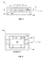
- FIG. 1 shows an exemplary ultra-high density data storage system 100 having electron emitters 102 and 104 and a phase-change data storage medium 106. Electron emitter 102 and 104 are mounted above the storage medium 106, that has a number of storage areas, such as 108, that are impacted by electron beams from the emitters.
- Micromovers based on micro-electromechanical systems (MEMS) technology, cause relative movement between the phase-change medium 106 and the electron emitters 102.
- Micromover 110 is connected to the storage medium 106 and moves it relative to the emitters 102, 104, so that each emitter can impact a number of different data storage areas.
- Figure 2 is a top view of the cross section A--A in Figure 1, showing the micro-mover 110 fabricated to scan the medium 106 in the X and Y directions.
- the storage medium 106 is supported two sets of thin-walled micro-fabricated flexible beams or springs 112 and 114 which flex to allow the medium 106 to move in the X direction with respect to a supporting frame 122.
- a second set of springs 116 and 118 are connected between the supporting frame 122 and the outer casing 120 and flex to allow the medium 106 and frame 122 to move in the Y direction with respect to the casing 120.
- the field emitters scan over the medium, or the medium scans over the field emitters in the X-Y directions by electrostatic, electromagnetic or piezoelectric means known in the art.
- FIG. 3 shows an exemplary diode structure 140 comprising the phase-change layer 106 described above and a second diode layer 142 forming a diode junction 144 at the interface of the two layers.
- phase-change layer 106 and second diode layer 142 have different electrical characteristics, to encourage the movement of carriers across the junction.
- phase change layer 106 may be n-type and second diode layer 142 may be p-type. Doping may be used to change or enhance the electrical characteristics of each layer.
- An external circuit 146 is connected to the diode to impress a voltage across the junction so as to create a bias, either in a reverse direction or in a forward direction, depending on the needs of the circuit.
- An output 148 is generated by circuit 146 and is representative of the magnitude of carrier flow across junction 144.
- Reading or detectingis carried out by directing a narrow beam of electrons 105 onto the surface of phase change layer 106 at data storage area 108.
- the incident electrons excite electron-hole pairs 107 near the surface of the storage area 108.
- the diode 140 is reversed-biased by external circuit 146 so that the minority carriers that are generated by the incident electrons drift toward the diode junction 144. Minority carriers that do not recombine with majority carriers before reaching the junction are swept across the junction, causing a current to flow in the external biasing circuit 146.
- a phase-change layer 202 is composed of indium and selenium in an indium selenide (InSe) compound which can be reversibly changed from an amorphous to a [GG5]crystalline state by heating and cooling the InSe compound at suitable rates. This state change is useful for data storage, since the amorphous state is less conductive that the crystalline state.
- the InSe compound may be any InSe-type material.
- InSe compound As used herein the terms "InSe compound,” “InSe-type material” and “InSe layer” mean any compound of InSe, In 2 Se 3 or a material in the group having the formula In X Se 1-X .
- the electrical properties of the InSe layer significantly change. Accordingly, the number of carriers swept across the diode junction will be significantly different in the amorphous state than when InSe is in a crystalline state.
- the second diode layer 204 is disposed below the phase-change layer 202 to form a diode junction 206. Since polycrystalline InSe-type materials are naturally n-type, the second diode layer 204 may be a p-type semiconductor layer or capable of being p-doped.
- the second diode layer 204 may be made of material of copper indium selenide (CuInSe), also known as CIS.
- CuInSe copper indium selenide
- CIS copper indium selenide
- CIS compound CIS compound
- CIS material refer to a material having any ratio of copper, indium, and selenium, such as CuInSe 2 , including but not limited to CIS doped with gallium (CIGS).
- CGS refers to CuInSe doped with gallium to form various stoichiometric materials of copper indium gallium selenide including but not limited to (Cu(In,Ga)Se 2 ) and Cu(In 1-x Ga x )Se 2 .
- CIS materials are desirable for memory diode materials for a number of-reasons.
- CIS compounds are similar to InSe-type materials, differing in the additional Cu element and a change in crystalline structure. Although the structures of these two compounds are different, the diode interface between layers of the two compounds is effective.
- CIS can be readily doped with a p-type dopant which is required to work with InSe.
- the CIS layer can be formed in the same vacuum system as an InSe layer, enabling the formation of a clean high quality interface between the two layers. This diode structure also reduces processing costs, since the time required for an additional fabrication stage is eliminated.
- CIS and CIGS materials tend to have relatively high melting temperatures, compared to InSe-type materials, so heat applied to the phase-change layer should not affect the CIS or CIGS layer.
- CIS materials tend to have good diode junction characteristics.
- the diode configuration 200 shown in Figure 4 may be used as a detection device in various data storage detection devices, such as photovoltaic devices, cathodovoltaic devices, photoluminescent devices and cathodoluminescent devices, all described above.
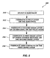
- Figure 5 discloses a method of fabrication 300 of the diode structure shown in Figure 4.
- Fabrication of the diode structure 200 starts at step 310 with the selection of a substrate layer 210 from silicon or various silicon oxide materials.
- substrate 210 is preferably of a material that can be doped with sodium, which promotes the growth of the subsequent layers. Such material includes, but is not limited to, silicon, silicon oxide, soda lime glass, and other semiconductor materials.
- an electrical potential field layer, or back contact, 208 is fabricated on the surface of substrate 210.
- Field layer 208 is fabricated from molybdenum (Mo) using a sputtering technique, known to those skilled in the art, to a thickness of 0.5-2.0 microns, with 1 micron being used in this embodiment.
- Mo molybdenum
- Other suitable conductive materials are indium, titanium nitride, platinum, gold, zinc oxide, indium tin oxide and/or nickel.
- second diode layer 204 is fabricated on field layer 208.
- diode layer 204 is preferably fabricated with a CIS compound and is doped with a p-type dopant.
- Second diode layer 204 has a thickness range of about 1 to 6 microns with 3.5 microns being used in this embodiment, and is applied by elemental evaporation in a vacuum.
- Other methods of fabrication can include sputtering or electrodeposition using an electrolyte of K 2 SO 4 , CuSO 4 , In 2 S(SO 4 ) 3 , and/or SeO 2 .
- second diode layer 204 may also be doped with gallium to form CuInGaSe 2 or other CIGS compounds.
- first diode layer 202 is fabricated on layer 208.
- first diode layer 202 is fabricated with In 2 Se 3 , being a natural n-type material.
- First layer 202 has a thickness range of 50-200 nm, with 100nm being used in this embodiment.
- First layer 202 may be applied by elemental evaporation in vacuum, which may be the same vacuum used to apply the second layer 204.
- fabrication of first layer 202 can be performed with electrodeposition using an electrolyte.
- layer 204 may be grown using a three-stage co-evaporation process.
- an (InGa) 2 Se 3 layer is deposited at 400°C, followed by evaporation of Cu and Se at 550°C to make the film slightly Cu-rich.
- the composition is restored to slightly Cu-poor by the addition of (InGa) 2 Se 3 again.
- the InSe layer is thermally evaporated from elemental sources onto a heated surface.
- InSe is a natural n-type material, so no doping is required.
- Cu can diffuse from the second diode layer of CuInSe into the InSe top layer to enhance the n-type doping.
- electric grid contacts 214 are fabricated on the surface of layer 202 because the first layer of InSe 202 has a low electrical conductivity.
- Contacts 214 are made of a conductive material the same as or similar to field layer 208.
- grid contacts 214 can be made of Mo at a thickness ranging from 0.5 to 5 microns, with 1 micron used in this embodiment.
- the grids may be made of other suitable materials, such as Au or In. The material may be sputter-deposited or made by any other suitable fabrication techniques known to those skilled in the art.
- Grid contacts 214 and Held layer 208 may be the connection points for applying a voltage source circuit to the diode 200 during a read operation.
- Testing has been performed on sample diodes as embodied in the present invention. The tests have included measuring the I-V characteristics of the diodes, performing quantum efficiency (optical), and performing electron beam induced current (EBIC) measurements, which simulate a "read" mode for data storage.
- quantum efficiency optical
- EBIC electron beam induced current
- Figure 6 contains bar graphs showing EBIC gain as a function of emitter beam voltage for diodes having In 2 Se 3 as the top layer with In or Au contacts and Si or CIGS as a bottom layer.
- the EBIC gain is diode current output divided by electron beam current.
- In 2 Se 3 was applied after the substrate was exposed to air.
- the second two samples (in situ) were fabricated by depositing both layers in a vacuum without exposure to air during the process.
- the EBIC variations are not linear with variations in emitter beam energy, because more energetic electron beams result in both more electron-hole pairs and deeper penetration. Although 5 kV beams may be used, beams of 1 kV or less may be utilized in most applications. Beam current may vary from 0.5 nA to as high as 200 nA, with about 20 nA being used in some applications. As seen from the graph, EBIC gain is considerably better with CIGS rather than Si as a bottom diode layer. Also, the gain is substantially higher if the diode is fabricated in a vacuum.
- Figure 7 shows the current-voltage characteristics for three samples of the first diode listed in Figure 6. As shown in Figure 7, the applied voltage causes essentially zero current until it reaches about 200 mV, after which there is a sharp increase in current.
- the open circuit voltage is 5 mV and the short circuit current density is about 2 to 3 mA cm 2 .
Landscapes
- Engineering & Computer Science (AREA)
- Physics & Mathematics (AREA)
- Chemical & Material Sciences (AREA)
- Nanotechnology (AREA)
- Plasma & Fusion (AREA)
- Mathematical Physics (AREA)
- Theoretical Computer Science (AREA)
- Crystallography & Structural Chemistry (AREA)
- Semiconductor Memories (AREA)
- Static Random-Access Memory (AREA)
Abstract
Description
- The present invention relates to ultra-high density data storage devices, in the preferred embodiments to ultra-high density storage devices having diode memory cells using materials containing copper, indium, and selenium, and methods of fabricating the diode memory cells.
- Electronic devices, such as palm computers, digital cameras and cellular telephones, are becoming more compact and miniature, even as they incorporate more sophisticated data processing and storage circuitry. Moreover, types of digital communication other than text are becoming much more common, such as video, audio and graphics, requiring massive amounts of data to convey the complex information inherent therein. These developments have created an enormous demand for new storage technologies that are capable of handling more complex data at a lower cost and in a much more compact package. Efforts are now underway to enable the storage of data on a scale of ten nanometers (100 angstroms) up to hundreds of nanometers, referred to herein as "ultra-high density data storage."
- One method of storing data at ultra-high densities involves utilizing a directed energy beam. As used herein a "directed energy beam" means a beam of particles, such as electrons, or a beam of photons or other electromagnetic energy, to heat the [GG1]medium so that it changes states[GG2][GG3]. As used herein, "state" is defined broadly to include any type of physical change of a material, whether from one form to another, such as crystalline to amorphous, or from one structure or phase to another, such as different crystalline structures. As used herein, the term "phase change" means a change between different states in a material.
- A state change may be accomplished by changing a material from crystalline to amorphous, or the reverse, by the application of an electron or light beam. To change from the amorphous to crystalline state, beam power density is increased so as to locally heat the medium to a crystallization temperature [GG4]. The beam is left on long enough to allow the medium to anneal into its crystalline state. To change from crystalline to amorphous state, the beam power density is increased to a level high enough to locally melt the medium and then rapidly decreased so as to allow the medium to cool before it can reanneal. To read from the storage medium, a lower-energy beam is directed to the storage area to cause activity, such as current flow representative of the state of the storage area.
- To effectively sense contrasts in states or phases of phase-change materials, a diode may be formedhaving a junction for sensing carrier flow in response to an electron or light beam focused on a data storage memory cell in the phase-change layer. Such diode junctions are utilized for carrier detection in photovoltaic devices, in which light beams impact the diode, and in cathodovoltaic devices, in which electron beams are directed to the diode. Photovoltaic devices include phototransistor devices and photodiode devices. Cathodovoltaic devices include cathodotransistor devices and cathododiode devices. In addition, diode junctions may be utilized for carrier flow detection in photoluminescent and cathodoluminescent devices. Reference is made to copending patent
application serial number 10/286,010 [HP 20020-6667] filed on October 31, 2002 for further description of the structure and function of diode junctions in these devices. - The present invention seeks to provide an improved data storage device.
- According to an aspect of the present invention, there is provided an ultra-high density data storage device as specified in
claim 1. - Diode junction layers need to be composed of materials having electrical properties suitable for generating a desired carrier flow across the diode junction. As used herein, the term "carrier flow" refers to either electron current or the flow of holes, depending on whether the materials are n-type or p-type. As used herein, the term "materials" includes all kinds and types of compounds, alloys and other combinations of elements. Various types of junctions may be formed in the context of the above data storage devices, such as heterojunctions, homojunctions, and Schottky junctions, in order to achieve the desired detection results.
- One embodiment comprises an ultra-high density data storage device using phase-change diode memory cells, and having a plurality of emitters for directing beams of directed energy, a layer for forming multiple data storage cells and a layered diode structure for detecting a memory or data state of the storage cells, wherein the device comprises a phase-change data storage layer capable of changing states in response to the beams from the emitters, and a second layer forming one layer in the layered diode structure, the structure layer comprising a material containing copper, indium and selenium.
- Another output provides a method of forming a diode structure for a phase-change data storage array, having multiple thin film layers adapted to form a plurality of data storage cell diodes, wherein the method comprises depositing a first diode layer of CIS material on a substrate and depositing a second diode layer of phase-change material on the first diode layer.
- Embodiments of the present invention are described below, by way of example only, with reference to the accompanying drawings in which:
- Figure 1 is a partial side view of an exemplary data storage system;
- Figure 2 is a plan view of the storage system shown in Figure 1;
- Figure 3 is a schematic view of a portion of the storage system shown in Figure 1;
- Figure 4 is a schematic side view of the diode structure according to one embodiment of the present invention;
- Figure 5 is a flow chart describing a method for fabricating the diode structure shown in Figure 4;
- Figure 6 is a bar graph showing EBIC diode characteristics according to four diode embodiments of the present invention; and
- Figure 7 is a graph showing the current-voltage characteristics of a diode according to one of the embodiments of Figure 6.
-
- Reference will now be made to the exemplary embodiments illustrated in the drawings, and specific language will be used herein to describe the same. It will nevertheless be understood that no limitation of the scope of the invention is thereby intended. Alterations and further modifications of the features illustrated herein, and additional applications of the principles illustrated herein, which would occur to one skilled in the relevant art and having possession of this disclosure, are to be considered within the scope of the claims.
Figure 1 shows an exemplary ultra-high densitydata storage system 100 havingelectron emitters data storage medium 106.Electron emitter storage medium 106, that has a number of storage areas, such as 108, that are impacted by electron beams from the emitters. Micromovers, based on micro-electromechanical systems (MEMS) technology, cause relative movement between the phase-change medium 106 and theelectron emitters 102. Micromover 110 is connected to thestorage medium 106 and moves it relative to theemitters medium 106 in the X and Y directions. Thestorage medium 106 is supported two sets of thin-walled micro-fabricated flexible beams orsprings 112 and 114 which flex to allow themedium 106 to move in the X direction with respect to a supportingframe 122. A second set ofsprings frame 122 and theouter casing 120 and flex to allow themedium 106 andframe 122 to move in the Y direction with respect to thecasing 120. The field emitters scan over the medium, or the medium scans over the field emitters in the X-Y directions by electrostatic, electromagnetic or piezoelectric means known in the art. - Figure 3 shows an
exemplary diode structure 140 comprising the phase-change layer 106 described above and asecond diode layer 142 forming adiode junction 144 at the interface of the two layers. Typically, phase-change layer 106 andsecond diode layer 142 have different electrical characteristics, to encourage the movement of carriers across the junction. For example,phase change layer 106 may be n-type andsecond diode layer 142 may be p-type. Doping may be used to change or enhance the electrical characteristics of each layer. Anexternal circuit 146 is connected to the diode to impress a voltage across the junction so as to create a bias, either in a reverse direction or in a forward direction, depending on the needs of the circuit. Anoutput 148 is generated bycircuit 146 and is representative of the magnitude of carrier flow acrossjunction 144. - Reading or detectingis carried out by directing a narrow beam of
electrons 105 onto the surface ofphase change layer 106 atdata storage area 108. The incident electrons excite electron-hole pairs 107 near the surface of thestorage area 108. Thediode 140 is reversed-biased byexternal circuit 146 so that the minority carriers that are generated by the incident electrons drift toward thediode junction 144. Minority carriers that do not recombine with majority carriers before reaching the junction are swept across the junction, causing a current to flow in theexternal biasing circuit 146. - Writing onto
diode 140 is accomplished by increasing the power density of theelectron beam 105 enough to locally alter some property of the diode atstorage area 108, such as collection efficiency of minority carriers. In Figure 4, a schematic side view of adiode configuration 200 in accordance with one embodiment of the present invention is shown. A phase-change layer 202 is composed of indium and selenium in an indium selenide (InSe) compound which can be reversibly changed from an amorphous to a [GG5]crystalline state by heating and cooling the InSe compound at suitable rates. This state change is useful for data storage, since the amorphous state is less conductive that the crystalline state. The InSe compound may be any InSe-type material. As used herein the terms "InSe compound," "InSe-type material" and "InSe layer" mean any compound of InSe, In2Se3 or a material in the group having the formula InXSe1-X. - When the InSe
layer 202 is changed from the crystalline state to the amorphous state at thestorage area 212, the electrical properties of the InSe layer significantly change. Accordingly, the number of carriers swept across the diode junction will be significantly different in the amorphous state than when InSe is in a crystalline state. - In Figure 4, the
second diode layer 204 is disposed below the phase-change layer 202 to form adiode junction 206. Since polycrystalline InSe-type materials are naturally n-type, thesecond diode layer 204 may be a p-type semiconductor layer or capable of being p-doped. Thesecond diode layer 204 may be made of material of copper indium selenide (CuInSe), also known as CIS. The terms "CIS," "CIS compound" or "CIS material" refer to a material having any ratio of copper, indium, and selenium, such as CuInSe2, including but not limited to CIS doped with gallium (CIGS). The term "CIGS" refers to CuInSe doped with gallium to form various stoichiometric materials of copper indium gallium selenide including but not limited to (Cu(In,Ga)Se2) and Cu(In1-xGax)Se2. - CIS materials are desirable for memory diode materials for a number of-reasons. CIS compounds are similar to InSe-type materials, differing in the additional Cu element and a change in crystalline structure. Although the structures of these two compounds are different, the diode interface between layers of the two compounds is effective. Also, CIS can be readily doped with a p-type dopant which is required to work with InSe. Further, the CIS layer can be formed in the same vacuum system as an InSe layer, enabling the formation of a clean high quality interface between the two layers. This diode structure also reduces processing costs, since the time required for an additional fabrication stage is eliminated. In addition, CIS and CIGS materials tend to have relatively high melting temperatures, compared to InSe-type materials, so heat applied to the phase-change layer should not affect the CIS or CIGS layer. Finally, CIS materials tend to have good diode junction characteristics.
- The
diode configuration 200 shown in Figure 4 may be used as a detection device in various data storage detection devices, such as photovoltaic devices, cathodovoltaic devices, photoluminescent devices and cathodoluminescent devices, all described above. - Figure 5 discloses a method of
fabrication 300 of the diode structure shown in Figure 4. Fabrication of thediode structure 200 starts atstep 310 with the selection of asubstrate layer 210 from silicon or various silicon oxide materials. In the present embodiment,substrate 210 is preferably of a material that can be doped with sodium, which promotes the growth of the subsequent layers. Such material includes, but is not limited to, silicon, silicon oxide, soda lime glass, and other semiconductor materials. Atstep 312, an electrical potential field layer, or back contact, 208 is fabricated on the surface ofsubstrate 210.Field layer 208 is fabricated from molybdenum (Mo) using a sputtering technique, known to those skilled in the art, to a thickness of 0.5-2.0 microns, with 1 micron being used in this embodiment. Other suitable conductive materials are indium, titanium nitride, platinum, gold, zinc oxide, indium tin oxide and/or nickel. - Next, at
step 314,second diode layer 204 is fabricated onfield layer 208. Other suitable phase-change materials may be used. In this embodiment,diode layer 204 is preferably fabricated with a CIS compound and is doped with a p-type dopant.Second diode layer 204 has a thickness range of about 1 to 6 microns with 3.5 microns being used in this embodiment, and is applied by elemental evaporation in a vacuum. Other methods of fabrication can include sputtering or electrodeposition using an electrolyte of K2SO4, CuSO4, In2S(SO4)3, and/or SeO2. As previously mentioned,second diode layer 204 may also be doped with gallium to form CuInGaSe2 or other CIGS compounds. - At
step 316, after application of thesecond diode layer 204, thefirst diode layer 202 is fabricated onlayer 208. In the present embodiment,first diode layer 202 is fabricated with In2Se3, being a natural n-type material.First layer 202 has a thickness range of 50-200 nm, with 100nm being used in this embodiment.First layer 202 may be applied by elemental evaporation in vacuum, which may be the same vacuum used to apply thesecond layer 204. In an alternative embodiment, fabrication offirst layer 202 can be performed with electrodeposition using an electrolyte. - In an embodiment in which
layer 204 is a CIGS material,layer 204 may be grown using a three-stage co-evaporation process. First, an (InGa)2Se3 layer is deposited at 400°C, followed by evaporation of Cu and Se at 550°C to make the film slightly Cu-rich. The composition is restored to slightly Cu-poor by the addition of (InGa)2Se3 again. Next, the InSe layer is thermally evaporated from elemental sources onto a heated surface. InSe is a natural n-type material, so no doping is required. Further, Cu can diffuse from the second diode layer of CuInSe into the InSe top layer to enhance the n-type doping. - At
step 318,electric grid contacts 214 are fabricated on the surface oflayer 202 because the first layer ofInSe 202 has a low electrical conductivity.Contacts 214 are made of a conductive material the same as or similar tofield layer 208. For example,grid contacts 214 can be made of Mo at a thickness ranging from 0.5 to 5 microns, with 1 micron used in this embodiment. Alternately, the grids may be made of other suitable materials, such as Au or In. The material may be sputter-deposited or made by any other suitable fabrication techniques known to those skilled in the art.Grid contacts 214 and Heldlayer 208 may be the connection points for applying a voltage source circuit to thediode 200 during a read operation. - Testing has been performed on sample diodes as embodied in the present invention. The tests have included measuring the I-V characteristics of the diodes, performing quantum efficiency (optical), and performing electron beam induced current (EBIC) measurements, which simulate a "read" mode for data storage.
- Figure 6 contains bar graphs showing EBIC gain as a function of emitter beam voltage for diodes having In2Se3 as the top layer with In or Au contacts and Si or CIGS as a bottom layer. The EBIC gain is diode current output divided by electron beam current. In the first two samples, In2Se3 was applied after the substrate was exposed to air. The second two samples (in situ) were fabricated by depositing both layers in a vacuum without exposure to air during the process.
- As shown in the Figure 6 graph, the EBIC variations are not linear with variations in emitter beam energy, because more energetic electron beams result in both more electron-hole pairs and deeper penetration. Although 5 kV beams may be used, beams of 1 kV or less may be utilized in most applications. Beam current may vary from 0.5 nA to as high as 200 nA, with about 20 nA being used in some applications. As seen from the graph, EBIC gain is considerably better with CIGS rather than Si as a bottom diode layer. Also, the gain is substantially higher if the diode is fabricated in a vacuum.
- Figure 7 shows the current-voltage characteristics for three samples of the first diode listed in Figure 6. As shown in Figure 7, the applied voltage causes essentially zero current until it reaches about 200 mV, after which there is a sharp increase in current. The open circuit voltage is 5 mV and the short circuit current density is about 2 to 3 mA cm2.
- It is to be understood that the above-referenced arrangements are illustrative of the application for the principles taught herein. Numerous modifications and alternative arrangements can be devised without departing from the scope of the claims.
- The disclosures in United States patent application no. 10/654,189, from which this application claims priority, and in the abstract accompanying this application are incorporated herein by reference.
Claims (10)
- An ultra-high density storage device (200) using phase-change diode memory cells, and including a plurality of emitters (102, 104) for directing beams (105) of directed energy, a layer (202) for forming multiple data storage cells and a layered diode structure (202, 204) for detecting a memory or data state of the storage cells, the device including:a phase-change data storage layer (202) capable of changing states in response to beams (105) from the emitters (102, 104); anda second layer (204) forming one layer in the layered diode structure (202, 204), the second layer (204) comprising a material containing copper, indium and selenium.
- A storage device according to claim 1, wherein the material comprising the second layer (204) is a CuInSe material doped with gallium.
- A storage device according to claim 1 or 2, wherein the second layer (204) is doped with a p-type dopant.
- A storage device according to claim 1, 2 or 3, wherein the phase-change data storage layer (202) and the second layer (204) form the layered diode structure (202, 204).
- A storage device according to any preceding claim, wherein the phase-change layer (204) comprises an indium selenide material.
- A storage device according to any preceding claim, wherein the diode structure (200) is a detection element in one of a group of data storage detection devices, selected from the group of photovoltaic devices, cathodevoltaic devices, photoluminescent devices and cathodoluminescent devices.
- A method of forming a diode structure (200) for a phase-change data storage array, provided with a multiple thin film layers (202, 204) adapted to form a plurality of data storage cell diodes, including:depositing a first diode layer (204) of CuInSe material on a substrate; anddepositing a second diode layer (202) of phase-change material on the first diode layer (204).
- A method according to claim 7, including doping the layer (204) of CuInSe material with gallium.
- A method according to claim 7 or 8, wherein the steps of depositing the first diode layer (204) and the second diode layer (202) are done in the same vacuum system.
- A method according to claim 7, 8 or 9, wherein the steps of depositing the first diode layer (204) and the second diode layer (202) are done by an electrodeposition process.
Applications Claiming Priority (2)
| Application Number | Priority Date | Filing Date | Title |
|---|---|---|---|
| US654189 | 2003-09-03 | ||
| US10/654,189 US6979838B2 (en) | 2003-09-03 | 2003-09-03 | Ultra-high density storage device using phase change diode memory cells and methods of fabrication thereof |
Publications (2)
| Publication Number | Publication Date |
|---|---|
| EP1517318A1 true EP1517318A1 (en) | 2005-03-23 |
| EP1517318B1 EP1517318B1 (en) | 2007-06-27 |
Family
ID=34194679
Family Applications (1)
| Application Number | Title | Priority Date | Filing Date |
|---|---|---|---|
| EP04254527A Expired - Lifetime EP1517318B1 (en) | 2003-09-03 | 2004-07-28 | Ultra-high density data storage device |
Country Status (4)
| Country | Link |
|---|---|
| US (2) | US6979838B2 (en) |
| EP (1) | EP1517318B1 (en) |
| JP (1) | JP3723817B2 (en) |
| DE (1) | DE602004007208T2 (en) |
Families Citing this family (9)
| Publication number | Priority date | Publication date | Assignee | Title |
|---|---|---|---|---|
| US20040218499A1 (en) * | 2003-05-01 | 2004-11-04 | Alison Chaiken | Ultra-high density storage and retrieval device using ordered-defect materials and methods of fabrication thereof |
| SE0301350D0 (en) * | 2003-05-08 | 2003-05-08 | Forskarpatent I Uppsala Ab | A thin-film solar cell |
| US7057202B2 (en) * | 2003-09-26 | 2006-06-06 | Hewlett-Packard Development Company, L.P. | Ultra-high density storage device using phase change diode memory cells and methods of fabrication thereof |
| US7306963B2 (en) * | 2004-11-30 | 2007-12-11 | Spire Corporation | Precision synthesis of quantum dot nanostructures for fluorescent and optoelectronic devices |
| US7514725B2 (en) * | 2004-11-30 | 2009-04-07 | Spire Corporation | Nanophotovoltaic devices |
| CN102034896B (en) * | 2009-09-28 | 2015-03-11 | 思阳公司 | Self-cleaning large-scale method for selenylation of a thin film photovoltaic material |
| US8284597B2 (en) | 2010-05-06 | 2012-10-09 | Macronix International Co., Ltd. | Diode memory |
| US10580976B2 (en) | 2018-03-19 | 2020-03-03 | Sandisk Technologies Llc | Three-dimensional phase change memory device having a laterally constricted element and method of making the same |
| CN112464156B (en) * | 2020-12-17 | 2022-08-23 | 长江先进存储产业创新中心有限责任公司 | Matrix and vector multiplication method and device |
Citations (5)
| Publication number | Priority date | Publication date | Assignee | Title |
|---|---|---|---|---|
| US3983542A (en) * | 1970-08-13 | 1976-09-28 | Energy Conversion Devices, Inc. | Method and apparatus for recording information |
| US5557596A (en) * | 1995-03-20 | 1996-09-17 | Gibson; Gary | Ultra-high density storage device |
| US20020176349A1 (en) * | 2001-05-25 | 2002-11-28 | Gibson Gary A. | Data storage medium utilizing directed light beam and near-field optical sources |
| US20030081527A1 (en) * | 2001-10-31 | 2003-05-01 | Gibson Gary A. | Data storage media and methods utilizing a layer adjacent the storage layer |
| US20040086802A1 (en) * | 2002-10-31 | 2004-05-06 | Gibson Gary A. | Two-dimensional materials and methods for ultra-high density data storage and retrieval |
Family Cites Families (5)
| Publication number | Priority date | Publication date | Assignee | Title |
|---|---|---|---|---|
| US5254480A (en) * | 1992-02-20 | 1993-10-19 | Minnesota Mining And Manufacturing Company | Process for producing a large area solid state radiation detector |
| US6256224B1 (en) * | 2000-05-03 | 2001-07-03 | Hewlett-Packard Co | Write circuit for large MRAM arrays |
| US6784361B2 (en) * | 2000-09-20 | 2004-08-31 | Bp Corporation North America Inc. | Amorphous silicon photovoltaic devices |
| US6900468B2 (en) * | 2001-02-20 | 2005-05-31 | Hewlett-Packard Development Company, L.P. | Indium chalcogenide, gallium chalcogenide, and indium-gallium chalcogenide phase-change media for ultra-high-density data-storage devices |
| US20040218499A1 (en) * | 2003-05-01 | 2004-11-04 | Alison Chaiken | Ultra-high density storage and retrieval device using ordered-defect materials and methods of fabrication thereof |
-
2003
- 2003-09-03 US US10/654,189 patent/US6979838B2/en not_active Expired - Fee Related
-
2004
- 2004-07-28 EP EP04254527A patent/EP1517318B1/en not_active Expired - Lifetime
- 2004-07-28 DE DE602004007208T patent/DE602004007208T2/en not_active Expired - Fee Related
- 2004-09-03 JP JP2004256801A patent/JP3723817B2/en not_active Expired - Fee Related
-
2005
- 2005-10-17 US US11/253,233 patent/US7151008B2/en not_active Expired - Fee Related
Patent Citations (5)
| Publication number | Priority date | Publication date | Assignee | Title |
|---|---|---|---|---|
| US3983542A (en) * | 1970-08-13 | 1976-09-28 | Energy Conversion Devices, Inc. | Method and apparatus for recording information |
| US5557596A (en) * | 1995-03-20 | 1996-09-17 | Gibson; Gary | Ultra-high density storage device |
| US20020176349A1 (en) * | 2001-05-25 | 2002-11-28 | Gibson Gary A. | Data storage medium utilizing directed light beam and near-field optical sources |
| US20030081527A1 (en) * | 2001-10-31 | 2003-05-01 | Gibson Gary A. | Data storage media and methods utilizing a layer adjacent the storage layer |
| US20040086802A1 (en) * | 2002-10-31 | 2004-05-06 | Gibson Gary A. | Two-dimensional materials and methods for ultra-high density data storage and retrieval |
Also Published As
| Publication number | Publication date |
|---|---|
| DE602004007208T2 (en) | 2008-02-28 |
| JP3723817B2 (en) | 2005-12-07 |
| EP1517318B1 (en) | 2007-06-27 |
| US7151008B2 (en) | 2006-12-19 |
| US20050048733A1 (en) | 2005-03-03 |
| DE602004007208D1 (en) | 2007-08-09 |
| US6979838B2 (en) | 2005-12-27 |
| US20060030068A1 (en) | 2006-02-09 |
| JP2005078797A (en) | 2005-03-24 |
Similar Documents
| Publication | Publication Date | Title |
|---|---|---|
| Gibson et al. | Phase-change recording medium that enables ultrahigh-density electron-beam data storage | |
| US7052757B2 (en) | Capping layer for enhanced performance media | |
| Aranovich et al. | Photovoltaic properties of ZnO/CdTe heterojunctions prepared by spray pyrolysis | |
| Dullweber et al. | Photogeneration and carrier recombination in graded gap Cu (In, Ga) Se/sub 2/solar cells | |
| US20040086802A1 (en) | Two-dimensional materials and methods for ultra-high density data storage and retrieval | |
| Dharmadasa et al. | Perovskite solar cells: short lifetime and hysteresis behaviour of current–voltage characteristics | |
| US6900468B2 (en) | Indium chalcogenide, gallium chalcogenide, and indium-gallium chalcogenide phase-change media for ultra-high-density data-storage devices | |
| JP2003062800A (en) | Device separation process flow for ARS system | |
| EP1517318B1 (en) | Ultra-high density data storage device | |
| US7057202B2 (en) | Ultra-high density storage device using phase change diode memory cells and methods of fabrication thereof | |
| Broudy et al. | (HgCd) Te photoconductive detectors | |
| US4297717A (en) | Semiconductor device | |
| Raissi et al. | Highly sensitive ptsi/porous si schottky detectors | |
| US20040218499A1 (en) | Ultra-high density storage and retrieval device using ordered-defect materials and methods of fabrication thereof | |
| KR102019599B1 (en) | Graphene based photodiode and method of manufacturing the same | |
| JP5382696B2 (en) | Semiconductor optical device and semiconductor solar cell | |
| US4412235A (en) | Integrated opto-electronic relay using a semiconductor with persistent photoconductivity and a matrix of such relays | |
| Hood et al. | LWIR high performance focal plane arrays based on type-II strained layer superlattice (SLS) materials | |
| JPH09307133A (en) | Photodiode and its manufacture | |
| Chaiken et al. | Electron-beam detection of bits reversibly recorded on epitaxial InSe/GaSe/Si phase-change diodes | |
| Dixit | Transient Investigations of Hot-Carrier Dynamics in the Solar-Absorber Material AlInAs | |
| Nathan et al. | Type II superlattice infrared detector and focal plane arrays | |
| BUBE et al. | density npo and the lifetime of minority carriers τη | |
| Jiang | Theoretical and experimental study of energy selective contacts for hot carrier solar cells and extensions to tandem cells | |
| US7082095B2 (en) | System and method for storing data |
Legal Events
| Date | Code | Title | Description |
|---|---|---|---|
| PUAI | Public reference made under article 153(3) epc to a published international application that has entered the european phase |
Free format text: ORIGINAL CODE: 0009012 |
|
| AK | Designated contracting states |
Kind code of ref document: A1 Designated state(s): AT BE BG CH CY CZ DE DK EE ES FI FR GB GR HU IE IT LI LU MC NL PL PT RO SE SI SK TR |
|
| AX | Request for extension of the european patent |
Extension state: AL HR LT LV MK |
|
| RIN1 | Information on inventor provided before grant (corrected) |
Inventor name: ASHTON, GARY R. Inventor name: GIBSON, GARY A. Inventor name: BICKNELL-TASSIUS, ROBERT N. |
|
| 17P | Request for examination filed |
Effective date: 20050915 |
|
| AKX | Designation fees paid |
Designated state(s): DE GB IT |
|
| GRAP | Despatch of communication of intention to grant a patent |
Free format text: ORIGINAL CODE: EPIDOSNIGR1 |
|
| GRAS | Grant fee paid |
Free format text: ORIGINAL CODE: EPIDOSNIGR3 |
|
| GRAA | (expected) grant |
Free format text: ORIGINAL CODE: 0009210 |
|
| AK | Designated contracting states |
Kind code of ref document: B1 Designated state(s): DE GB IT |
|
| REG | Reference to a national code |
Ref country code: GB Ref legal event code: FG4D |
|
| REF | Corresponds to: |
Ref document number: 602004007208 Country of ref document: DE Date of ref document: 20070809 Kind code of ref document: P |
|
| PLBE | No opposition filed within time limit |
Free format text: ORIGINAL CODE: 0009261 |
|
| STAA | Information on the status of an ep patent application or granted ep patent |
Free format text: STATUS: NO OPPOSITION FILED WITHIN TIME LIMIT |
|
| 26N | No opposition filed |
Effective date: 20080328 |
|
| PGFP | Annual fee paid to national office [announced via postgrant information from national office to epo] |
Ref country code: DE Payment date: 20090729 Year of fee payment: 6 Ref country code: GB Payment date: 20090727 Year of fee payment: 6 |
|
| PGFP | Annual fee paid to national office [announced via postgrant information from national office to epo] |
Ref country code: IT Payment date: 20090727 Year of fee payment: 6 |
|
| GBPC | Gb: european patent ceased through non-payment of renewal fee |
Effective date: 20100728 |
|
| PG25 | Lapsed in a contracting state [announced via postgrant information from national office to epo] |
Ref country code: DE Free format text: LAPSE BECAUSE OF NON-PAYMENT OF DUE FEES Effective date: 20110201 |
|
| REG | Reference to a national code |
Ref country code: DE Ref legal event code: R119 Ref document number: 602004007208 Country of ref document: DE Effective date: 20110201 |
|
| PG25 | Lapsed in a contracting state [announced via postgrant information from national office to epo] |
Ref country code: IT Free format text: LAPSE BECAUSE OF NON-PAYMENT OF DUE FEES Effective date: 20100728 |
|
| PG25 | Lapsed in a contracting state [announced via postgrant information from national office to epo] |
Ref country code: GB Free format text: LAPSE BECAUSE OF NON-PAYMENT OF DUE FEES Effective date: 20100728 |