EP1512123B1 - System and method for electronic correction of optical anomalies - Google Patents
System and method for electronic correction of optical anomalies Download PDFInfo
- Publication number
- EP1512123B1 EP1512123B1 EP03759800A EP03759800A EP1512123B1 EP 1512123 B1 EP1512123 B1 EP 1512123B1 EP 03759800 A EP03759800 A EP 03759800A EP 03759800 A EP03759800 A EP 03759800A EP 1512123 B1 EP1512123 B1 EP 1512123B1
- Authority
- EP
- European Patent Office
- Prior art keywords
- optical
- anomaly
- correcting
- image
- transformation
- Prior art date
- Legal status (The legal status is an assumption and is not a legal conclusion. Google has not performed a legal analysis and makes no representation as to the accuracy of the status listed.)
- Expired - Lifetime
Links
- 230000003287 optical effect Effects 0.000 title claims abstract description 136
- 238000012937 correction Methods 0.000 title claims abstract description 58
- 238000000034 method Methods 0.000 title claims abstract description 26
- 230000009466 transformation Effects 0.000 claims abstract description 105
- 238000000844 transformation Methods 0.000 claims abstract description 59
- 230000006870 function Effects 0.000 claims description 27
- 238000001914 filtration Methods 0.000 claims description 12
- 230000004075 alteration Effects 0.000 abstract description 40
- 230000000694 effects Effects 0.000 abstract description 17
- 230000008569 process Effects 0.000 abstract description 3
- 230000003044 adaptive effect Effects 0.000 abstract description 2
- 238000013507 mapping Methods 0.000 description 36
- 238000012545 processing Methods 0.000 description 27
- 239000003086 colorant Substances 0.000 description 12
- 230000006399 behavior Effects 0.000 description 9
- 238000010586 diagram Methods 0.000 description 8
- 230000008859 change Effects 0.000 description 7
- 230000001419 dependent effect Effects 0.000 description 5
- 239000013598 vector Substances 0.000 description 5
- 238000013459 approach Methods 0.000 description 4
- 230000007547 defect Effects 0.000 description 4
- 230000008901 benefit Effects 0.000 description 3
- 239000000203 mixture Substances 0.000 description 3
- 241000226585 Antennaria plantaginifolia Species 0.000 description 2
- 206010010071 Coma Diseases 0.000 description 2
- XUIMIQQOPSSXEZ-UHFFFAOYSA-N Silicon Chemical compound [Si] XUIMIQQOPSSXEZ-UHFFFAOYSA-N 0.000 description 2
- 201000009310 astigmatism Diseases 0.000 description 2
- 230000015572 biosynthetic process Effects 0.000 description 2
- 239000004926 polymethyl methacrylate Substances 0.000 description 2
- 229910052710 silicon Inorganic materials 0.000 description 2
- 239000010703 silicon Substances 0.000 description 2
- 230000006978 adaptation Effects 0.000 description 1
- 238000006243 chemical reaction Methods 0.000 description 1
- 238000000576 coating method Methods 0.000 description 1
- 239000012141 concentrate Substances 0.000 description 1
- 239000006185 dispersion Substances 0.000 description 1
- 238000011156 evaluation Methods 0.000 description 1
- 239000000463 material Substances 0.000 description 1
- 238000013178 mathematical model Methods 0.000 description 1
- 238000012986 modification Methods 0.000 description 1
- 230000004048 modification Effects 0.000 description 1
- 238000005457 optimization Methods 0.000 description 1
- 230000004044 response Effects 0.000 description 1
- 238000005070 sampling Methods 0.000 description 1
- 238000012360 testing method Methods 0.000 description 1
- 230000007704 transition Effects 0.000 description 1
Images


Classifications
-
- G06T3/047—
-
- G—PHYSICS
- G06—COMPUTING; CALCULATING OR COUNTING
- G06T—IMAGE DATA PROCESSING OR GENERATION, IN GENERAL
- G06T3/00—Geometric image transformation in the plane of the image
-
- G—PHYSICS
- G06—COMPUTING; CALCULATING OR COUNTING
- G06T—IMAGE DATA PROCESSING OR GENERATION, IN GENERAL
- G06T5/00—Image enhancement or restoration
-
- G06T5/80—
Definitions
- This invention relates to electronic correction of optical anomalies and more particularly to electronic correction of distortion, lateral chromatic aberration, luminance non-uniformity,and chrominance non-uniformity, which can be combined with a general image transform (e.g. scaling and geometric transform).
- a general image transform e.g. scaling and geometric transform
- optical anomalies are inherent to the non-ideal behavior of the various optical elements and to accuracy and tolerance of assembly.
- Various components sensors, displays, lens, prisms, mirrors, light source
- optical or otherwise and their orientation may introduce their own specific optical anomalies, such as distortion, tilt, lateral chromatic aberration, luminance or chrominance non-uniformity.
- optical aberration is generally used to refer to any effect that leads to an non-ideal image formation..
- Optical aberrations include diffraction effects (due to the wave nature of light), chromatic aberrations (caused by optical dispersion, or the differences in refraction in different wavelengths of light), and monochromatic aberrations (of which spherical aberration, coma, and astigmatism are concerned with failures of a point object to form a point image, and field curvature and distortion are concerned with the failure of finite objects perpendicular to the principal axis to form a well-focused plane image).
- spherical aberration, coma, and astigmatism are concerned with failures of a point object to form a point image
- field curvature and distortion are concerned with the failure of finite objects perpendicular to the principal axis to form a well-focused plane image.
- the former types degrade the sharpness of an image, that is, the image appears blurred, and/or out of focus, and/or has color fringes.
- Aberrations in this category include spherical aberrations, astigmatism, coma, field of curvature and axial chromatic aberration.
- the latter types of aberrations affect the shape of the image that in part may be induced by the former aberration or by the correction and optimization of the former aberration. In this case, points in the object plane are shifted or distorted in comparison with an ideal mapping in the image plane. In an ideal mapping an object in the image plane will appear as it does in the object plane, with possibly a uniform scale change. For example, an image may appear curved near the edges or appear rotated.
- Aberrations in this second category include distortions (e.g. pincushion/barrel effects) and lateral chromatic aberrations.
- chromatic aberrations With the exception of chromatic aberrations, all other optical aberrations are present in monochromatic (i.e. single color) light. Chromatic aberration appears when dealing with polychromatic light (many colors). In short, the index of refraction is wavelength dependent, which means that the red, green and blue components bend differently at an optical interface. This leads to axial (longitudinal) and/or lateral chromatic aberration effects. In axial chromatic aberration, the three components are brought to focus on different planes in the image space, which gives a color blurring effect. In other words, axial chromatic aberration arises due to the focal length varying with wavelength (color).
- lateral chromatic aberration color components from a single point are brought to focus to different points on the same image plane. This has the effect of magnifying the three colors differently and can be visually seen as 'color fringing'. Thus lateral chromatic aberration can be seen as an effect due to magnification varying with wavelength.
- the three colors can also mismatch due to non-optical effects.
- color non-convergence is used to refer to color mismatch effects, whether optical (as in chromatic aberrations) or not. Further discussion on optical aberrations can be found in conventional optics textbooks, such as Robert Guenther's Modern Optics, published by John Wiley & Sons, 1990 .
- Luminance non-uniformity leads to varying brightness across an image.
- Common causes include a varying (in brightness) light source, varying optical path across the image plane, non-uniform sensor response and irregularities in panels (e.g. LCD, LCOS, etc.). Both large-scale and small-scale non-uniformities can be present.
- brightness variation can be different for each color, leading to chrominance non-uniformity.
- lateral chromatic aberration is commonly corrected (or minimized) using special optical elements, often consisting of prism/lens combinations and/or special material coatings such as that disclosed in U.S. Patent Nos. 4,943,155 to Cross , 5,086,338 to Usui , 5,499,139 to Chen et al. , 6,023,375 to Kreitzer , 6,111,701 to Brown , 6,144, 498 to Bryars et al. , and 6,172,815 to Hashizume et al .
- the physical implementation of the solutions disclosed in these references are expensive and bulky.
- the specialized nature of these designs necessarily restrict them to specific types of applications. Typically, these methods are aimed at display/projection systems or head up/mounted display systems.
- the warping data (i.e. data which describes how the image is to be transformed) may be used to adjust the digital image (e.g. as in U.S. Patent Nos. 5,369,450 to Haseltine et al. and 5,889,625 to Chen et al. ) or to adjust the operation of the electronics that display/project the image (e.g. as in U.S. Patent No. 5,200,815 ).
- These electronic solutions concentrate on specific anomalies, such as luminance correction (e.g. U.S. Patent Nos. 5,838,396 to Shiota et al. , 5,870,505 to Woeber et al , 6,288,756 to Shiota et al.
- distortion and chromatic aberration e.g. 5,200,815 to Tsujihara et al. , 5,369,450 to Haseltine et al , 5,889,625 to Chen et al. , and 6,323,934 to Enomoto et al .
- Those solutions that do correct for all three anomalies are not real-time in nature.
- Other limitations of prior art electronic solutions are that they do not allow for application specific "correction" (i.e. correction which does not correspond to an optical anomaly correction) and/or they do not provide for dynamic anomaly correction.
- the invention provides in one aspect, an electronic correction method for correcting a plurality of optical anomalies associated with the image capture and image display of an optical image processed through optical capture and display components having physical and geometrical characteristics, by compensation of the digital image pixel data associated with the optical image, said method comprising:
- the invention provides in another aspect, an electronic correction system for correcting a plurality of optical anomalies associated with the capture and display of an optical image processed through optical capture and display components having a particular geometry, by compensation of the digital image pixel data associated with the optical image, said system comprising an image processor (51) for:
- the invention provides in another aspect a computer-readable medium having computer-readable instructions embodied therein for correcting a plurality of optical anomalies associated with the capture and display of an optical image processed through optical capture and display components having a particular geometry, by compensation of the digital image pixel data associated with the optical image, by:
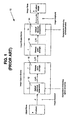
- FIG. 1 illustrates the main elements of a conventional image capture/display device 10 and the optical anomalies present within the corresponding image processing chain that is represented as image (i.e. pixel level) transformations.
- image i.e. pixel level
- Capture/display device 10 contains various elements, including optical elements e.g. lenses, prisms, mirrors, etc.) and non-optical elements (e.g. electronic sensors and display panels) 12 and 14 some or all of which may introduce an optical anomaly into the image processing chain as shown.
- Capture/display device 10 also includes memory (i.e. storage) 16 and 18 as shown.
- Each optical anomaly acts in the spatial space (affecting the shape of the imaged object) and/or in the color space (affecting the brightness/color of the imaged object).
- These effects can be represented as transformations or mappings of (a) pixel positions and (b) pixel colors, that are applied somewhere between the memory plane (space) 16 and 18 and the corresponding object/image plane. Accordingly, these transformations define the optical anomalies. It should be understood that the current representation does not consider differential focus anomalies as differential focus problems cannot be corrected electronically.
- FIG. 1 shows the processing chain where the maps representing the collective effect of all the anomalies on the capture side (defined by subscript c ) by f c and on the display side (defined by subscript d ) by f d .
- the optical anomalies present within capture/display device 10 are represented by these maps.
- the map I associated with storage at the memory plane represents the identity map, which indicates that is there is no change in the image as the memory planes 16 and 18 do not introduce any anomalies.
- optical anomaly is used to refer to any effect that leads to an non-ideal image formation, in particular this includes aberrations and luminance non-uniformity.
- FIG. 2 illustrates how the map f c can be further split into f c s and f c c , where f c s describes spatial anomalies (superscript s ) and f c c describes color anomalies (superscript c ). Since each color component may transform differently, f c s and f c c should be replaced by f cr s , f cg s , f cb s and f cr c , f cg c , f cb c , for the red, green and blue components (second subscripts r , g , b ).
- f c s and f c c will be used when referring to all three component functions together.
- the spatial/color maps representing the anomalies on the display side are denoted by f d s and f d c with their color components f dr s , f dg s , f db s , f dr c , f dg c and f db c .
- the specifics (size, type, etc.) of the memory planes are system dependent and that the memory planes shown represent conceptual domains for the various maps rather than actual hardware implementations of storage.
- the memory plane on the display side is shown in dotted outline to indicate that it need not be present in a specific device, Instead, a captured image may be directly displayed without being stored. If additional processing is conducted in the display part of capture/display device 10 (e.g. frame rate conversion) then some form of physical memory will be required. Furthermore, the memory plane on the capture side does need not be full frame.
- An object O in the object plane is defined by its 2D position vector x (for a point) and its RGB value ( O r ,O g ,O b ).
- the point object is approximated by a pixel. Due to chromatic aberration, the color components of this object will be mapped to different points in the image plane. In general, the single point will be mapped to three points as the three colors are brought to focus to different points (on the same plane).
- the image of the object in the image plane will be described by three position vectors ( x ' r , x ' g , x ' b ) and the corresponding color values ( O ' r , O ' g , O ' b ).
- mappings all spatial maps are represented as vector functions, although to simplify notation the vector arrow has been omitted.
- the corresponding image processing chain is shown in FIG. 2 .
- the notation q (z), for a mapping q and variable z means that q acts to modify z only, changing it to a new value of the same type (i.e. a new position value or a new color value).
- the mapping q can also depend on other variables, however in order to simplify the notation, these are not shown.
- all spatial mappings depend only on spatial variables, whereas the color mappings can depend on both spatial and color variables, as will be further described.
- FIG. 3 illustrates the ideal behaviour of capture/display device 10.
- the correcting maps will try to restore this ideal behavior.
- x ⁇ ⁇ ⁇ k ⁇ x ⁇ , where capture/display device 10 only linearly scales objects in the object plane.
- FIG. 4 illustrates the main elements associated with the electronic correction system 50, made accordance with the present invention.
- Electronic correction system 50 uses image processor 51 to eliminate optical anomalies common to image capture/display devices by introducing an additional 'inverse' transformation in the processing chain discussed above.
- electronic correction system 50 includes optical elements (e.g. lenses, prisms, mirrors, etc.) and non-optical elements (e.g. electronic sensors and panels) 52 and 54 some or all of which may introduce an optical anomaly into the image processing chain as shown, as well as memory plane (i.e. storage plane) 56 and 58 which is assumed not to introduce any anomalies. While both a capture and a display device are shown, it should be understood that the present invention could be easily adapted for use with a capture or display device alone.
- optical elements e.g. lenses, prisms, mirrors, etc.
- non-optical elements e.g. electronic sensors and panels
- memory plane i.e. storage plane
- equations (2) to (7) describe the optical anomalies as transformations in the spatial and color domains.
- Image processor 51 applies arbitrary geometric (spatial) and color transformations to digital images. Spatial transformations are well known and it should be understood that similar transformations can be used to achieve color transformation. Implementation of these spatial transformations can be implemented by image processor 51 using various commercially available image warp circuits (e.g. the sxW1 integrated circuit manufactured by Silicon Optix of San Jose, California) where certain circuits work in the spatial domain and others can also apply color transformations.
- image warp circuits e.g. the sxW1 integrated circuit manufactured by Silicon Optix of San Jose, California
- Image processor 51 processes each color from an image independently, allowing the transformations to be different for the three channels.
- Image processor 51 is placed within the processing chain at the capture-display interface as shown.
- the transformations due to image processor 51 will be denoted by f wr s , f wg s and f wb s (first subscript w ) for the three spatial mappings, and f wr c , f wg c and f wb c for the three-color mappings.
- the processing chain as shown in FIG.
- image processor 51 applies the transformations in equations (26) to (31), the optical anomalies of distortion, color non-convergence (excluding axial chromatic aberration) and luminance (chrominance) non-uniformity will be eliminated.
- Implicit in transformations (26) to (31) is the filtering that accompanies any image warping. After the geometric transformations f wr s , f wg s and f wb s are applied; re-sampling (of all three channels) is needed to generate the new image or pixel data. In image processor 51, these filtering operations often take place before the color transformations f wr c , f wg c and f wb c are applied. The color mappings are then applied to the new filtered pixel data, implying that the anomaly correcting transformations (29) to (31) need to be based on the new image data.
- FIG. 5 illustrates the specific processing sequence that occurs within image processor 51, where a spatial filter 47 performs the filtering operation denoted by F .
- the geometric data received for each output pixel is used by spatial filter 47 to acquire a number of input pixels for transform by FIR filter to an output pixel value.
- a gain and offset stage 49 is utilized to ensure that uniform luminance/chrominance results as previously discussed.
- spatial filter 47 is used to combine F with f cr c - 1 to eliminate the capture side luminosity anomaly.
- the filtering F is implicit in all processing chains or equations that include an image warping circuit. Also implicit is the fact that the color transformations are indirectly linked to the spatial transformations via the filtering.
- the spatial mappings can also directly interact with the color maps. It is contemplated that image processor 51 could be configured to allow for the dynamic modulation of the color map parameters according to the spatial data (e.g. positional/derivative information) being generated. This option is shown in FIG. 5 by the dotted arrow running between the space mapping element and the color-mapping element.
- the generation of the spatial mappings can be performed by an attached processing block or offline (i.e. not within image processor 51), and stored as depicted by geometric transform dataset 57 and luminance transform dataset 59 in FIG. 5 .
- FIG. 6 illustrates another example electronic correction system 100 which uses image processor 101 to implement a further generalization of the transformations (26) to (31) to include an application specific "correction" or warping component (i.e. a component that is independent of the components that correct for the optical defects).
- electronic correction system 100 includes optical elements (e.g. lenses, prisms, mirrors, etc.) and non-optical elements (e.g. electronic sensors and display panels) 102 and 104 some or all of which may introduce an optical anomaly into the image processing chain as shown, as well as memory plane (i.e. storage plane) 106 and 108 which is assumed not to introduce any anomalies.
- optical elements e.g. lenses, prisms, mirrors, etc.
- non-optical elements e.g. electronic sensors and display panels
- memory plane i.e. storage plane
- F an "effective filtering” denotes the filtering accompanying f a s in the absence of any anomalies.
- F plays a role in both eliminating the anomalies and applying the application specific filtering due to f a s .
- mappings f a s and f a c can be different for the three colors, however, for most practical purposes these mappings are the same for all colors. It should be understood that having f a s be different for the three colors is equivalently to 'artificially' introducing lateral chromatic aberration. It should be noted that f a s and f a c do not serve to correct the optical anomalies, and their inputs/outputs are assumed to be anomaly free. Accordingly, the effective processing chain, with the anomalies removed, is shown in FIG. 6 . Once image processor 101 has eliminated the optical anomalies, image processor 101 effectively acts as an application specific image warping circuit. FIG. 7 shows an effective processing chain that resides inside the image processor 101.
- An example of electronic correction system 100 i.e. capture/display device
- capture/display device is one that applies transformations (34) to (39) and that films (captures) a scene and projects (displays) it onto a curved screen.
- f a s and f a c will correct for the distortion (in position and/or color) that arises when projecting onto a curved screen.
- the remaining mapping components will correct for the optical anomalies due to the capture/display optical/electronic components.
- These remaining mapping components are device dependent mappings so that if the screen shape changes, only f a s and f a c change, whereas the device dependent mappings would be unchanged.
- mappings f ci s - 1 , f di s - 1 , f ci c - 1 , f di c - 1 , h c s , h d s , h c c and h d c need only be computed once for a given device configuration.
- One application that might require different f a c mappings for each color is that of color matching.
- the three colors (in each image) in the overlap region need to be adjusted individually to present a seamless transition.
- mappings are an application/device dependent.
- the most general description of a mapping is in terms of a grid dataset.
- a grid dataset gives a representative set of pixels' input/output positions and colors values.
- Various methods can be used to generate a grid dataset.
- a ray-tracing program can be used to determine input and output pixel positions.
- Test patterns can also be run through the system to determine color shifts.
- Data on input and output brightness levels can determine the grid dataset (in color space) that describes the luminance correcting map.
- the grid datasets for the inverse functions in transformations (34) to (39) can be computed by inverting the grid datasets from the 'forward' maps in transformations (2) to (7).
- the conventional understanding relating to spatial transformations can be applied to determine ((42) to ((44).
- the coefficients of the color map ((42) are being fitted in ((43) to ((44).
- the surfaces ((43) to ((44) are determined in exactly the same manner as surface (41); only the meaning of the range is different.
- the color map is taken to be linear; higher order functions may be used though the physical significance of higher order surfaces is not clear.
- Image processor 51 ( FIG. 5 ) and 101 takes ((42) to be linear in O i and ((43) to ((44) to be linear in x and y .
- FIG. 8 illustrates another example electronic correction system 150 which uses image processor 151 to achieve dynamic optical correction and image warping.
- the different transformations which define the dynamic sequence can be computed using a map generator 162 and stored in an external memory 160.
- electronic correction system 150 includes optical elements (e.g. lenses, prisms, etc.) and non-optical elements (e.g. electronic sensors and panels) 152 and 154 some or all of which may introduce an optical anomaly into the image processing chain as shown, as well as memory (i.e. storage plane) 156 and 158 which is assumed not to introduce any anomalies.
- optical elements e.g. lenses, prisms, etc.
- non-optical elements e.g. electronic sensors and panels
- Electronic correction system 150 uses image processor 151 to store different mappings (i.e. more than one set of functions (41) to ((44)). Using this approach, situations where the optical anomalies (and/or application specific warping) change with time (at a reasonable rate) can be addressed. This corresponds to adaptive anomaly correction, where the mappings adapt to the changing anomalies.
- the functions can be pre-computed according to the dynamic changes and then loaded as needed. Dynamic application specific effects can also be included, for example a keystone correction that changes with time.
- the mappings are computed offline, this need not be the case. Given enough computational power, the mappings could be calculated online (i.e. inside an integrated circuit) which will eliminate the memory block required to store the various maps.
- the above electronic solution to optical anomaly correction greatly reduces the cost of a system.
- expensive optical elements can be eliminated or replaced by cheaper components.
- the current circuit can correct distortion, lateral chromatic aberration and luminance/chrominance non-uniformity, as well as apply any application specific image warping.
- a prime market for electronic correction system 150 is in the area of high-resolution pixelated display systems which are used in HDTV's, PC monitors, projection TV's etc.
- FIG. 9 is a flowchart that illustrates the main process steps associated with the electronic correction method 200 of the present invention made accordance with the present invention. As discussed in detail above, electronic correction method 200 eliminates optical anomalies common to image capture/display devices.
- an offline circuit, or possibly image processor 51, 101 and 151 identifies various optical anomalies and collectively represents them as transformations of pixel data.
- the transformations can be in spatial (positional) space and/or color space. As discussed above, the most general way of specifying a transformation is through grid datasets, which give a representative set of pixels' input/output positions and color values.
- the ideal behavior of the processing chain is also identified and represented as grid datasets.
- the anomaly correcting transformations i.e. in the form of grid datasets
- these can be computed by inverting the grid datasets from the previous steps.
- any application specific transformations grid datasets
- the anomaly correcting and application specific transformations, or grid datasets are concatenated into a single dataset. This gives one dataset, for each independent pixel variable, which specifies the complete 'warp' map that is to be applied electronically. There are six independent pixel variables, namely RGB positional values and RGB color values.
- the concatenated grid datasets are converted to a device specific functional format used by commercially available image warp circuits (e.g. the sxW1 integrated circuit manufactured by Silicon Optix of San Jose, California).
- This functional description is capable of representing very general transformations in a manner that is appropriate for real-time, sub-pixel accurate, image processing.
- the pixel data is digitally transformed, according to the pre-computed functional description, via the sxW1 integrated circuit.
- Electronic correction system 50, 100 and 150 and electronic correction method 200 provide efficient and cost-effective real-time electronic correction of aberrations that do not affect image sharpness, namely distortions and color non-convergence (excluding axial chromatic aberration) and luminance (or chrominance) non-uniformity.
- Each of these effects are modelled as transformations in either spatial (positional) space or color space. That is, once an aberration is expressed as a pixel transformation (affecting either pixel positions or pixel color content), it can be eliminated by applying the inverse transformation.
- the same approach also provides for application specific image processing and dynamic anomaly correction.
- Electronic correction method 200 is not restricted to display/projection devices or capture devices, but may be used in conjunction with any image processing chain containing a display and/or capture component. All corrections are represented as grid datasets or functions acting in spatial or color space, which allows different corrections to be concatenated through functional compositions.
Abstract
Description
- This invention relates to electronic correction of optical anomalies and more particularly to electronic correction of distortion, lateral chromatic aberration, luminance non-uniformity,and chrominance non-uniformity, which can be combined with a general image transform (e.g. scaling and geometric transform).
- Conventional image capture or display devices are prone to various forms of optical anomalies. These anomalies are inherent to the non-ideal behavior of the various optical elements and to accuracy and tolerance of assembly. Various components (sensors, displays, lens, prisms, mirrors, light source), optical or otherwise, and their orientation may introduce their own specific optical anomalies, such as distortion, tilt, lateral chromatic aberration, luminance or chrominance non-uniformity. The term optical aberration is generally used to refer to any effect that leads to an non-ideal image formation..
- Optical aberrations include diffraction effects (due to the wave nature of light), chromatic aberrations (caused by optical dispersion, or the differences in refraction in different wavelengths of light), and monochromatic aberrations (of which spherical aberration, coma, and astigmatism are concerned with failures of a point object to form a point image, and field curvature and distortion are concerned with the failure of finite objects perpendicular to the principal axis to form a well-focused plane image). One can also loosely group optical aberrations into two types, ones that affect image quality and ones that affect image shape. The former types degrade the sharpness of an image, that is, the image appears blurred, and/or out of focus, and/or has color fringes. Aberrations in this category include spherical aberrations, astigmatism, coma, field of curvature and axial chromatic aberration. The latter types of aberrations affect the shape of the image that in part may be induced by the former aberration or by the correction and optimization of the former aberration. In this case, points in the object plane are shifted or distorted in comparison with an ideal mapping in the image plane. In an ideal mapping an object in the image plane will appear as it does in the object plane, with possibly a uniform scale change. For example, an image may appear curved near the edges or appear rotated. Aberrations in this second category include distortions (e.g. pincushion/barrel effects) and lateral chromatic aberrations.
- With the exception of chromatic aberrations, all other optical aberrations are present in monochromatic (i.e. single color) light. Chromatic aberration appears when dealing with polychromatic light (many colors). In short, the index of refraction is wavelength dependent, which means that the red, green and blue components bend differently at an optical interface. This leads to axial (longitudinal) and/or lateral chromatic aberration effects. In axial chromatic aberration, the three components are brought to focus on different planes in the image space, which gives a color blurring effect. In other words, axial chromatic aberration arises due to the focal length varying with wavelength (color). In lateral chromatic aberration, color components from a single point are brought to focus to different points on the same image plane. This has the effect of magnifying the three colors differently and can be visually seen as 'color fringing'. Thus lateral chromatic aberration can be seen as an effect due to magnification varying with wavelength. The three colors can also mismatch due to non-optical effects. In a three-color display system, if the displays are not correctly aligned, color defects will be seen. The term color non-convergence is used to refer to color mismatch effects, whether optical (as in chromatic aberrations) or not. Further discussion on optical aberrations can be found in conventional optics textbooks, such as Robert Guenther's Modern Optics, published by John Wiley & Sons, 1990.
- Another important optical anomaly in conventional capture/display devices is luminance non-uniformity. Luminance non-uniformity leads to varying brightness across an image. Common causes include a varying (in brightness) light source, varying optical path across the image plane, non-uniform sensor response and irregularities in panels (e.g. LCD, LCOS, etc.). Both large-scale and small-scale non-uniformities can be present. In a three-color system, brightness variation can be different for each color, leading to chrominance non-uniformity.
- There have been a number of prior art attempts to correct aberrations that affect the shape of the image, without introducing blur, namely correction of distortion, lateral chromatic aberration and luminance or chrominance (brightness) non-uniformity. Generally, such prior art attempts are geared towards one specific type of anomaly.
- For example, lateral chromatic aberration is commonly corrected (or minimized) using special optical elements, often consisting of prism/lens combinations and/or special material coatings such as that disclosed in
U.S. Patent Nos. 4,943,155 to Cross ,5,086,338 to Usui ,5,499,139 to Chen et al. ,6,023,375 to Kreitzer ,6,111,701 to Brown ,6,144, 498 to Bryars et al. , and6,172,815 to Hashizume et al . However, the physical implementation of the solutions disclosed in these references are expensive and bulky. Further, the specialized nature of these designs necessarily restrict them to specific types of applications. Typically, these methods are aimed at display/projection systems or head up/mounted display systems. - A number of electronic solutions have also been presented such as those disclosed in
U.S. Patent Nos. 5,838,396 to Shiota et al. ,5,870,505 to Munib et al. ,6,288,756 to Shiota et al. ,5,200,815 to Tsujihara et al. ,5,369,450 to Haseltine et al ,5,889,625 to Chen et al. , and6,323,934 to Enomoto et al . All of these approaches rely on some type of image "warping". A discussion of image warping can be found in George Wolberg, Digial Image Warping, IEEE Computer Society Press, 1988. - The warping data (i.e. data which describes how the image is to be transformed) may be used to adjust the digital image (e.g. as in
U.S. Patent Nos. 5,369,450 to Haseltine et al. and5,889,625 to Chen et al. ) or to adjust the operation of the electronics that display/project the image (e.g. as inU.S. Patent No. 5,200,815 ). These electronic solutions concentrate on specific anomalies, such as luminance correction (e.g.U.S. Patent Nos. 5,838,396 to Shiota et al. ,5,870,505 to Woeber et al ,6,288,756 to Shiota et al. ), distortion and chromatic aberration (e.g.5,200,815 to Tsujihara et al. ,5,369,450 to Haseltine et al ,5,889,625 to Chen et al. , and6,323,934 to Enomoto et al .) or specific types of systems, such as head-mounted displays. Those solutions that do correct for all three anomalies (e.g.U.S. Patent No. 6,323,934 to Enomoto et al. ) are not real-time in nature. Other limitations of prior art electronic solutions are that they do not allow for application specific "correction" (i.e. correction which does not correspond to an optical anomaly correction) and/or they do not provide for dynamic anomaly correction. For example, it can be desirable in certain video applications to combine anomaly correction (brightness non-uniformity as well as pincushion distortion) with a keystone correction (caused by off-axis projection) and curvature correction for planar/curved surfaces. - The invention provides in one aspect, an electronic correction method for correcting a plurality of optical anomalies associated with the image capture and image display of an optical image processed through optical capture and display components having physical and geometrical characteristics, by compensation of the digital image pixel data associated with the optical image, said method comprising:
- (a) identifying and representing each of the optical anomalies associated with the physical and geometrical characteristics of the optical capture and display components as an optical anomaly grid dataset;
- (b) identifying and representing the ideal behavior of the optical capture and display components as an ideal grid dataset;
- (c) for each optical anomaly grid dataset:
- (i) comparing the optical anomaly grid dataset with the grid dataset and determining an anomaly correcting grid dataset;
- (ii) fitting a two-dimensional surface function to represent the anomaly correcting grid data set;
- (d) concatenating the two-dimensional surface functions of (c) to form a general two-dimensional surface function representing an anomaly correcting transformation for the optical anomalies; and
- (e) applying the anomaly correcting transformation to the digital image pixel data to produce corrected image pixel data which when viewed is free of the optical anomalies.
- The invention provides in another aspect, an electronic correction system for correcting a plurality of optical anomalies associated with the capture and display of an optical image processed through optical capture and display components having a particular geometry, by compensation of the digital image pixel data associated with the optical image, said system comprising an image processor (51) for:
- (a) identifying and representing each of the optical anomalies associated with the physical and geometrical characteristics of the optical capture and display components as an optical anomaly grid dataset;
- (b) identifying and representing the ideal behavior of the optical capture and display components as an ideal grid dataset;
- (c) for each optical anomaly grid dataset:
- (i) comparing the optical anomaly grid dataset with the ideal grid dataset and determining an anomaly correcting grid dataset;
- (ii) fitting a two-dimensional surface function to represent the anomaly correcting grid data set;
- (d) concatenating the two-dimensional surface functions of (c) to form a general two-dimensional surface function representing an anomaly correcting transformation for the optical anomalies; and
- (e) applying the anomaly correcting transformation to the digital image pixel data to produce corrected image pixel data which when viewed is free of the optical anomalies.
- The invention provides in another aspect a computer-readable medium having computer-readable instructions embodied therein for correcting a plurality of optical anomalies associated with the capture and display of an optical image processed through optical capture and display components having a particular geometry, by compensation of the digital image pixel data associated with the optical image, by:
- (a) identifying and representing each of the optical anomalies associated with the physical and geometrical characteristics of the optical capture and display components as an optical anomaly grid dataset;
- (b) identifying and representing the ideal behaviour of the optical capture and display components as an ideal grid dataset;
- (c) for each optical anomaly grid dataset:
- (i) comparing the optical anomaly grid dataset with the ideal grid dataset and determining an anomaly correcting grid dataset;
- (ii) fitting a two-dimensional surface function to represent the anomaly correcting grid data set;
- (d) concatenating the two-dimensional surface functions of (c) to form a general two-dimensional surface function representing an anomaly correcting transformation for the optical anomalies; and
- (e) applying the anomaly correcting transformation to the digital image pixel data to produce corrected image pixel data which when viewed is free of the optical anomalies.
- Further aspects and advantages of the invention will appear from the following description of preferred embodiments, given by way of example only, taken together with the accompanying drawings.
- In the accompanying drawings:
-
FIG. 1 is a schematic diagram illustrating a conventional prior art integrated capture and display device and its corresponding image processing chain; -
FIG. 2 is a schematic diagram illustrating a detailed processing chain and the various transformations that represent the optical defects within the prior art integrated capture and display device ofFIG. 1 ; -
FIG. 3 is a schematic diagram that illustrates an ideal processing chain in the absence of any optical defects; -
FIG. 4 is a schematic diagram of an example of an electronic correction system of the present invention; -
FIG. 5 is a schematic diagram of the correction module of the electronic correction system ofFIG. 4 where the correction module has been adapted to correct for distortion and chrominance non-uniformity; -
FIG. 6 is a schematic diagram of another example of an electronic correction system of the present invention that executes a geometric transform; -
FIG. 7 is a schematic diagram of the correction module of the electronic correction system ofFIG. 6 where the correction module has been adapted to implement an application specific geometric transform; -
FIG. 8 is a schematic diagram of another example of an electronic correction system of the present invention that corrects optical anomalies, executes geometric transforms, and achieves dynamic correction; and -
FIG. 9 is a flowchart illustrating the main steps of an electronic correction method according to the present invention. -
FIG. 1 illustrates the main elements of a conventional image capture/display device 10 and the optical anomalies present within the corresponding image processing chain that is represented as image (i.e. pixel level) transformations. As shown, an object O in the object plane is mapped, via the image processing chain, onto an object O' in the image plane. Capture/display device 10 contains various elements, including optical elements e.g. lenses, prisms, mirrors, etc.) and non-optical elements (e.g. electronic sensors and display panels) 12 and 14 some or all of which may introduce an optical anomaly into the image processing chain as shown. Capture/display device 10 also includes memory (i.e. storage) 16 and 18 as shown. - Each optical anomaly acts in the spatial space (affecting the shape of the imaged object) and/or in the color space (affecting the brightness/color of the imaged object). These effects can be represented as transformations or mappings of (a) pixel positions and (b) pixel colors, that are applied somewhere between the memory plane (space) 16 and 18 and the corresponding object/image plane. Accordingly, these transformations define the optical anomalies. It should be understood that the current representation does not consider differential focus anomalies as differential focus problems cannot be corrected electronically.
-
FIG. 1 shows the processing chain where the maps representing the collective effect of all the anomalies on the capture side (defined by subscript c) by fc and on the display side (defined by subscript d) by fd. The optical anomalies present within capture/display device 10 are represented by these maps. The map I associated with storage at the memory plane represents the identity map, which indicates that is there is no change in the image as the memory planes 16 and 18 do not introduce any anomalies. It should be noted that the term optical anomaly is used to refer to any effect that leads to an non-ideal image formation, in particular this includes aberrations and luminance non-uniformity. -
FIG. 2 illustrates how the map fc can be further split into


- An object O in the object plane is defined by its 2D position vector
x (for a point) and its RGB value (Or,Og,Ob ). In its digital form, the point object is approximated by a pixel. Due to chromatic aberration, the color components of this object will be mapped to different points in the image plane. In general, the single point will be mapped to three points as the three colors are brought to focus to different points (on the same plane). Thus, the image of the object in the image plane will be described by three position vectors (x ' r ,x ' g ,x ' b) and the corresponding color values (O' r ,O' g ,O' b ). It is also useful to introduce the notation (x r ,x g ,x b ) for the spatial coordinates of the three colors in the object space, with the understanding that for a given point we havex =x r , =x g =x b . - Combining everything, the processing of a point object O (or pixel) through capture/
display device 10 in the presence of optical anomalies can be expressed by the following mappings (all spatial maps are represented as vector functions, although to simplify notation the vector arrow has been omitted):


- The corresponding image processing chain is shown in
FIG. 2 . The notation q(z), for a mapping q and variable z , means that q acts to modify z only, changing it to a new value of the same type (i.e. a new position value or a new color value). The mapping q can also depend on other variables, however in order to simplify the notation, these are not shown. For example, z' = q(z,w) is written as z' = q(z). In general, all spatial mappings depend only on spatial variables, whereas the color mappings can depend on both spatial and color variables, as will be further described. -
FIG. 3 illustrates the ideal behaviour of capture/display device 10. To correct the various optical anomalies, we also need to describe the 'ideal' capture/display device in the absence of any anomalies. The correcting maps will try to restore this ideal behavior. In the absence of any lateral chromatic aberration we will have the following relation:
wherex ' represents the common vector for all three colors. Additionally, in the absence of any distortion one expects the following relation:
where capture/display device 10 only linearly scales objects in the object plane. The value "k" represents a spatial scaling constant. Thus zooming operations are not considered as distortions (when such operations are identical for each color). Lastly, for uniform luminance/chrominance one expects the following relation:


where the same change in each color component occurs all across the image (independent ofx ). The "s" and "m" values represent the uniform luminance/ chrominance gain and offset values applied, respectively. The processing of a point object O (or pixel) through capture/display device 10 in the absence of any optical anomalies can be expressed by the following mappings (using h for the ideal mappings):


where


- It should be understood that other forms of ideal behavior can be specified, and that the equations above, namely (9)-(12) are just one example representation.
-
FIG. 4 illustrates the main elements associated with theelectronic correction system 50, made accordance with the present invention.Electronic correction system 50 usesimage processor 51 to eliminate optical anomalies common to image capture/display devices by introducing an additional 'inverse' transformation in the processing chain discussed above. As before,electronic correction system 50 includes optical elements (e.g. lenses, prisms, mirrors, etc.) and non-optical elements (e.g. electronic sensors and panels) 52 and 54 some or all of which may introduce an optical anomaly into the image processing chain as shown, as well as memory plane (i.e. storage plane) 56 and 58 which is assumed not to introduce any anomalies. While both a capture and a display device are shown, it should be understood that the present invention could be easily adapted for use with a capture or display device alone. - As discussed above in respect of
FIG. 2 , equations (2) to (7) describe the optical anomalies as transformations in the spatial and color domains.Image processor 51 applies arbitrary geometric (spatial) and color transformations to digital images. Spatial transformations are well known and it should be understood that similar transformations can be used to achieve color transformation. Implementation of these spatial transformations can be implemented byimage processor 51 using various commercially available image warp circuits (e.g. the sxW1 integrated circuit manufactured by Silicon Optix of San Jose, California) where certain circuits work in the spatial domain and others can also apply color transformations. -
Image processor 51 processes each color from an image independently, allowing the transformations to be different for the three channels.Image processor 51 is placed within the processing chain at the capture-display interface as shown. The transformations due toimage processor 51 will be denoted by


FIG. 4 is now modified to:


- To eliminate the optical anomalies, the transformations utilized within
image processor 51 are chosen such that equations (19) to (25) reduce to (13) to (17). Comparing equations (19) to (25) with equations (13) to (17) gives (it should be understood that multiplication in the relations below implies functional composition):


- The above equations are obtained by appropriately equating (19) to (25) with (13) to (17). For example, to derive (26), set


- When
image processor 51 applies the transformations in equations (26) to (31), the optical anomalies of distortion, color non-convergence (excluding axial chromatic aberration) and luminance (chrominance) non-uniformity will be eliminated. - Implicit in transformations (26) to (31) is the filtering that accompanies any image warping. After the geometric transformations


image processor 51, these filtering operations often take place before the color transformations

-
FIG. 5 illustrates the specific processing sequence that occurs withinimage processor 51, where aspatial filter 47 performs the filtering operation denoted by F . The geometric data received for each output pixel is used byspatial filter 47 to acquire a number of input pixels for transform by FIR filter to an output pixel value. Also, a gain and offsetstage 49 is utilized to ensure that uniform luminance/chrominance results as previously discussed. As a specific example, transformation (29) will correct the luminance non-uniformity if the component mapping


and so forth for the other cases. Herespatial filter 47 is used to combine F with
image processor 51 could be configured to allow for the dynamic modulation of the color map parameters according to the spatial data (e.g. positional/derivative information) being generated. This option is shown inFIG. 5 by the dotted arrow running between the space mapping element and the color-mapping element. The generation of the spatial mappings can be performed by an attached processing block or offline (i.e. not within image processor 51), and stored as depicted bygeometric transform dataset 57 andluminance transform dataset 59 inFIG. 5 . -
FIG. 6 illustrates another exampleelectronic correction system 100 which usesimage processor 101 to implement a further generalization of the transformations (26) to (31) to include an application specific "correction" or warping component (i.e. a component that is independent of the components that correct for the optical defects). As before,electronic correction system 100 includes optical elements (e.g. lenses, prisms, mirrors, etc.) and non-optical elements (e.g. electronic sensors and display panels) 102 and 104 some or all of which may introduce an optical anomaly into the image processing chain as shown, as well as memory plane (i.e. storage plane) 106 and 108 which is assumed not to introduce any anomalies. - Denoting the application specific mappings by


- With an application specific component, equation (33) becomes:

whereF , an "effective filtering", denotes the filtering accompanying

F ), is specified by correctly choosing

- In general the mappings


FIG. 6 . Onceimage processor 101 has eliminated the optical anomalies,image processor 101 effectively acts as an application specific image warping circuit.FIG. 7 shows an effective processing chain that resides inside theimage processor 101. - An example of electronic correction system 100 (i.e. capture/display device) is one that applies transformations (34) to (39) and that films (captures) a scene and projects (displays) it onto a curved screen. In this case


- As previously noted, the method for representation and computation of the various mappings is an application/device dependent. The most general description of a mapping is in terms of a grid dataset. A grid dataset gives a representative set of pixels' input/output positions and colors values. Various methods can be used to generate a grid dataset. For optical elements, a ray-tracing program can be used to determine input and output pixel positions. Test patterns can also be run through the system to determine color shifts. Data on input and output brightness levels can determine the grid dataset (in color space) that describes the luminance correcting map.
- For application specific transforms (keystone, cylinder, sphere, etc), a mathematical model can be used to generate the datasets analytically.. Accordingly, the grid datasets for the inverse functions in transformations (34) to (39) can be computed by inverting the grid datasets from the 'forward' maps in transformations (2) to (7).
- Once the individual datasets (corresponding to the five component functions on the right of (34) to (39)) are determined, these can be concatenated to give one grid dataset for each of the mappings (34) to (39). Concatenation can be done in several ways. One approach is to first fit or interpolate the individual datasets by 2D surfaces, such as splines, etc. These surfaces can then be functionally composed and evaluated in the correct order to obtain the final grid dataset. This process is repeated for each of the mappings (34) to (39). The composition/evaluation operation simply uses the range of one surface as the domain of the next surface, in order. Once we have the final six grid sets, these are then converted to a unifying 2D surface based functional format for representing arbitrary transformations. There are substantial benefits of using this unifying functional format over a (pixel based) grid dataset format. The final result is that (34)-(39) can be expressed as:


- The conventional understanding relating to spatial transformations, namely (41), can be applied to determine ((42) to ((44). Instead of the pixel positions (as in (41)), the coefficients of the color map ((42) are being fitted in ((43) to ((44). The surfaces ((43) to ((44) are determined in exactly the same manner as surface (41); only the meaning of the range is different. In ((42), the color map is taken to be linear; higher order functions may be used though the physical significance of higher order surfaces is not clear. Image processor 51 (
FIG. 5 ) and 101 takes ((42) to be linear in Oi and ((43) to ((44) to be linear in x and y . -
FIG. 8 illustrates another exampleelectronic correction system 150 which usesimage processor 151 to achieve dynamic optical correction and image warping. As shown the different transformations which define the dynamic sequence can be computed using amap generator 162 and stored in anexternal memory 160. As before,electronic correction system 150 includes optical elements (e.g. lenses, prisms, etc.) and non-optical elements (e.g. electronic sensors and panels) 152 and 154 some or all of which may introduce an optical anomaly into the image processing chain as shown, as well as memory (i.e. storage plane) 156 and 158 which is assumed not to introduce any anomalies. -
Electronic correction system 150 usesimage processor 151 to store different mappings (i.e. more than one set of functions (41) to ((44)). Using this approach, situations where the optical anomalies (and/or application specific warping) change with time (at a reasonable rate) can be addressed. This corresponds to adaptive anomaly correction, where the mappings adapt to the changing anomalies. The functions can be pre-computed according to the dynamic changes and then loaded as needed. Dynamic application specific effects can also be included, for example a keystone correction that changes with time. Although it has been assumed that the mappings are computed offline, this need not be the case. Given enough computational power, the mappings could be calculated online (i.e. inside an integrated circuit) which will eliminate the memory block required to store the various maps. - The functions discussed above (41) to ((44) can be stored in
image processor - The above electronic solution to optical anomaly correction greatly reduces the cost of a system. In particular, expensive optical elements can be eliminated or replaced by cheaper components. The current circuit can correct distortion, lateral chromatic aberration and luminance/chrominance non-uniformity, as well as apply any application specific image warping. A prime market for
electronic correction system 150, is in the area of high-resolution pixelated display systems which are used in HDTV's, PC monitors, projection TV's etc. -
FIG. 9 is a flowchart that illustrates the main process steps associated with theelectronic correction method 200 of the present invention made accordance with the present invention. As discussed in detail above,electronic correction method 200 eliminates optical anomalies common to image capture/display devices. - At step (202) an offline circuit, or possibly image
processor - At step (206), the anomaly correcting transformations (i.e. in the form of grid datasets) is computed. These can be computed by inverting the grid datasets from the previous steps. At step (208), any application specific transformations (grid datasets) are computed. At step (210), the anomaly correcting and application specific transformations, or grid datasets, are concatenated into a single dataset. This gives one dataset, for each independent pixel variable, which specifies the complete 'warp' map that is to be applied electronically. There are six independent pixel variables, namely RGB positional values and RGB color values.
- At step (212), the concatenated grid datasets are converted to a device specific functional format used by commercially available image warp circuits (e.g. the sxW1 integrated circuit manufactured by Silicon Optix of San Jose, California). This functional description is capable of representing very general transformations in a manner that is appropriate for real-time, sub-pixel accurate, image processing. Finally, at step (214), the pixel data is digitally transformed, according to the pre-computed functional description, via the sxW1 integrated circuit. As a result, the final image, having gone through the capture/warping/display processing chain, is free of any anomalies and exhibits only the application specific image warping.
-
Electronic correction system electronic correction method 200 provide efficient and cost-effective real-time electronic correction of aberrations that do not affect image sharpness, namely distortions and color non-convergence (excluding axial chromatic aberration) and luminance (or chrominance) non-uniformity. Each of these effects are modelled as transformations in either spatial (positional) space or color space. That is, once an aberration is expressed as a pixel transformation (affecting either pixel positions or pixel color content), it can be eliminated by applying the inverse transformation. The same approach also provides for application specific image processing and dynamic anomaly correction.Electronic correction method 200 is not restricted to display/projection devices or capture devices, but may be used in conjunction with any image processing chain containing a display and/or capture component. All corrections are represented as grid datasets or functions acting in spatial or color space, which allows different corrections to be concatenated through functional compositions. - As will be apparent to those skilled in the art, various modifications and adaptations of the structure described above are possible without departing from the present invention, the scope of which is defined in the appended claims.
Claims (27)
- An electronic correction method for correcting a plurality of optical anomalies associated with the image capture and image display of an optical image processed through optical capture and display components having physical and geometrical characteristics, by compensation of the digital image pixel data associated with the optical image, said method comprising:(a) identifying and representing each of the optical anomalies associated with the physical and geometrical characteristics of the optical capture and display components as an optical anomaly grid dataset;(b) identifying and representing the ideal behavior of the optical capture and display components as an ideal grid dataset;(c) for each optical anomaly grid dataset:(i) comparing the optical anomaly grid dataset with the ideal grid dataset and determining an anomaly correcting grid dataset;(ii) fitting a two-dimensional surface function to represent the anomaly correcting grid data set;(d) concatenating the two-dimensional surface functions of (c) to form a general two-dimensional surface function representing an anomaly correcting transformation for the optical anomalies; and(e) applying the anomaly correcting transformation to the digital image pixel data to produce corrected image pixel data which when viewed is free of the optical anomalies.
- The method of claim 1, wherein said optical anomalies are selected from the group consisting of: distortions, color non-convergence, luminance non-uniformity, and chrominance non-uniformity.
- The method of claim 1, further comprising computing an application specific transformation which represents image scaling and geometric transformations selected from the group consisting of spherical, cylindrical, and keystone transformations, and concatenating the application specific transformation with the anomaly correcting transformation from (d) and where (e) consists of applying the concatenation of the application specific transformation with the anomaly correcting transformation to the digital pixel image data.
- The method of claim 1, wherein the anomaly correcting transformation is converted to a device specific functional representation.
- The method of claim 1, further comprising storing a sequence of transformations to achieve dynamic anomaly correction.
- The method of claim 1, wherein the anomaly correcting transformation is defined in at least one of position space and color space.
- The method of claim 1, wherein the anomaly correcting transformation defines a set of correcting geometric transformations and a set of correcting color transformations.
- The method of claim 7, wherein (e) comprises(i) applying the set of correcting geometric transformations;(ii) applying a set of filtering operations; and(iii) applying the set of correcting color transformations.
- The method of claim 1, wherein the digital pixel image data is associated with at least one of a capture device and a display device.
- An electronic correction system for correcting a plurality of optical anomalies associated with the capture and display of an optical image processed through optical capture and display components having a particular geometry, by compensation of the digital image pixel data associated with the optical image, said system comprising an image processor for:(a) identifying and representing each of the optical anomalies associated with the physical and geometrical characteristics of the optical capture and display components as an optical anomaly grid dataset;(b) identifying and representing the ideal behavior of the optical capture and display components as an ideal grid dataset;(c) for each optical anomaly grid dataset:(i) comparing the optical anomaly grid dataset with the ideal grid dataset and determining an anomaly correcting grid dataset;(ii) fitting a two-dimensional surface function to represent the anomaly correcting grid data set;(d) concatenating the two-dimensional surface functions of (c) to form a general two-dimensional surface function representing an anomaly correcting transformation for the optical anomalies; and(e) applying the anomaly correcting transformation to the digital image pixel data to produce corrected image pixel data which when viewed is free of the optical anomalies.
- The system of claim 10, wherein said optical anomalies are selected from the group consisting of: distortions, color non-convergence, luminance non-uniformity and chrominance non-uniformity.
- The system of claim 10, further comprising an application module for computing an application specific transformation which represents image scaling and geometric transformations selected from the group consisting of spherical, cylindrical, and keystone transformations, and concatenating the application specific transformation with the anomaly correcting transformation from (d) and where (e) consists of applying the concatenation of the application specific transformation with the anomaly correcting transformation to the digital pixel image data.
- The system of claim 10, wherein the image processor is further adapted to convert the anomaly correcting transformation to a device specific functional representation.
- The system of claim 10, wherein the image processor is further adapted to store a sequence of transformations to achieve dynamic anomaly correction.
- The system of claim 10, wherein the optical anomaly grid is defined in at least one of position space and color space.
- The system of claim 10, wherein the anomaly correcting transformation defines a set of correcting geometric transformations and a set of correcting color transformations.
- The system of claim 16, wherein the image processor is further adapted to:(i) apply the set of correcting geometric transformations;(ii) apply a set of filtering operations; and(iii) apply the set of correcting color transformations.
- The system of claim 10, further comprising an image display device coupled to the image processor for displaying said corrected image pixel data.
- The system of claim 10, further comprising an image capture device coupled to the image processor for capturing said digital image pixel data.
- A computer-readable medium having computer-readable instructions embodied therein for correcting a plurality of optical anomalies associated with the capture and display of an optical image processed through optical capture and display components having a particular geometry, by compensation of the digital image pixel data associated with the optical image, by:(a) identifying and representing each of the optical anomalies associated with the physical and geometrical characteristics of the optical capture and display components as an optical anomaly grid dataset;(b) identifying and representing the ideal behavior of the optical capture and display components as an ideal grid dataset;(c) for each optical anomaly grid dataset:(i) comparing the optical anomaly grid dataset with the ideal grid dataset and determining an anomaly correcting grid dataset;(ii) fitting a two-dimensional surface function to represent the anomaly correcting grid data set;(d) concatenating the two-dimensional surface functions of (c) to form a general two-dimensional surface function representing an anomaly correcting transformation for the optical anomalies; and(e) applying the anomaly correcting transformation to the digital image pixel data to produce corrected image pixel data which when viewed is free of the optical anomalies.
- The computer-readable medium of claim 20, wherein said optical anomalies are selected from the group consisting of: distortions, color non-convergence, luminance non-uniformity, and chrominance non-uniformity.
- The computer-readable medium of claim 20, wherein an application specific transformation is computed that represents image scaling and geometric transformations selected from the group consisting of spherical, cylindrical, and keystone transformations, and concatenating the application specific transformation with the anomaly correcting transformation from (d) and where (e) consists of applying the concatenation of the application specific transformation with the anomaly correcting transformation to the digital pixel image data.
- The computer-readable medium of claim 20, wherein the anomaly correcting transformation is converted to a device specific functional representation.
- The computer-readable medium of claim 20, wherein a sequence of transformations are stored to achieve dynamic anomaly correction.
- The computer-readable medium of claim 20, wherein the anomaly correcting transformation is defined in at least one of position space and color space.
- The computer-readable medium of claim 20, wherein the anomaly correcting transformation defines a set of correcting geometric transformations and a set of correcting color transformations.
- The computer-readable medium of claim 26, wherein (e) comprises(i) applying the set of correcting geometric transformations;(ii) applying a set of filtering operations; and(iii) applying the set of correcting color transformations.
Applications Claiming Priority (3)
| Application Number | Priority Date | Filing Date | Title |
|---|---|---|---|
| US38759602P | 2002-06-12 | 2002-06-12 | |
| US387596P | 2002-06-12 | ||
| PCT/CA2003/000888 WO2003107274A2 (en) | 2002-06-12 | 2003-06-12 | System and method for electronic correction of optical anomalies |
Publications (2)
| Publication Number | Publication Date |
|---|---|
| EP1512123A2 EP1512123A2 (en) | 2005-03-09 |
| EP1512123B1 true EP1512123B1 (en) | 2009-10-07 |
Family
ID=29736337
Family Applications (1)
| Application Number | Title | Priority Date | Filing Date |
|---|---|---|---|
| EP03759800A Expired - Lifetime EP1512123B1 (en) | 2002-06-12 | 2003-06-12 | System and method for electronic correction of optical anomalies |
Country Status (9)
| Country | Link |
|---|---|
| US (1) | US7474799B2 (en) |
| EP (1) | EP1512123B1 (en) |
| JP (1) | JP2005535010A (en) |
| KR (1) | KR100973855B1 (en) |
| CN (1) | CN100365658C (en) |
| AT (1) | ATE445203T1 (en) |
| AU (1) | AU2003232561A1 (en) |
| DE (1) | DE60329593D1 (en) |
| WO (1) | WO2003107274A2 (en) |
Families Citing this family (34)
| Publication number | Priority date | Publication date | Assignee | Title |
|---|---|---|---|---|
| US6751362B2 (en) * | 2001-01-11 | 2004-06-15 | Micron Technology, Inc. | Pixel resampling system and method for text |
| US6963348B2 (en) * | 2002-05-31 | 2005-11-08 | Nvidia Corporation | Method and apparatus for display image adjustment |
| US7221793B2 (en) * | 2003-05-27 | 2007-05-22 | Hewlett-Packard Development Company, L.P. | Systems and methods for providing spatially-varied demosaicing |
| WO2006022630A1 (en) * | 2004-07-26 | 2006-03-02 | Silicon Optix, Inc. | Panoramic vision system and method |
| US20060045383A1 (en) * | 2004-08-31 | 2006-03-02 | Picciotto Carl E | Displacement estimation system and method |
| EP1800245B1 (en) * | 2004-09-09 | 2012-01-04 | Silicon Optix Inc. | System and method for representing a general two dimensional spatial transformation |
| US7653447B2 (en) * | 2004-12-30 | 2010-01-26 | Mondo Systems, Inc. | Integrated audio video signal processing system using centralized processing of signals |
| US8015590B2 (en) * | 2004-12-30 | 2011-09-06 | Mondo Systems, Inc. | Integrated multimedia signal processing system using centralized processing of signals |
| US7825986B2 (en) | 2004-12-30 | 2010-11-02 | Mondo Systems, Inc. | Integrated multimedia signal processing system using centralized processing of signals and other peripheral device |
| US8880205B2 (en) | 2004-12-30 | 2014-11-04 | Mondo Systems, Inc. | Integrated multimedia signal processing system using centralized processing of signals |
| US7570810B2 (en) * | 2005-02-24 | 2009-08-04 | Seiko Epson Corporation | Method and apparatus applying digital image filtering to color filter array data |
| US9101279B2 (en) | 2006-02-15 | 2015-08-11 | Virtual Video Reality By Ritchey, Llc | Mobile user borne brain activity data and surrounding environment data correlation system |
| JP5074777B2 (en) | 2006-05-22 | 2012-11-14 | キヤノン株式会社 | Display device with imaging function, image processing device, image processing method, and image display system |
| US20080088527A1 (en) * | 2006-10-17 | 2008-04-17 | Keitaro Fujimori | Heads Up Display System |
| WO2008077132A1 (en) | 2006-12-19 | 2008-06-26 | California Institute Of Technology | Imaging model and apparatus |
| JP2010530087A (en) | 2006-12-19 | 2010-09-02 | 創太 清水 | Image processor |
| US8442316B2 (en) * | 2007-01-05 | 2013-05-14 | Geo Semiconductor Inc. | System and method for improving color and brightness uniformity of backlit LCD displays |
| US8055070B2 (en) * | 2007-01-05 | 2011-11-08 | Geo Semiconductor Inc. | Color and geometry distortion correction system and method |
| JP4827193B2 (en) | 2007-03-23 | 2011-11-30 | オリンパスイメージング株式会社 | Electronic imaging device |
| US8325282B2 (en) * | 2008-04-08 | 2012-12-04 | Mitsubishi Electric Visual Solutions America, Inc. | Television automatic geometry adjustment system |
| US8328365B2 (en) | 2009-04-30 | 2012-12-11 | Hewlett-Packard Development Company, L.P. | Mesh for mapping domains based on regularized fiducial marks |
| DE102010028894B4 (en) | 2009-05-13 | 2018-05-24 | Koh Young Technology Inc. | Method for measuring a measurement object |
| DE102010064640B3 (en) * | 2009-05-13 | 2018-05-09 | Koh Young Technology Inc. | Method for measuring a measurement target |
| CN102550126B (en) * | 2009-10-15 | 2015-09-02 | 株式会社日本有机雷特显示器 | The manufacture method of display device, display device and display device |
| TWI423659B (en) * | 2010-11-09 | 2014-01-11 | Avisonic Technology Corp | Image corretion method and related image corretion system thereof |
| US8854401B2 (en) | 2010-12-28 | 2014-10-07 | Apple Inc. | System and method to improve image edge discoloration |
| US8867831B2 (en) * | 2012-05-09 | 2014-10-21 | University Of Southern California | Image enhancement using modulation strength map and modulation kernel |
| US9251572B2 (en) * | 2013-07-26 | 2016-02-02 | Qualcomm Incorporated | System and method of correcting image artifacts |
| US10438331B2 (en) * | 2014-06-26 | 2019-10-08 | Intel Corporation | Distortion meshes against chromatic aberrations |
| TW201822709A (en) * | 2016-12-30 | 2018-07-01 | 曦威科技股份有限公司 | Real-time heart rate detection method and real-time heart rate detection system therefor |
| US11275920B1 (en) | 2017-09-27 | 2022-03-15 | Apple Inc. | Elongated fingerprint sensor |
| US11227558B1 (en) | 2018-09-07 | 2022-01-18 | Apple Inc. | Subpixel layout compensation to correct color fringing on an electronic display |
| US11189248B1 (en) | 2020-05-06 | 2021-11-30 | Apple Inc. | Systems and methods for switching vision correction graphical outputs on a display of an electronic device |
| US11783629B2 (en) | 2021-03-02 | 2023-10-10 | Apple Inc. | Handheld electronic device |
Family Cites Families (32)
| Publication number | Priority date | Publication date | Assignee | Title |
|---|---|---|---|---|
| US4943155A (en) | 1987-12-22 | 1990-07-24 | Hughes Aircraft Company | Color projection system with a color correction wedge |
| US5086338A (en) | 1988-11-21 | 1992-02-04 | Canon Kabushiki Kaisha | Color television camera optical system adjusting for chromatic aberration |
| US5055922A (en) | 1990-03-07 | 1991-10-08 | U.S. Precision Lens Incorporated | Color tv projection lens system |
| FR2660090B1 (en) * | 1990-03-23 | 1994-07-29 | Thomson Csf | DEVICE FOR VIEWING BY PROJECTION WITH A FEEDBACK LOOP FOR CORRECTING ALL OF THE DEFECTS IN THE PROJECTED IMAGE. |
| JP2653899B2 (en) | 1990-06-07 | 1997-09-17 | 松下電器産業株式会社 | Image correction device |
| US5369450A (en) | 1993-06-01 | 1994-11-29 | The Walt Disney Company | Electronic and computational correction of chromatic aberration associated with an optical system used to view a color video display |
| US6012375A (en) | 1993-07-06 | 2000-01-11 | Eckstein; Donald B. | Aircraft infrared guided defense missile system |
| US5499139A (en) | 1993-10-01 | 1996-03-12 | Hughes Aircraft Company | Ultra-wide field of view, broad spectral band helmet visor display optical system |
| JPH0888860A (en) * | 1994-09-19 | 1996-04-02 | Mitsubishi Electric Corp | Automatic image distortion correction device |
| CN1070013C (en) | 1994-12-14 | 2001-08-22 | 松下电器产业株式会社 | Projection type image display apparatus with circuit for correcting luminance nonuniformity |
| US5870505A (en) | 1996-03-14 | 1999-02-09 | Polaroid Corporation | Method and apparatus for pixel level luminance adjustment |
| JP3309738B2 (en) | 1996-11-01 | 2002-07-29 | 松下電器産業株式会社 | Image display device |
| US6249315B1 (en) * | 1997-03-24 | 2001-06-19 | Jack M. Holm | Strategy for pictorial digital image processing |
| US5889625A (en) * | 1997-05-21 | 1999-03-30 | Raytheon Company | Chromatic aberration correction for display systems |
| JP3575234B2 (en) | 1997-07-15 | 2004-10-13 | セイコーエプソン株式会社 | Dichroic prism and projection display |
| DE19855885A1 (en) | 1997-12-04 | 1999-08-05 | Fuji Photo Film Co Ltd | Image processing method for digital photographic copier providing photographic prints |
| US6069982A (en) * | 1997-12-23 | 2000-05-30 | Polaroid Corporation | Estimation of frequency dependence and grey-level dependence of noise in an image |
| US6144498A (en) | 1998-06-11 | 2000-11-07 | Optical Coating Laboratory, Inc. | Color separation prism assembly and method for making same |
| US6456339B1 (en) * | 1998-07-31 | 2002-09-24 | Massachusetts Institute Of Technology | Super-resolution display |
| JP3395832B2 (en) * | 1998-08-28 | 2003-04-14 | ソニー株式会社 | Image display correction system, image display correction apparatus and method, and image display apparatus and method |
| US6418242B1 (en) * | 1998-11-18 | 2002-07-09 | Tektronix, Inc. | Efficient detection of error blocks in a DCT-based compressed video sequence |
| KR100366643B1 (en) * | 1998-11-25 | 2003-02-19 | 삼성전자 주식회사 | Method and apparatus for de-blocking |
| US6349146B2 (en) * | 1998-12-22 | 2002-02-19 | Xerox Corporation | Device-biased color converting apparatus and method |
| US6459818B1 (en) * | 1999-03-01 | 2002-10-01 | University Of Rochester | System for recovery of degraded images |
| US6111701A (en) | 1999-07-14 | 2000-08-29 | Rockwell Collins, Inc. | Chromatic aberration corrected multi-color head-up display system |
| KR100414083B1 (en) * | 1999-12-18 | 2004-01-07 | 엘지전자 주식회사 | Method for compensating image distortion and image displaying apparatus using the same |
| US6816625B2 (en) * | 2000-08-16 | 2004-11-09 | Lewis Jr Clarence A | Distortion free image capture system and method |
| JP3497805B2 (en) * | 2000-08-29 | 2004-02-16 | オリンパス株式会社 | Image projection display device |
| US6963348B2 (en) * | 2002-05-31 | 2005-11-08 | Nvidia Corporation | Method and apparatus for display image adjustment |
| KR100571219B1 (en) | 2003-01-08 | 2006-04-13 | 엘지전자 주식회사 | Digital convergence device based on 3-d virtual screen of video display system |
| KR100525425B1 (en) | 2003-02-04 | 2005-11-02 | 엘지전자 주식회사 | Image warping method and apparatus |
| JP4600209B2 (en) * | 2005-08-18 | 2010-12-15 | ソニー株式会社 | Image processing method, image processing apparatus, program, and recording medium |
-
2003
- 2003-06-12 US US10/461,320 patent/US7474799B2/en active Active
- 2003-06-12 DE DE60329593T patent/DE60329593D1/en not_active Expired - Lifetime
- 2003-06-12 JP JP2004514012A patent/JP2005535010A/en active Pending
- 2003-06-12 AT AT03759800T patent/ATE445203T1/en not_active IP Right Cessation
- 2003-06-12 CN CNB038136007A patent/CN100365658C/en not_active Expired - Lifetime
- 2003-06-12 AU AU2003232561A patent/AU2003232561A1/en not_active Abandoned
- 2003-06-12 WO PCT/CA2003/000888 patent/WO2003107274A2/en active Application Filing
- 2003-06-12 KR KR1020047020010A patent/KR100973855B1/en active IP Right Grant
- 2003-06-12 EP EP03759800A patent/EP1512123B1/en not_active Expired - Lifetime
Also Published As
| Publication number | Publication date |
|---|---|
| ATE445203T1 (en) | 2009-10-15 |
| US20040076336A1 (en) | 2004-04-22 |
| CN1659592A (en) | 2005-08-24 |
| WO2003107274A2 (en) | 2003-12-24 |
| JP2005535010A (en) | 2005-11-17 |
| KR100973855B1 (en) | 2010-08-03 |
| US7474799B2 (en) | 2009-01-06 |
| WO2003107274A3 (en) | 2004-07-29 |
| AU2003232561A1 (en) | 2003-12-31 |
| DE60329593D1 (en) | 2009-11-19 |
| EP1512123A2 (en) | 2005-03-09 |
| CN100365658C (en) | 2008-01-30 |
| KR20060041142A (en) | 2006-05-11 |
| AU2003232561A8 (en) | 2003-12-31 |
Similar Documents
| Publication | Publication Date | Title |
|---|---|---|
| EP1512123B1 (en) | System and method for electronic correction of optical anomalies | |
| TWI459820B (en) | Color and geometry distortion correction system and method | |
| US8116008B2 (en) | System and method for lens performance optimization using electronic aberration correction | |
| US8406562B2 (en) | System and method for automated calibration and correction of display geometry and color | |
| US7356198B2 (en) | Method and system for calculating a transformed image from a digital image | |
| EP1395865A2 (en) | System and method for correcting keystone distortion | |
| US20050007477A1 (en) | Correction of optical distortion by image processing | |
| EP2362345B1 (en) | Method and apparatus for high-speed and low-complexity piecewise geometric transformation of signals | |
| US20130050544A1 (en) | Image processing apparatus, image capture apparatus, and image processing method | |
| JP2011211426A (en) | Image processing apparatus and method of controlling the same | |
| JPH10322711A (en) | Correction system of spatial non-uniformity for color sensor | |
| JP5479187B2 (en) | Image processing apparatus and imaging apparatus using the same | |
| EP2205002A1 (en) | Spectral characteristic correction device and spectral characteristic correction method | |
| JP2024024012A (en) | Learning data generation method, learning method, learning data production device, learning device, and program | |
| Petrov et al. | Color correction with 3D lookup tables in diffractive optical imaging systems | |
| JP5055588B2 (en) | Image processing apparatus and image processing method | |
| JP7414745B2 (en) | Learning data production method, learning method, learning data production device, learning device, and program | |
| CN115205731A (en) | Video noise reduction device and method and terminal | |
| JP5047700B2 (en) | Image display apparatus, image processing method, and program | |
| US7403207B1 (en) | Intensity weighting for sub-pixel positioning | |
| JPS59109970A (en) | Device for correcting distortion | |
| JPH0737079A (en) | Method and device for correcting picture distortion | |
| Martin | High-resolution color ccd camera | |
| JP2021170197A (en) | Image processing method, image processing device, image processing program, and production method for learned model | |
| Klein | Compensation of Geometric Distortions in Multispectral Imaging |
Legal Events
| Date | Code | Title | Description |
|---|---|---|---|
| PUAI | Public reference made under article 153(3) epc to a published international application that has entered the european phase |
Free format text: ORIGINAL CODE: 0009012 |
|
| 17P | Request for examination filed |
Effective date: 20041213 |
|
| AK | Designated contracting states |
Kind code of ref document: A2 Designated state(s): AT BE BG CH CY CZ DE DK EE ES FI FR GB GR HU IE IT LI LU MC NL PT RO SE SI SK TR |
|
| AX | Request for extension of the european patent |
Extension state: AL LT LV MK |
|
| DAX | Request for extension of the european patent (deleted) | ||
| GRAP | Despatch of communication of intention to grant a patent |
Free format text: ORIGINAL CODE: EPIDOSNIGR1 |
|
| GRAS | Grant fee paid |
Free format text: ORIGINAL CODE: EPIDOSNIGR3 |
|
| GRAA | (expected) grant |
Free format text: ORIGINAL CODE: 0009210 |
|
| AK | Designated contracting states |
Kind code of ref document: B1 Designated state(s): AT BE BG CH CY CZ DE DK EE ES FI FR GB GR HU IE IT LI LU MC NL PT RO SE SI SK TR |
|
| REG | Reference to a national code |
Ref country code: GB Ref legal event code: FG4D |
|
| REG | Reference to a national code |
Ref country code: CH Ref legal event code: EP |
|
| REG | Reference to a national code |
Ref country code: IE Ref legal event code: FG4D |
|
| REF | Corresponds to: |
Ref document number: 60329593 Country of ref document: DE Date of ref document: 20091119 Kind code of ref document: P |
|
| PG25 | Lapsed in a contracting state [announced via postgrant information from national office to epo] |
Ref country code: SI Free format text: LAPSE BECAUSE OF FAILURE TO SUBMIT A TRANSLATION OF THE DESCRIPTION OR TO PAY THE FEE WITHIN THE PRESCRIBED TIME-LIMIT Effective date: 20091007 |
|
| NLV1 | Nl: lapsed or annulled due to failure to fulfill the requirements of art. 29p and 29m of the patents act | ||
| PG25 | Lapsed in a contracting state [announced via postgrant information from national office to epo] |
Ref country code: SE Free format text: LAPSE BECAUSE OF FAILURE TO SUBMIT A TRANSLATION OF THE DESCRIPTION OR TO PAY THE FEE WITHIN THE PRESCRIBED TIME-LIMIT Effective date: 20091007 Ref country code: ES Free format text: LAPSE BECAUSE OF FAILURE TO SUBMIT A TRANSLATION OF THE DESCRIPTION OR TO PAY THE FEE WITHIN THE PRESCRIBED TIME-LIMIT Effective date: 20100118 Ref country code: FI Free format text: LAPSE BECAUSE OF FAILURE TO SUBMIT A TRANSLATION OF THE DESCRIPTION OR TO PAY THE FEE WITHIN THE PRESCRIBED TIME-LIMIT Effective date: 20091007 Ref country code: PT Free format text: LAPSE BECAUSE OF FAILURE TO SUBMIT A TRANSLATION OF THE DESCRIPTION OR TO PAY THE FEE WITHIN THE PRESCRIBED TIME-LIMIT Effective date: 20100208 |
|
| PG25 | Lapsed in a contracting state [announced via postgrant information from national office to epo] |
Ref country code: BE Free format text: LAPSE BECAUSE OF FAILURE TO SUBMIT A TRANSLATION OF THE DESCRIPTION OR TO PAY THE FEE WITHIN THE PRESCRIBED TIME-LIMIT Effective date: 20091007 Ref country code: AT Free format text: LAPSE BECAUSE OF FAILURE TO SUBMIT A TRANSLATION OF THE DESCRIPTION OR TO PAY THE FEE WITHIN THE PRESCRIBED TIME-LIMIT Effective date: 20091007 |
|
| PG25 | Lapsed in a contracting state [announced via postgrant information from national office to epo] |
Ref country code: NL Free format text: LAPSE BECAUSE OF FAILURE TO SUBMIT A TRANSLATION OF THE DESCRIPTION OR TO PAY THE FEE WITHIN THE PRESCRIBED TIME-LIMIT Effective date: 20091007 Ref country code: DK Free format text: LAPSE BECAUSE OF FAILURE TO SUBMIT A TRANSLATION OF THE DESCRIPTION OR TO PAY THE FEE WITHIN THE PRESCRIBED TIME-LIMIT Effective date: 20091007 Ref country code: RO Free format text: LAPSE BECAUSE OF FAILURE TO SUBMIT A TRANSLATION OF THE DESCRIPTION OR TO PAY THE FEE WITHIN THE PRESCRIBED TIME-LIMIT Effective date: 20091007 Ref country code: BG Free format text: LAPSE BECAUSE OF FAILURE TO SUBMIT A TRANSLATION OF THE DESCRIPTION OR TO PAY THE FEE WITHIN THE PRESCRIBED TIME-LIMIT Effective date: 20100107 Ref country code: EE Free format text: LAPSE BECAUSE OF FAILURE TO SUBMIT A TRANSLATION OF THE DESCRIPTION OR TO PAY THE FEE WITHIN THE PRESCRIBED TIME-LIMIT Effective date: 20091007 |
|
| PLBE | No opposition filed within time limit |
Free format text: ORIGINAL CODE: 0009261 |
|
| STAA | Information on the status of an ep patent application or granted ep patent |
Free format text: STATUS: NO OPPOSITION FILED WITHIN TIME LIMIT |
|
| PG25 | Lapsed in a contracting state [announced via postgrant information from national office to epo] |
Ref country code: SK Free format text: LAPSE BECAUSE OF FAILURE TO SUBMIT A TRANSLATION OF THE DESCRIPTION OR TO PAY THE FEE WITHIN THE PRESCRIBED TIME-LIMIT Effective date: 20091007 Ref country code: CZ Free format text: LAPSE BECAUSE OF FAILURE TO SUBMIT A TRANSLATION OF THE DESCRIPTION OR TO PAY THE FEE WITHIN THE PRESCRIBED TIME-LIMIT Effective date: 20091007 |
|
| 26N | No opposition filed |
Effective date: 20100708 |
|
| PG25 | Lapsed in a contracting state [announced via postgrant information from national office to epo] |
Ref country code: GR Free format text: LAPSE BECAUSE OF FAILURE TO SUBMIT A TRANSLATION OF THE DESCRIPTION OR TO PAY THE FEE WITHIN THE PRESCRIBED TIME-LIMIT Effective date: 20100108 |
|
| PG25 | Lapsed in a contracting state [announced via postgrant information from national office to epo] |
Ref country code: MC Free format text: LAPSE BECAUSE OF NON-PAYMENT OF DUE FEES Effective date: 20100630 |
|
| REG | Reference to a national code |
Ref country code: CH Ref legal event code: PL |
|
| REG | Reference to a national code |
Ref country code: FR Ref legal event code: ST Effective date: 20110228 |
|
| PG25 | Lapsed in a contracting state [announced via postgrant information from national office to epo] |
Ref country code: IT Free format text: LAPSE BECAUSE OF FAILURE TO SUBMIT A TRANSLATION OF THE DESCRIPTION OR TO PAY THE FEE WITHIN THE PRESCRIBED TIME-LIMIT Effective date: 20091007 |
|
| PG25 | Lapsed in a contracting state [announced via postgrant information from national office to epo] |
Ref country code: CH Free format text: LAPSE BECAUSE OF NON-PAYMENT OF DUE FEES Effective date: 20100630 Ref country code: LI Free format text: LAPSE BECAUSE OF NON-PAYMENT OF DUE FEES Effective date: 20100630 Ref country code: IE Free format text: LAPSE BECAUSE OF NON-PAYMENT OF DUE FEES Effective date: 20100612 |
|
| PG25 | Lapsed in a contracting state [announced via postgrant information from national office to epo] |
Ref country code: FR Free format text: LAPSE BECAUSE OF NON-PAYMENT OF DUE FEES Effective date: 20100630 |
|
| PG25 | Lapsed in a contracting state [announced via postgrant information from national office to epo] |
Ref country code: CY Free format text: LAPSE BECAUSE OF FAILURE TO SUBMIT A TRANSLATION OF THE DESCRIPTION OR TO PAY THE FEE WITHIN THE PRESCRIBED TIME-LIMIT Effective date: 20091007 |
|
| PG25 | Lapsed in a contracting state [announced via postgrant information from national office to epo] |
Ref country code: HU Free format text: LAPSE BECAUSE OF FAILURE TO SUBMIT A TRANSLATION OF THE DESCRIPTION OR TO PAY THE FEE WITHIN THE PRESCRIBED TIME-LIMIT Effective date: 20100408 Ref country code: LU Free format text: LAPSE BECAUSE OF NON-PAYMENT OF DUE FEES Effective date: 20100612 |
|
| PG25 | Lapsed in a contracting state [announced via postgrant information from national office to epo] |
Ref country code: TR Free format text: LAPSE BECAUSE OF FAILURE TO SUBMIT A TRANSLATION OF THE DESCRIPTION OR TO PAY THE FEE WITHIN THE PRESCRIBED TIME-LIMIT Effective date: 20091007 |
|
| REG | Reference to a national code |
Ref country code: GB Ref legal event code: 732E Free format text: REGISTERED BETWEEN 20130411 AND 20130417 |
|
| PGFP | Annual fee paid to national office [announced via postgrant information from national office to epo] |
Ref country code: GB Payment date: 20220425 Year of fee payment: 20 Ref country code: DE Payment date: 20220420 Year of fee payment: 20 |
|
| REG | Reference to a national code |
Ref country code: DE Ref legal event code: R071 Ref document number: 60329593 Country of ref document: DE |
|
| REG | Reference to a national code |
Ref country code: GB Ref legal event code: PE20 Expiry date: 20230611 |
|
| PG25 | Lapsed in a contracting state [announced via postgrant information from national office to epo] |
Ref country code: GB Free format text: LAPSE BECAUSE OF EXPIRATION OF PROTECTION Effective date: 20230611 |