EP1511166A1 - Power converter - Google Patents
Power converter Download PDFInfo
- Publication number
- EP1511166A1 EP1511166A1 EP03730669A EP03730669A EP1511166A1 EP 1511166 A1 EP1511166 A1 EP 1511166A1 EP 03730669 A EP03730669 A EP 03730669A EP 03730669 A EP03730669 A EP 03730669A EP 1511166 A1 EP1511166 A1 EP 1511166A1
- Authority
- EP
- European Patent Office
- Prior art keywords
- series
- reactor
- electric power
- power supply
- voltage
- Prior art date
- Legal status (The legal status is an assumption and is not a legal conclusion. Google has not performed a legal analysis and makes no representation as to the accuracy of the status listed.)
- Granted
Links
Images


Classifications
-
- H—ELECTRICITY
- H02—GENERATION; CONVERSION OR DISTRIBUTION OF ELECTRIC POWER
- H02J—ELECTRIC POWER NETWORKS; CIRCUIT ARRANGEMENTS OR SYSTEMS FOR SUPPLYING OR DISTRIBUTING ELECTRIC POWER; SYSTEMS FOR STORING ELECTRIC ENERGY
- H02J3/00—Circuit arrangements for AC mains or AC distribution networks
- H02J3/28—Arrangements for balancing of the load in networks by storage of energy
- H02J3/32—Arrangements for balancing of the load in networks by storage of energy using batteries or super capacitors with converting means
-
- H—ELECTRICITY
- H02—GENERATION; CONVERSION OR DISTRIBUTION OF ELECTRIC POWER
- H02J—ELECTRIC POWER NETWORKS; CIRCUIT ARRANGEMENTS OR SYSTEMS FOR SUPPLYING OR DISTRIBUTING ELECTRIC POWER; SYSTEMS FOR STORING ELECTRIC ENERGY
- H02J3/00—Circuit arrangements for AC mains or AC distribution networks
- H02J3/12—Arrangements for adjusting voltage in AC networks by changing a characteristic of the network load
- H02J3/16—Arrangements for adjusting voltage in AC networks by changing a characteristic of the network load by adjustment of reactive power
-
- H—ELECTRICITY
- H02—GENERATION; CONVERSION OR DISTRIBUTION OF ELECTRIC POWER
- H02J—ELECTRIC POWER NETWORKS; CIRCUIT ARRANGEMENTS OR SYSTEMS FOR SUPPLYING OR DISTRIBUTING ELECTRIC POWER; SYSTEMS FOR STORING ELECTRIC ENERGY
- H02J3/00—Circuit arrangements for AC mains or AC distribution networks
- H02J3/18—Arrangements for adjusting, eliminating or compensating reactive power in networks
- H02J3/1807—Arrangements for adjusting, eliminating or compensating reactive power in networks using series compensators, e.g. thyristor-controlled series capacitors [TCSC]
- H02J3/1814—Arrangements for adjusting, eliminating or compensating reactive power in networks using series compensators, e.g. thyristor-controlled series capacitors [TCSC] having reactive elements actively controlled by bridge converters, e.g. unified power flow controllers [UPFC] or controlled series voltage compensators
-
- H—ELECTRICITY
- H02—GENERATION; CONVERSION OR DISTRIBUTION OF ELECTRIC POWER
- H02M—APPARATUS FOR CONVERSION BETWEEN AC AND AC, BETWEEN AC AND DC, OR BETWEEN DC AND DC, AND FOR USE WITH MAINS OR SIMILAR POWER SUPPLY SYSTEMS; CONVERSION OF DC OR AC INPUT POWER INTO SURGE OUTPUT POWER; CONTROL OR REGULATION THEREOF
- H02M5/00—Conversion of AC power input into AC power output, e.g. for change of voltage, for change of frequency, for change of number of phases
- H02M5/40—Conversion of AC power input into AC power output, e.g. for change of voltage, for change of frequency, for change of number of phases with intermediate conversion into DC
- H02M5/42—Conversion of AC power input into AC power output, e.g. for change of voltage, for change of frequency, for change of number of phases with intermediate conversion into DC by static converters
- H02M5/44—Conversion of AC power input into AC power output, e.g. for change of voltage, for change of frequency, for change of number of phases with intermediate conversion into DC by static converters using discharge tubes or semiconductor devices to convert the intermediate DC into AC
- H02M5/453—Conversion of AC power input into AC power output, e.g. for change of voltage, for change of frequency, for change of number of phases with intermediate conversion into DC by static converters using discharge tubes or semiconductor devices to convert the intermediate DC into AC using devices of a triode or transistor type requiring continuous application of a control signal
- H02M5/458—Conversion of AC power input into AC power output, e.g. for change of voltage, for change of frequency, for change of number of phases with intermediate conversion into DC by static converters using discharge tubes or semiconductor devices to convert the intermediate DC into AC using devices of a triode or transistor type requiring continuous application of a control signal using semiconductor devices only
- H02M5/4585—Conversion of AC power input into AC power output, e.g. for change of voltage, for change of frequency, for change of number of phases with intermediate conversion into DC by static converters using discharge tubes or semiconductor devices to convert the intermediate DC into AC using devices of a triode or transistor type requiring continuous application of a control signal using semiconductor devices only having a rectifier with controlled elements
-
- H—ELECTRICITY
- H02—GENERATION; CONVERSION OR DISTRIBUTION OF ELECTRIC POWER
- H02M—APPARATUS FOR CONVERSION BETWEEN AC AND AC, BETWEEN AC AND DC, OR BETWEEN DC AND DC, AND FOR USE WITH MAINS OR SIMILAR POWER SUPPLY SYSTEMS; CONVERSION OF DC OR AC INPUT POWER INTO SURGE OUTPUT POWER; CONTROL OR REGULATION THEREOF
- H02M1/00—Details of apparatus for conversion
- H02M1/0083—Converters characterised by their input or output configuration
- H02M1/0093—Converters characterised by their input or output configuration wherein the output is created by adding a regulated voltage to or subtracting it from an unregulated input
-
- Y—GENERAL TAGGING OF NEW TECHNOLOGICAL DEVELOPMENTS; GENERAL TAGGING OF CROSS-SECTIONAL TECHNOLOGIES SPANNING OVER SEVERAL SECTIONS OF THE IPC; TECHNICAL SUBJECTS COVERED BY FORMER USPC CROSS-REFERENCE ART COLLECTIONS [XRACs] AND DIGESTS
- Y02—TECHNOLOGIES OR APPLICATIONS FOR MITIGATION OR ADAPTATION AGAINST CLIMATE CHANGE
- Y02E—REDUCTION OF GREENHOUSE GAS [GHG] EMISSIONS, RELATED TO ENERGY GENERATION, TRANSMISSION OR DISTRIBUTION
- Y02E40/00—Technologies for an efficient electrical power generation, transmission or distribution
- Y02E40/10—Flexible AC transmission systems [FACTS]
-
- Y—GENERAL TAGGING OF NEW TECHNOLOGICAL DEVELOPMENTS; GENERAL TAGGING OF CROSS-SECTIONAL TECHNOLOGIES SPANNING OVER SEVERAL SECTIONS OF THE IPC; TECHNICAL SUBJECTS COVERED BY FORMER USPC CROSS-REFERENCE ART COLLECTIONS [XRACs] AND DIGESTS
- Y02—TECHNOLOGIES OR APPLICATIONS FOR MITIGATION OR ADAPTATION AGAINST CLIMATE CHANGE
- Y02E—REDUCTION OF GREENHOUSE GAS [GHG] EMISSIONS, RELATED TO ENERGY GENERATION, TRANSMISSION OR DISTRIBUTION
- Y02E40/00—Technologies for an efficient electrical power generation, transmission or distribution
- Y02E40/30—Reactive power compensation
Definitions
- the present invention relates to electric power converters having specific features in the main circuit configuration thereof for feeding a stable voltage from an AC power supply to a load.
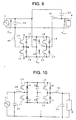
- FIG. 10 is a block circuit diagram of a conventional electric power converter for converting AC electric power to DC electric power once and for converting the converted DC electric power back to AC electric power.
- a series circuit consisting of semiconductor switching devices 10 and 11 is connected to an end of an AC power supply 1 via a reactor 40.
- Diodes 14 and 15 are connected in antiparallel connection to the semiconductor switching devices 10 and 11, respectively.
- the semiconductor switching devices 10 and 11, controlled by PWM (pulse width modulation), work together with the diodes 14 and 15 as a rectifier circuit that conducts control and conversion operations for storing energy in capacitors 30 and 31 connected in series to each other so that the voltages of the capacitors 30 and 31 may be DC voltages.
- PWM pulse width modulation
- a series circuit consisting of switching devices 12 and 13 is connected to the series circuit consisting of the capacitors 30 and 31.
- Diodes 16 and 17 are connected in antiparallel connection to the switching devices 12 and 13, respectively.
- a capacitor 32 connected to both ends of the AC power supply 1 works as a filter capacitor.
- a reactor 41 and a capacitor 33 connected to the input side of the load 6 constitute an LC filter.
- the conventional electric power converter described in FIG. 10 has the so-called double converter circuit configuration that converts AC electric power to DC electric power once and converts the DC electric power back to AC electric power.
- FIG. 11 is a diagram for explaining the principle of the circuit in FIG. 10.
- the converter on the side of the AC power supply 1, including the switching devices 10 and 11 and the diodes 14 and 15, works as a rectifier circuit. Therefore, one may deem, as shown in FIG. 11, the rectifier circuit described above a parallel current source 5, through which all the energy necessary for the load 6 flows.
- the converter on the side of the load 6, including the switching devices 12 and 13 and the diodes 16 and 17, works as an inverter that feeds a certain voltage to the load 6. Therefore, one may deem, as shown in FIG. 11, the inverter described above a parallel voltage source 3, through which all the energy necessary for the load 6 flows.
- the electric power converter described in the appended Claim 1 includes a series converter connected in series between an AC power supply and a load, the series converter including capacitors as the power supply thereof; a parallel converter connected in parallel to the AC power supply; the series converter compensating the change caused in the voltage of the AC power supply to keep the voltage fed to the load at a certain value; and the parallel converter conducting charging and discharging operations between the AC power supply and the capacitors to compensate the voltage changes of the capacitors caused by the compensating operation of the series converter.
- the electric power converter described in the appended Claim 2 is obtained by providing the electric power converter described in the appended Claim 1 with the following constituent elements:
- the electric power converter described in the appended Claim 3 is obtained by providing the electric power converter described in the appended Claim 2 with the following constituent elements:
- the electric power converter described in the appended Claim 4 is obtained by providing the electric power converter described in the appended Claim 2 or 3 with the following constituent elements:
- the electric power converter described in the appended Claim 5 is obtained by providing the electric power converter described in the appended Claim 2 or 3 with the following constituent elements:
- the electric power converter described in the appended Claim 6 is obtained by providing the electric power converter described in the appended Claim 4 with the following constituent elements:
- the electric power converter described in the appended Claim 7 is obtained by providing the electric power converter described in the appended Claim 2 or 3 with the following constituent elements:
- the electric power converter described in the appended Claim 8 is obtained by providing the electric power converter described in the appended Claim 4 with the following constituent elements:
- the electric power converter described in the appended Claim 9 is obtained by providing the electric power converter described in the appended Claim 5 with the following constituent elements:
- the electric power converter described in the appended Claim 10 is obtained by changing the connection position of the fourth capacitor described in the appended Claim 2.
- the electric power converter described in the appended Claim 10 is obtained by providing the electric power converter described in the appended Claim 1 with the following constituent elements:
- the electric power converter described in the appended Claim 11 is obtained by providing the electric power converter described in the appended Claim 10 with the following constituent elements:
- the electric power converter described in the appended Claim 12 is obtained by providing the electric power converter described in the appended Claim 10 or 11 with the following constituent elements:
- the electric power converter described in the appended Claim 13 is obtained by providing the electric power converter described in the appended Claim 10 or 11 with the following constituent elements:
- the electric power converter described in the appended Claim 14 is obtained by providing the electric power converter described in the appended Claim 12 with the following constituent elements:
- FIG. 1 is a block circuit diagram of an electric power converter according to the first embodiment of the invention.
- the electric power converter according to the first embodiment corresponds to the subject matters of the appended Claims 1 and 2.
- the electric power converter according to the first embodiment includes a series circuit including an IGBT (insulated gate bipolar transistor) and such a first semiconductor switching device 10, to which a first diode 14 is connected in antiparallel connection, and an IGBT and such a second semiconductor switching device 11, to which a second diode 15 is connected in antiparallel connection.
- IGBT insulated gate bipolar transistor
- the electric power converter according to the first embodiment includes also a series circuit including a third semiconductor switching device 12, to which a third diode 16 is connected in antiparallel connection, and a fourth semiconductor switching device 13, to which a fourth diode 17 is connected in antiparallel connection.
- the electric power converter according to the first embodiment includes also a series circuit including a first capacitor 30 and a second capacitor 31.
- the first series switch circuit, the second series switch circuit, and the series capacitor circuit are connected in parallel to each other.
- a third capacitor 32 is connected in parallel to an AC power supply 1.
- a fourth capacitor 33 is connected in parallel to a load 6.
- An end of the AC power supply 1 is connected to an end of the load 6 and the other end the AC power supply 1 is connected to the series connection point of the capacitors 30 and 31.
- the connection point of the AC power supply 1 and the load 6 is connected to the series connection point of the first and second switching devices 10 and 11 via a first reactor 40.
- the other end of the load 6 is connected to the series connection point of the third and fourth switching devices 12 and 13 via a second reactor 41.
- the capacitors 30, 31, the switching devices 12, 13, and the diodes 16, 17 are connected in series between the AC power supply 1 and the load 6.
- the series circuit including the capacitors 30, 31, the switching devices 12, 13, and the diodes 16, 17 will be referred to as the "series converter”.
- the capacitors 30, 31, the switching devices 10, 11, and the diodes 14, 15 are connected in parallel to the AC power supply 1.
- the parallel circuit including the capacitors 30, 31, the switching devices 10, 11, and the diodes 14, 15 will be referred to as the "parallel converter”.
- FIG. 2 is a diagram for explaining the principle of the electric power converter in FIG. 1.
- a parallel compensation current source 4 represents the parallel converter described above and a series compensation voltage source 2 the series converter described above.
- the series compensation voltage source 2 When the series compensation voltage source 2 generates an arbitrary voltage, the sum of the voltage from the AC power supply 1 (the AC voltage source) and the voltage from the series compensation voltage source 2 is applied to the load 6. Therefore, even when the voltage of the AC power supply 1 varies (e.g. drops), a certain voltage is fed to the load 6 by compensating the voltage drop by adding the variable voltage from the series compensation voltage source 2 to the voltage of the AC power supply 1.
- the potential of the point P is the potential obtained by superposing the voltage V 30 of the capacitor 30 on the potential of the point M in FIG. 1 (the voltage Vin of the AC power supply 1).
- the potential of the point N is the potential obtained by superposing the voltage V 31 of the capacitor 31 on the potential of the point M in FIG. 1.
- the chopping by on-off control of the switching devices 12 and 13 is conducted by the PWM control that controls the voltage Vout across the load 6 at a reference value or by the PWM control that controls the voltage added to or subtracted from the potential of the point M at a reference value.
- the power supply controlled by PWM is capable of shaping the voltage fed to the load 6 with a sinusoidal waveform or with an arbitrary waveform, if necessary.
- the parallel converter (parallel compensation current source 4) conducts charging and discharging operations between the AC power supply 1 and the capacitors 30 and 31 to compensate the voltage changes (drop and rise) of the capacitors 30 and 31 caused by the operations of the series converter (series compensation power supply 2).
- the energy fed to the load 6 flows only through the series converter. Only the energy used for the voltage compensation by the series converter flows through the parallel converter. Therefore, the losses caused by the parallel converter are reduced as compared with the conventional double converter configuration and the conversion efficiency of the entire electric power converter is improved.
- FIG. 4 is a block circuit diagram of an electric power converter according to the second embodiment of the invention.
- the electric power converter according to the second embodiment corresponds to the subject matter of the appended Claim 3.
- the main circuit configuration of the electric power converter according to the second embodiment shown in FIG. 4 is substantially identical with the main circuit configuration of the electric power converter according to the first embodiment shown in FIG. 1.
- the electric power converter according to the second embodiment is different from the electric power converter according to the first embodiment in that the electric power converter according to the second embodiment includes a voltage detecting means 70 for detecting the voltage Vin across the AC power supply 1, the voltage V M (V MN ) of the pint M on the basis of the potential of the point N, the voltage V P (V PN ) of the pint P on the basis of the potential of the point N, and the voltage Vout, a current detecting means 71 for detecting the current flowing through the reactor 40, and a voltage and reactor current control means 72 for controlling the output voltage and for controlling the current flowing,through the reactor 40.
- the voltage Vin across the AC power supply 1 detected by the voltage detecting means 70 is used as a reference sinusoidal wave.
- the current, flowing through the reactor 40 and detected by the current detecting means 71, is controlled on the basis of the reference sinusoidal wave by the voltage and reactor current control means 72 so that the current flowing through the reactor 40 may be sinusoidal.
- the circuit shown in FIG. 1 feeds a sinusoidal voltage Vout to the load 6, a sinusoidal current is made to flow following the sinusoidal voltage.
- FIG. 5 is a block circuit diagram of an electric power converter according to the third embodiment of the invention.
- the electric power converter according to the third embodiment corresponds to the subject matter of the appended Claim 4.
- the electric power converter according to the third embodiment is different from the electric power converter according to the first embodiment in that the electric power converter according to the third embodiment includes a changeover switch 50 having a first changeover contact 52, a second changeover contact 53 and a common terminal 51. An end of the load 6 is connected to the common terminal 51.
- the series connection point of the capacitors 30 and 31 is connected to the first changeover contact 52.
- the connection point of the reactor 41 and the capacitor 33 is connected to the second changeover contact 53.
- FIG. 6 is a block circuit diagram of an electric power converter according to the fourth embodiment of the invention.
- the electric power converter according to the fourth embodiment corresponds to the subject matter of the appended Claim 6.
- the electric power converter according to the fourth embodiment includes an energy storage element 60 connected in parallel between the points P and N via a charging and discharging means 61.
- the energy storage element 60 and the charging and discharging means 61 are added exemplary to the circuit shown in FIG. 5, the energy storage element 60 and the charging and discharging means 61 may be added to the circuits shown in FIGs. 1 and 4 with no problem.
- the circuits of FIGs. 1 and 4, to which the energy storage element 60 and the charging and discharging means 61 are added, correspond to the subject matter of the appended Claim 5.
- the charging and discharging means 61 is formed of a combination of a semiconductor switch and a magnetic component part such as a reactor.
- a battery and such a secondary cell or a flywheel may be used for the energy storage element 60.
- the circuit configuration according to the fourth embodiment facilitates using the parallel converter and the series converter continuously to keep feeding a desired voltage stably to the load 6 even when the anomaly of the AC power supply 1 is caused.
- FIG. 7 is a block circuit diagram of an electric power converter according to the fifth embodiment of the invention.
- the electric power converter according to the fifth embodiment corresponds to the subject matter of the appended Claim 6.
- the electric power converter according to the fifth embodiment divides the charging and discharging means 61 into a charging means 62 and a discharging means 63.
- the charging means 62 is connected to both ends of the AC power supply 1.
- the discharging means 63 is connected between the points P and N.
- the energy storage element 60 is connected in parallel to the charging means 62 and the discharging means 63.
- the charging means 62, the discharging means 63, and the energy storage element 60 may be added to the circuit configurations shown in FIGs. 1 and 4 with no problem.
- the circuits of FIGS. 1 and 4, to which the charging means 62, the discharging means 63, and the energy storage element 60 are added, correspond to the subject matter of the appended Claim 5.
- the charging means 62 charges up the energy storage element 60 while the AC power supply 1 is working normally.
- the energy stored in the energy storage element 60 is fed to the capacitors 30 and 31 using the discharging means 63.
- the parallel converter and the series converter are made to work using the energy fed to the capacitors 30 and 31 to feed a voltage to the load 6.
- the charging means 62 and the discharging means 63 are formed of a combination of a semiconductor switch and a magnetic component part.
- the energy storage element 60 as described with reference to FIG. 6 may be used for the electric power converter according to the fifth embodiment.
- FIG. 8 is a block circuit diagram of an electric power converter according to the sixth embodiment of the invention.
- the electric power converter according to the sixth embodiment corresponds to the subject matter of the appended Claim 7.
- the reactor 41 is changed to a tapped reactor 42.
- An end of the tapped reactor 42 is connected to the series connection point of the capacitors 30 and 31.
- the other end of the tapped reactor 42 is connected to the end of the load 6 not connected to the AC power supply 1 and the series connection point of the switching devices 12 and 13.
- the end of the AC power supply 1 not connected to the load 6 is connected to the tap terminal of the tapped reactor 42.
- the circuit configuration that uses the tapped reactor 42 is applicable to the electric power converters described with reference to FIGs. 4 through 7 as described in the appended Claims 8 and 9.
- FIG. 9 is a block circuit diagram of an electric power converter according to the seventh embodiment of the invention.
- the electric power converter according to the seventh embodiment corresponds to the subject matter of the appended Claim 10.
- the circuit configuration according to the seventh embodiment changes the connection point of the fourth capacitor 33 in FIG. 1.
- the fourth capacitor 33 is connected between the connection point of the load 6 and the second reactor 41 and the series connection point of the first and second capacitors 30 and 31.
- the capacitors 30, 31, the switching devices 12, 13, and the diodes 16, 17 constitute a series converter connected in series between the AC power supply 1 and the load 6 in the same manner as described in FIG. 1.
- the capacitors 30, 31, the switching devices 10, 11, and the diodes 14, 15 constitute a parallel converter connected in parallel to the AC power supply 1.
- the first reactor 40 and the third capacitor 32 constitute an AC filter that suppresses the switching ripples of the parallel converter.
- the second reactor 41 and the fourth capacitor 33 constitute an AC filter that suppresses the switching ripples of the series converter.
- the electric power converter according to the seventh embodiment works in the same manner as the electric power converter according to the first embodiment shown in FIG. 1.
- the series compensation voltage source 2 series converter
- the voltage from the AC power supply 1 AC voltage source
- the voltage from the series compensation voltage source 2 are added to each other and applied to the load 6.
- a certain voltage is fed to the load 6 by compensating the voltage drop by adding the variable voltage from the series compensation voltage source 2 to the voltage of the AC power supply 1.
- the addition and subtraction of the series compensation voltage source 2 to and from the AC power supply 1 can be realized by the PWM control of the series converter using the capacitors 30 and 31 for the power supply thereof.
- the energy change caused by the charging and discharging of the capacitors 30 and 31 for the voltage addition and subtraction can be compensated by charging and discharging the capacitors 30 and 31 by means of the PWM control of the parallel compensation current source (parallel converter) 4 so that the total energy balance may be kept.
- the energy fed to the load 6 flows only through the series converter in the electric power converter according to the seventh embodiment too. Only the energy used for the voltage compensation by the series converter flows through the parallel converter. Therefore, the losses caused by the parallel converter are reduced as compared with the conventional double converter configuration and the conversion efficiency of the entire electric power converter is improved.
- the voltage detecting means 70, the current detecting means 71, and the voltage and reactor current control means 72 shown in FIG. 4 may be added to the circuit configuration shown in FIG. 9.
- the resulting circuit configuration corresponds to the subject matter of the appended Claim 11.
- the charging and discharging means 61 and the energy storage element 60 shown in FIG. 6 may be added to the circuit configuration shown in FIG. 9.
- the charging means 62, the discharging means 63 and the energy storage element 60 shown in FIG. 7 may be added to the circuit configuration shown in FIG. 9.
- the resulting circuit configurations correspond to the subject matter of the appended Claim 12.
- the reactor 41 in the circuit configuration shown in FIG. 9 may be replaced by the tapped reactor 42 shown in FIG. 8.
- the both ends of the tapped reactor 42 may be connected to the series connection point of the capacitors 30 and 31 and to the series connection point of the switching devices 12 and 13, and the tap terminal of the tapped reactor 42 may be connected to an end of the AC power supply 1.
- the resulting circuit configuration corresponds to the subject matter of the appended Claim 13.
- the reactor 41 in the circuit configuration shown in FIG. 9 may be replaced by the tapped reactor 42 shown in FIG. 8, and the combination of the charging and discharging means 61 and the energy storage element 60 shown in FIG. 6 or the combination of the charging means 62, the discharging means 63 and the energy storage element 60 shown in FIG. 7 may be added to the modified circuit configuration described above.
- the resulting circuit configuration corresponds to the subject matter of the appended Claim 14.
- the electric power converter according to the invention is applicable industrially as an electric power converter of the double converter type that facilitates feeding arbitrary AC electric power from an AC power supply to a load in the form of a current output by the operations of a series converter and a parallel converter.
- the electric power converter according to the invention facilitates improving the conversion efficiency by suppressing the loses caused by either one of the converters and reducing the running costs thereof.
- the electric power converter according to the invention facilitates elongating the lifetime thereof and improving the reliability thereof, since the electric power converter according to the invention employs neither electrolytic capacitor nor such a component part that should be replaced periodically.
Landscapes
- Engineering & Computer Science (AREA)
- Power Engineering (AREA)
- Rectifiers (AREA)
- Ac-Ac Conversion (AREA)
Abstract
Description
a parallel converter connected in parallel to the AC power supply;
the series converter compensating the change caused in the voltage of the AC power supply to keep the voltage fed to the load at a certain value; and
the parallel converter conducting charging and discharging operations between the AC power supply and the capacitors to compensate the voltage changes of the capacitors caused by the compensating operation of the series converter.
- FIG. 1
- is a block circuit diagram of an electric power converter according to a first embodiment of the invention.
- FIG. 2
- is a diagram for explaining the principle of the electric power converter in FIG. 1.
- FIG. 3
- is a wave chart for explaining the operations of the series converter in FIG. 1.
- FIG.4
- is a block circuit diagram of an electric power converter according to a second embodiment of the invention.
- FIG. 5
- is a block circuit diagram of an electric power converter according to a third embodiment of the invention.
- FIG. 6
- is a block circuit diagram of an electric power converter according to a fourth embodiment of the invention.
- FIG. 7
- is a block circuit diagram of an electric power converter according to a fifth embodiment of the invention.
- FIG. 8
- is a block circuit diagram of an electric power converter according to a sixth embodiment of the invention.
- FIG. 9
- is a block circuit diagram of an electric power converter according to a seventh embodiment of the invention.
- FIG. 10
- is a block circuit diagram of a conventional electric power converter for converting AC electric power to DC electric power once and for converting the converted DC electric power back to AC electric power.
- FIG. 11
- is a diagram for explaining the principle of the electric power converter in FIG. 10.
Claims (14)
- An electric power converter comprising:a series converter connected in series between an AC power supply and a load, the series converter comprising capacitors as the converter power supply thereof;a parallel converter connected in parallel to the AC power supply;the series converter compensating the change caused in the voltage of the AC power supply, whereby to keep the voltage fed to the load at a certain value; andthe parallel converter conducting charging and discharging operations between the AC power supply and the capacitors, whereby to compensate the voltage changes of the capacitors caused by the compensating operation of the series converter.
- The electric power converter according to Claim 1, comprising:a first series switch circuit comprising a first semiconductor switching device, a second semiconductor switching device, a diode connected in antiparallel connection to the first semiconductor switching device, and a diode connected in antiparallel connection to the second semiconductor switching device, the first and second semiconductor switching devices being connected in series to each other;a second series switch circuit comprising a third semiconductor switching device, a fourth semiconductor switching device, a diode connected in antiparallel connection to the third semiconductor switching device, and a diode connected in antiparallel connection to the fourth semiconductor switching device, the third and fourth semiconductor switching devices being connected in series to each other;a series capacitor circuit comprising a first capacitor and a second capacitor connected in series to each other;a third capacitor connected in parallel to the AC power supply;a fourth capacitor connected in parallel to the load;a first reactor connected between the first end of the AC power supply and the series connection point in the first series switch circuit, the first end of the AC power supply being connected to the first end of the load;a second reactor connected between the second end of the load and the series connection point in the second series switch circuit;the first series switch circuit, the second series switch circuit, and the series capacitor circuit being connected in parallel to each other, whereby to constitute a first parallel connection circuit;the second end of the AC power supply being connected to the series connection point in the series capacitor circuit;the series capacitor circuit and the second series switch circuit constituting the series converter; andthe series capacitor circuit and the first series switch circuit constituting the parallel converter.
- The electric power converter according to Claim 2, further comprising:a voltage detecting means detecting the input voltage of the electric power converter, the output voltage of the electric power converter, and the voltages in the first parallel connection circuit:a current detecting means detecting the current flowing through the first reactor;a controlling means controlling the output voltage of the electric power converter using the voltage values detected by the voltage detecting means; andthe controlling means controlling the current flowing through the first reactor using the current value detected by the current detecting means.
- The electric power converter according to Claim 2 or 3, further comprising:a changeover switch comprising a first changeover contact, a second changeover contact, and a common terminal;the connection between the second end of the load and the first end of the second reactor being disconnected;the first changeover contact being connected to the series connection point in the series capacitor circuit;the second end of the load being connected to the first end of the second reactor via the common terminal and the second changeover contact while the electric power converter is working normally; andthe common terminal being connected to the first changeover contact when an anomaly is caused in the electric power converter, whereby to feed a voltage from the AC power supply to the load.
- The electric power converter according to Claim 2 or 3, further comprising:an energy storage element; anda charging and discharging means connected to the energy storage element, whereby to feed a voltage to the load using the energy stored in the energy storage element, when the power supply voltage is anomalous.
- The electric power converter according to Claim 4, further comprising:an energy storage element; anda charging and discharging means connected to the energy storage element, whereby to feed a voltage to the load using the energy stored in the energy storage element, when the power supply voltage is anomalous.
- The electric power converter according to Claim 2 or 3, comprising:a tapped third reactor in substitution for the second reactor, the third reactor comprising a first end, a second end, and a tap terminal;the series connection point in the series capacitor circuit being connected to the first end of the third reactor;the series connection point in the second series switch circuit being connected to the second end of the load and the second end of the third reactor;the second end of the AC power supply being disconnected from the series connection point in the series capacitor circuit and connected to the tap terminal of the third reactor.
- The electric power converter according to Claim 4, comprising:a tapped third reactor in substitution for the second reactor, the third reactor comprising a first end, a second end, and a tap terminal;the series connection point in the series capacitor circuit being connected to the first end of the third reactor;the series connection point in the second series switch circuit being connected to the second end of the load and the second end of the third reactor;the second end of the AC power supply being disconnected from the series connection point in the series capacitor circuit and connected to the tap terminal of the third reactor.
- The electric power converter according to Claim 5, comprising:a tapped third reactor in substitution for the second reactor, the third reactor comprising a first end, a second end, and a tap terminal;the series connection point in the series capacitor circuit being connected to the first end of the third reactor;the series connection point in the second series switch circuit being connected to the second end of the load and the second end of the third reactor;the second end of the AC power supply being disconnected from the series connection point in the series capacitor circuit and connected to the tap terminal of the third reactor.
- The electric power converter according to Claim 1, comprising:a first series switch circuit comprising a first semiconductor switching device, a second semiconductor switching device, a diode connected in antiparallel connection to the first semiconductor switching device, and a diode connected in antiparallel connection to the second semiconductor switching device, the first and second semiconductor switching devices being connected in series to each other;a second series switch circuit comprising a third semiconductor switching device, a fourth semiconductor switching device, a diode connected in antiparallel connection to the third semiconductor switching device, and a diode connected in antiparallel connection to the fourth semiconductor switching device, the third and fourth semiconductor switching devices being connected in series to each other;a series capacitor circuit comprising a first capacitor and a second capacitor connected in series to each other;a third capacitor connected in parallel to the AC power supply;a first reactor connected between the first end of the AC power supply and the series connection point in the first series switch circuit, the first end of the AC power supply being connected to the first end of the load;a second reactor connected between the second end of the load and the series connection point in the second series switch circuit;a fourth capacitor connected between the second end of the load and the second end of the AC power supply;the first series switch circuit, the second series switch circuit, and the series capacitor circuit being connected in parallel to each other, whereby to constitute a first parallel connection circuit;the second end of the AC power supply being connected the series connection point in the series capacitor circuit;the series capacitor circuit and the second series switch circuit constituting the series converter; andthe series capacitor circuit and the first series switch circuit constituting the parallel converter.
- The electric power converter according to Claim 10, further comprising:a voltage detecting means detecting the input voltage of the electric power converter, the output voltage of the electric power converter, and the voltages in the first parallel connection circuit:a current detecting means detecting the current flowing through the first reactor;a controlling means controlling the output voltage of the electric power converter using the voltage values detected by the voltage detecting means; andthe controlling means controlling the current flowing through the first reactor using the current value detected by the current detecting means.
- The electric power converter according to Claim 10 or 11, further comprising:an energy storage element; anda charging and discharging means connected to the energy storage element, whereby to feed a voltage to the load using the energy stored in the energy storage element, when the power supply voltage is anomalous.
- The electric power converter according to Claim 10 or 11, comprising:a tapped third reactor in substitution for the second reactor, the third reactor comprising a first end, a second end, and a tap terminal;the series connection point in the series capacitor circuit being connected to the first end of the third reactor;the series connection point in the second series switch circuit being connected to the second end of the load and the second end of the third reactor;the second end of the AC power supply being disconnected from the series connection point in the series capacitor circuit and connected to the tap terminal of the third reactor.
- The electric power converter according to Claim 12, comprising:a tapped third reactor in substitution for the second reactor, the third reactor comprising a first end, a second end, and a tap terminal;the series connection point in the series capacitor circuit being connected to the first end of the third reactor;the series connection point in the second series switch circuit being connected to the second end of the load and the second end of the third reactor;the second end of the AC power supply being disconnected from the series connection point in the series capacitor circuit and connected to the tap terminal of the third reactor.
Applications Claiming Priority (5)
| Application Number | Priority Date | Filing Date | Title |
|---|---|---|---|
| JP2002161313 | 2002-06-03 | ||
| JP2002161313 | 2002-06-03 | ||
| JP2003018713 | 2003-01-28 | ||
| JP2003018713 | 2003-01-28 | ||
| PCT/JP2003/006692 WO2003103126A1 (en) | 2002-06-03 | 2003-05-28 | Power converter |
Publications (3)
| Publication Number | Publication Date |
|---|---|
| EP1511166A1 true EP1511166A1 (en) | 2005-03-02 |
| EP1511166A4 EP1511166A4 (en) | 2006-04-26 |
| EP1511166B1 EP1511166B1 (en) | 2010-10-27 |
Family
ID=29714328
Family Applications (1)
| Application Number | Title | Priority Date | Filing Date |
|---|---|---|---|
| EP03730669A Expired - Lifetime EP1511166B1 (en) | 2002-06-03 | 2003-05-28 | Power converter |
Country Status (8)
| Country | Link |
|---|---|
| US (1) | US6940734B2 (en) |
| EP (1) | EP1511166B1 (en) |
| JP (1) | JP4329692B2 (en) |
| CN (1) | CN100403642C (en) |
| AU (1) | AU2003241856A1 (en) |
| DE (1) | DE60334690D1 (en) |
| TW (1) | TWI291282B (en) |
| WO (1) | WO2003103126A1 (en) |
Families Citing this family (14)
| Publication number | Priority date | Publication date | Assignee | Title |
|---|---|---|---|---|
| JP4001060B2 (en) | 2003-02-18 | 2007-10-31 | 富士電機システムズ株式会社 | Power converter |
| JP4556516B2 (en) * | 2004-07-08 | 2010-10-06 | 富士電機システムズ株式会社 | Power converter |
| KR101158928B1 (en) * | 2005-07-09 | 2012-06-21 | 엘지전자 주식회사 | Single phase inverter |
| JP4264906B2 (en) * | 2006-06-22 | 2009-05-20 | 株式会社日立製作所 | Induction motor drive |
| ATE533220T1 (en) * | 2007-09-14 | 2011-11-15 | Abb Technology Ag | STATCOM SYSTEM FOR PROVIDING REACTIVE AND/OR ACTIVE POWER TO A POWER NETWORK |
| JP2012044824A (en) * | 2010-08-23 | 2012-03-01 | Fuji Electric Co Ltd | Power conversion device |
| JP5565527B2 (en) * | 2012-04-10 | 2014-08-06 | 富士電機株式会社 | Power converter |
| JP5527386B2 (en) * | 2012-11-08 | 2014-06-18 | 株式会社安川電機 | Current source power converter |
| JP6363391B2 (en) * | 2014-05-16 | 2018-07-25 | 株式会社東芝 | Voltage regulator |
| EP3220531B1 (en) * | 2014-11-11 | 2024-09-25 | Mitsubishi Electric Corporation | Power conversion device |
| JP2020167747A (en) * | 2017-07-31 | 2020-10-08 | 日本電産株式会社 | Power supply device, driving device, control method, and program |
| GB2573318B (en) * | 2018-05-03 | 2020-06-10 | Zhong Qingchang | SYNDEM converter |
| US10530267B1 (en) * | 2019-01-15 | 2020-01-07 | Cotek Electronic Ind. Co., Ltd. | Power converter |
| GB2586343B (en) * | 2020-07-07 | 2024-03-13 | Zhong Qingchang | Power electronic converter with a ground fault detection unit that shares a common ground with both DC ports and AC ports |
Family Cites Families (16)
| Publication number | Priority date | Publication date | Assignee | Title |
|---|---|---|---|---|
| US4651265A (en) * | 1985-07-29 | 1987-03-17 | Westinghouse Electric Corp. | Active power conditioner system |
| DE68922049T2 (en) * | 1988-09-06 | 1995-09-21 | Toshiba Kawasaki Kk | Pulse-width modulated power supply with the ability to suppress modulation frequency signal components of earth potentials. |
| JP2677409B2 (en) * | 1988-09-19 | 1997-11-17 | 勲 高橋 | Inverter device |
| US5017800A (en) * | 1989-09-29 | 1991-05-21 | Wisconsin Alumni Research Foundation | AC to DC to AC power conversion apparatus with few active switches and input and output control |
| JPH03230764A (en) * | 1990-02-01 | 1991-10-14 | Toshiba Corp | Power supply device using pwm control |
| US5099410A (en) * | 1990-11-13 | 1992-03-24 | Wisconsin Alumni Research Foundation | Single phase ac power conversion apparatus |
| ES2070051B1 (en) * | 1992-11-27 | 1997-02-16 | Ingenieria De Sistemas De Cont | STATIC ENERGY REGULATOR FOR LIGHTING NETWORKS WITH CONTROL OVER THE MAGNITUDE OF INTENSITY AND / OR VOLTAGE, HARMONIC CONTENT AND REACTIVE ENERGY SUPPLIED WITH THE LOAD. |
| JP2918430B2 (en) * | 1993-04-02 | 1999-07-12 | 三菱電機株式会社 | Power converter |
| FR2713030B1 (en) * | 1993-11-24 | 1996-01-12 | Merlin Gerin | Uninterruptible feed through neutral through, comprising a double chopper-elevator. |
| JP3203464B2 (en) * | 1994-06-11 | 2001-08-27 | サンケン電気株式会社 | AC power converter |
| US6084785A (en) * | 1997-03-19 | 2000-07-04 | Hitachi, Ltd. | Electric power converter |
| US6118676A (en) * | 1998-11-06 | 2000-09-12 | Soft Switching Technologies Corp. | Dynamic voltage sag correction |
| JP3296425B2 (en) * | 1999-03-10 | 2002-07-02 | サンケン電気株式会社 | Power converter |
| TW513850B (en) * | 2000-04-03 | 2002-12-11 | Shan Ken Oenki Kabushiki Kaish | Electric power converting apparatus |
| US6671191B2 (en) * | 2001-03-22 | 2003-12-30 | Sanyo Denki Co., Ltd. | Electric power conversion apparatus |
| TW546897B (en) * | 2001-08-31 | 2003-08-11 | Delta Electronics Inc | Electronic circuit apparatus having suppression of harmonics and voltage stabilization function and control method |
-
2003
- 2003-05-27 TW TW092114310A patent/TWI291282B/en not_active IP Right Cessation
- 2003-05-28 CN CNB038010429A patent/CN100403642C/en not_active Expired - Lifetime
- 2003-05-28 JP JP2004510098A patent/JP4329692B2/en not_active Expired - Lifetime
- 2003-05-28 AU AU2003241856A patent/AU2003241856A1/en not_active Abandoned
- 2003-05-28 US US10/487,768 patent/US6940734B2/en not_active Expired - Lifetime
- 2003-05-28 EP EP03730669A patent/EP1511166B1/en not_active Expired - Lifetime
- 2003-05-28 WO PCT/JP2003/006692 patent/WO2003103126A1/en not_active Ceased
- 2003-05-28 DE DE60334690T patent/DE60334690D1/en not_active Expired - Lifetime
Also Published As
| Publication number | Publication date |
|---|---|
| US20040233688A1 (en) | 2004-11-25 |
| EP1511166A4 (en) | 2006-04-26 |
| JP4329692B2 (en) | 2009-09-09 |
| DE60334690D1 (en) | 2010-12-09 |
| CN100403642C (en) | 2008-07-16 |
| TWI291282B (en) | 2007-12-11 |
| WO2003103126A1 (en) | 2003-12-11 |
| TW200402928A (en) | 2004-02-16 |
| US6940734B2 (en) | 2005-09-06 |
| EP1511166B1 (en) | 2010-10-27 |
| CN1557044A (en) | 2004-12-22 |
| AU2003241856A1 (en) | 2003-12-19 |
| JPWO2003103126A1 (en) | 2005-10-06 |
Similar Documents
| Publication | Publication Date | Title |
|---|---|---|
| JP5565527B2 (en) | Power converter | |
| US10211719B2 (en) | Power converter | |
| US7391132B2 (en) | Methods and apparatus providing double conversion/series-parallel hybrid operation in uninterruptible power supplies | |
| US9007040B2 (en) | DC-DC power conversion apparatus | |
| US9438115B2 (en) | Power supply system | |
| US9041251B2 (en) | Boost converter with multiple inputs and inverter circuit | |
| US7964990B2 (en) | Power supply apparatus | |
| EP2533408B1 (en) | Power supply arrangement for single ended class D amplifier | |
| EP2827487B1 (en) | Power conversion apparatus | |
| US8174849B2 (en) | Electric power converter with soft switching for two way power conversion | |
| EP1511166A1 (en) | Power converter | |
| WO2007110954A1 (en) | Power supply apparatus | |
| US20230074022A1 (en) | Power converter topologies with power factor correction circuits controlled using adjustable deadtime | |
| CN101383514A (en) | UPS | |
| US6940188B2 (en) | Electric power converting device | |
| KR20230004649A (en) | DC-DC converter assembly | |
| US20230076369A1 (en) | Unidirectional power converters with power factor correction circuits controlled using adjustable deadtime | |
| EP2517345B1 (en) | Groundable dc/dc converter | |
| EP2824818B1 (en) | Power converter | |
| US20050269882A1 (en) | Uninterruptible power supply | |
| US9294008B2 (en) | Two-quadrant chopper | |
| Rodriguez et al. | Three-port power electronic system for energy storage and recovery using a parallel connection of a power factor corrector boost and a dual active bridge | |
| JP2017175689A (en) | Power conversion apparatus |
Legal Events
| Date | Code | Title | Description |
|---|---|---|---|
| PUAI | Public reference made under article 153(3) epc to a published international application that has entered the european phase |
Free format text: ORIGINAL CODE: 0009012 |
|
| 17P | Request for examination filed |
Effective date: 20040226 |
|
| AK | Designated contracting states |
Kind code of ref document: A1 Designated state(s): AT BE BG CH CY CZ DE DK EE ES FI FR GB GR HU IE IT LI LU MC NL PT RO SE SI SK TR |
|
| AX | Request for extension of the european patent |
Extension state: AL LT LV MK |
|
| DAX | Request for extension of the european patent (deleted) | ||
| RBV | Designated contracting states (corrected) |
Designated state(s): AT BE BG DE FR GB |
|
| A4 | Supplementary search report drawn up and despatched |
Effective date: 20060313 |
|
| 17Q | First examination report despatched |
Effective date: 20090904 |
|
| GRAP | Despatch of communication of intention to grant a patent |
Free format text: ORIGINAL CODE: EPIDOSNIGR1 |
|
| GRAS | Grant fee paid |
Free format text: ORIGINAL CODE: EPIDOSNIGR3 |
|
| GRAA | (expected) grant |
Free format text: ORIGINAL CODE: 0009210 |
|
| AK | Designated contracting states |
Kind code of ref document: B1 Designated state(s): DE FR GB |
|
| REG | Reference to a national code |
Ref country code: GB Ref legal event code: FG4D |
|
| REF | Corresponds to: |
Ref document number: 60334690 Country of ref document: DE Date of ref document: 20101209 Kind code of ref document: P |
|
| PLBE | No opposition filed within time limit |
Free format text: ORIGINAL CODE: 0009261 |
|
| STAA | Information on the status of an ep patent application or granted ep patent |
Free format text: STATUS: NO OPPOSITION FILED WITHIN TIME LIMIT |
|
| 26N | No opposition filed |
Effective date: 20110728 |
|
| REG | Reference to a national code |
Ref country code: DE Ref legal event code: R097 Ref document number: 60334690 Country of ref document: DE Effective date: 20110728 |
|
| REG | Reference to a national code |
Ref country code: DE Ref legal event code: R081 Ref document number: 60334690 Country of ref document: DE Owner name: FUJI ELECTRIC CO., LTD., JP Free format text: FORMER OWNER: FUJI ELECTRIC HOLDINGS CO., LTD., KAWASAKI, JP Effective date: 20111208 Ref country code: DE Ref legal event code: R082 Ref document number: 60334690 Country of ref document: DE Representative=s name: MERH-IP MATIAS ERNY REICHL HOFFMANN, DE Effective date: 20111208 Ref country code: DE Ref legal event code: R081 Ref document number: 60334690 Country of ref document: DE Owner name: FUJI ELECTRIC CO., LTD., KAWASAKI-SHI, JP Free format text: FORMER OWNER: FUJI ELECTRIC HOLDINGS CO., LTD., KAWASAKI, JP Effective date: 20111208 Ref country code: DE Ref legal event code: R082 Ref document number: 60334690 Country of ref document: DE Representative=s name: MERH-IP MATIAS ERNY REICHL HOFFMANN PATENTANWA, DE Effective date: 20111208 |
|
| REG | Reference to a national code |
Ref country code: FR Ref legal event code: PLFP Year of fee payment: 14 |
|
| REG | Reference to a national code |
Ref country code: FR Ref legal event code: PLFP Year of fee payment: 15 |
|
| REG | Reference to a national code |
Ref country code: FR Ref legal event code: PLFP Year of fee payment: 16 |
|
| PGFP | Annual fee paid to national office [announced via postgrant information from national office to epo] |
Ref country code: GB Payment date: 20220407 Year of fee payment: 20 Ref country code: FR Payment date: 20220408 Year of fee payment: 20 Ref country code: DE Payment date: 20220406 Year of fee payment: 20 |
|
| REG | Reference to a national code |
Ref country code: DE Ref legal event code: R071 Ref document number: 60334690 Country of ref document: DE |
|
| REG | Reference to a national code |
Ref country code: GB Ref legal event code: PE20 Expiry date: 20230527 |
|
| PG25 | Lapsed in a contracting state [announced via postgrant information from national office to epo] |
Ref country code: GB Free format text: LAPSE BECAUSE OF EXPIRATION OF PROTECTION Effective date: 20230527 |