EP1511091B1 - Nitride-based light emitting device, and method of manufacturing the same - Google Patents
Nitride-based light emitting device, and method of manufacturing the same Download PDFInfo
- Publication number
- EP1511091B1 EP1511091B1 EP04254402.3A EP04254402A EP1511091B1 EP 1511091 B1 EP1511091 B1 EP 1511091B1 EP 04254402 A EP04254402 A EP 04254402A EP 1511091 B1 EP1511091 B1 EP 1511091B1
- Authority
- EP
- European Patent Office
- Prior art keywords
- layer
- metal
- light emitting
- type clad
- metal layer
- Prior art date
- Legal status (The legal status is an assumption and is not a legal conclusion. Google has not performed a legal analysis and makes no representation as to the accuracy of the status listed.)
- Active
Links
- 150000004767 nitrides Chemical class 0.000 title claims description 16
- 238000004519 manufacturing process Methods 0.000 title claims description 11
- 229910052751 metal Inorganic materials 0.000 claims description 124
- 239000002184 metal Substances 0.000 claims description 124
- PXHVJJICTQNCMI-UHFFFAOYSA-N Nickel Chemical compound [Ni] PXHVJJICTQNCMI-UHFFFAOYSA-N 0.000 claims description 36
- 229910052709 silver Inorganic materials 0.000 claims description 28
- 239000004332 silver Substances 0.000 claims description 28
- 238000000034 method Methods 0.000 claims description 21
- 239000000758 substrate Substances 0.000 claims description 18
- 229910052759 nickel Inorganic materials 0.000 claims description 17
- KDLHZDBZIXYQEI-UHFFFAOYSA-N Palladium Chemical compound [Pd] KDLHZDBZIXYQEI-UHFFFAOYSA-N 0.000 claims description 16
- 238000000137 annealing Methods 0.000 claims description 16
- BASFCYQUMIYNBI-UHFFFAOYSA-N platinum Chemical compound [Pt] BASFCYQUMIYNBI-UHFFFAOYSA-N 0.000 claims description 16
- ATJFFYVFTNAWJD-UHFFFAOYSA-N Tin Chemical compound [Sn] ATJFFYVFTNAWJD-UHFFFAOYSA-N 0.000 claims description 15
- 239000010948 rhodium Substances 0.000 claims description 15
- 229910052718 tin Inorganic materials 0.000 claims description 15
- 239000003570 air Substances 0.000 claims description 14
- 229910052703 rhodium Inorganic materials 0.000 claims description 12
- MHOVAHRLVXNVSD-UHFFFAOYSA-N rhodium atom Chemical compound [Rh] MHOVAHRLVXNVSD-UHFFFAOYSA-N 0.000 claims description 12
- 239000010949 copper Substances 0.000 claims description 9
- QVGXLLKOCUKJST-UHFFFAOYSA-N atomic oxygen Chemical compound [O] QVGXLLKOCUKJST-UHFFFAOYSA-N 0.000 claims description 8
- RYGMFSIKBFXOCR-UHFFFAOYSA-N Copper Chemical compound [Cu] RYGMFSIKBFXOCR-UHFFFAOYSA-N 0.000 claims description 7
- KJTLSVCANCCWHF-UHFFFAOYSA-N Ruthenium Chemical compound [Ru] KJTLSVCANCCWHF-UHFFFAOYSA-N 0.000 claims description 7
- 239000010941 cobalt Substances 0.000 claims description 7
- 229910017052 cobalt Inorganic materials 0.000 claims description 7
- GUTLYIVDDKVIGB-UHFFFAOYSA-N cobalt atom Chemical compound [Co] GUTLYIVDDKVIGB-UHFFFAOYSA-N 0.000 claims description 7
- 229910052802 copper Inorganic materials 0.000 claims description 7
- 229910052741 iridium Inorganic materials 0.000 claims description 7
- GKOZUEZYRPOHIO-UHFFFAOYSA-N iridium atom Chemical compound [Ir] GKOZUEZYRPOHIO-UHFFFAOYSA-N 0.000 claims description 7
- 229910052746 lanthanum Inorganic materials 0.000 claims description 7
- FZLIPJUXYLNCLC-UHFFFAOYSA-N lanthanum atom Chemical compound [La] FZLIPJUXYLNCLC-UHFFFAOYSA-N 0.000 claims description 7
- 229910052760 oxygen Inorganic materials 0.000 claims description 7
- 239000001301 oxygen Substances 0.000 claims description 7
- 229910052763 palladium Inorganic materials 0.000 claims description 7
- 229910052697 platinum Inorganic materials 0.000 claims description 7
- 229910052702 rhenium Inorganic materials 0.000 claims description 7
- WUAPFZMCVAUBPE-UHFFFAOYSA-N rhenium atom Chemical compound [Re] WUAPFZMCVAUBPE-UHFFFAOYSA-N 0.000 claims description 7
- 229910052707 ruthenium Inorganic materials 0.000 claims description 7
- WFKWXMTUELFFGS-UHFFFAOYSA-N tungsten Chemical compound [W] WFKWXMTUELFFGS-UHFFFAOYSA-N 0.000 claims description 7
- 229910052721 tungsten Inorganic materials 0.000 claims description 7
- 239000010937 tungsten Substances 0.000 claims description 7
- 229910052725 zinc Inorganic materials 0.000 claims description 7
- 239000011701 zinc Substances 0.000 claims description 7
- XKRFYHLGVUSROY-UHFFFAOYSA-N Argon Chemical compound [Ar] XKRFYHLGVUSROY-UHFFFAOYSA-N 0.000 claims description 6
- IJGRMHOSHXDMSA-UHFFFAOYSA-N Atomic nitrogen Chemical compound N#N IJGRMHOSHXDMSA-UHFFFAOYSA-N 0.000 claims description 6
- 239000000463 material Substances 0.000 claims description 6
- HCHKCACWOHOZIP-UHFFFAOYSA-N Zinc Chemical compound [Zn] HCHKCACWOHOZIP-UHFFFAOYSA-N 0.000 claims description 5
- 229910052715 tantalum Inorganic materials 0.000 claims description 5
- GUVRBAGPIYLISA-UHFFFAOYSA-N tantalum atom Chemical compound [Ta] GUVRBAGPIYLISA-UHFFFAOYSA-N 0.000 claims description 5
- 230000005540 biological transmission Effects 0.000 claims description 4
- 229910052594 sapphire Inorganic materials 0.000 claims description 4
- 239000010980 sapphire Substances 0.000 claims description 4
- 229910052786 argon Inorganic materials 0.000 claims description 3
- 239000007789 gas Substances 0.000 claims description 3
- 229910052734 helium Inorganic materials 0.000 claims description 3
- 239000001307 helium Substances 0.000 claims description 3
- SWQJXJOGLNCZEY-UHFFFAOYSA-N helium atom Chemical compound [He] SWQJXJOGLNCZEY-UHFFFAOYSA-N 0.000 claims description 3
- 239000001257 hydrogen Substances 0.000 claims description 3
- 229910052739 hydrogen Inorganic materials 0.000 claims description 3
- 229910052738 indium Inorganic materials 0.000 claims description 3
- APFVFJFRJDLVQX-UHFFFAOYSA-N indium atom Chemical compound [In] APFVFJFRJDLVQX-UHFFFAOYSA-N 0.000 claims description 3
- 229910052757 nitrogen Inorganic materials 0.000 claims description 3
- 125000004435 hydrogen atom Chemical class [H]* 0.000 claims 1
- 239000010410 layer Substances 0.000 description 205
- BQCADISMDOOEFD-UHFFFAOYSA-N Silver Chemical compound [Ag] BQCADISMDOOEFD-UHFFFAOYSA-N 0.000 description 26
- JMASRVWKEDWRBT-UHFFFAOYSA-N Gallium nitride Chemical compound [Ga]#N JMASRVWKEDWRBT-UHFFFAOYSA-N 0.000 description 17
- 229910002601 GaN Inorganic materials 0.000 description 13
- 229910044991 metal oxide Inorganic materials 0.000 description 10
- 150000004706 metal oxides Chemical class 0.000 description 10
- 229910000990 Ni alloy Inorganic materials 0.000 description 8
- 239000002019 doping agent Substances 0.000 description 8
- 239000002075 main ingredient Substances 0.000 description 8
- QELJHCBNGDEXLD-UHFFFAOYSA-N nickel zinc Chemical compound [Ni].[Zn] QELJHCBNGDEXLD-UHFFFAOYSA-N 0.000 description 8
- CSCPPACGZOOCGX-UHFFFAOYSA-N Acetone Chemical compound CC(C)=O CSCPPACGZOOCGX-UHFFFAOYSA-N 0.000 description 7
- XLOMVQKBTHCTTD-UHFFFAOYSA-N Zinc monoxide Chemical compound [Zn]=O XLOMVQKBTHCTTD-UHFFFAOYSA-N 0.000 description 7
- 150000001875 compounds Chemical class 0.000 description 6
- 239000010931 gold Substances 0.000 description 6
- 230000008569 process Effects 0.000 description 6
- GYHNNYVSQQEPJS-UHFFFAOYSA-N Gallium Chemical compound [Ga] GYHNNYVSQQEPJS-UHFFFAOYSA-N 0.000 description 5
- 230000004888 barrier function Effects 0.000 description 5
- 238000006243 chemical reaction Methods 0.000 description 5
- 229910052733 gallium Inorganic materials 0.000 description 5
- 229910000480 nickel oxide Inorganic materials 0.000 description 5
- 229910045601 alloy Inorganic materials 0.000 description 4
- 239000000956 alloy Substances 0.000 description 4
- PCHJSUWPFVWCPO-UHFFFAOYSA-N gold Chemical compound [Au] PCHJSUWPFVWCPO-UHFFFAOYSA-N 0.000 description 4
- 229910052737 gold Inorganic materials 0.000 description 4
- 229910052749 magnesium Inorganic materials 0.000 description 4
- 239000011777 magnesium Substances 0.000 description 4
- 238000005259 measurement Methods 0.000 description 4
- GNRSAWUEBMWBQH-UHFFFAOYSA-N oxonickel Chemical compound [Ni]=O GNRSAWUEBMWBQH-UHFFFAOYSA-N 0.000 description 4
- 239000004065 semiconductor Substances 0.000 description 4
- OKKJLVBELUTLKV-UHFFFAOYSA-N Methanol Chemical compound OC OKKJLVBELUTLKV-UHFFFAOYSA-N 0.000 description 3
- XAGFODPZIPBFFR-UHFFFAOYSA-N aluminium Chemical compound [Al] XAGFODPZIPBFFR-UHFFFAOYSA-N 0.000 description 3
- 238000005229 chemical vapour deposition Methods 0.000 description 3
- -1 nitride compound Chemical class 0.000 description 3
- 238000005240 physical vapour deposition Methods 0.000 description 3
- 238000004151 rapid thermal annealing Methods 0.000 description 3
- 238000002310 reflectometry Methods 0.000 description 3
- 239000011787 zinc oxide Substances 0.000 description 3
- FYYHWMGAXLPEAU-UHFFFAOYSA-N Magnesium Chemical compound [Mg] FYYHWMGAXLPEAU-UHFFFAOYSA-N 0.000 description 2
- 229910052782 aluminium Inorganic materials 0.000 description 2
- 229910052788 barium Inorganic materials 0.000 description 2
- 230000008901 benefit Effects 0.000 description 2
- 230000015572 biosynthetic process Effects 0.000 description 2
- 229910052791 calcium Inorganic materials 0.000 description 2
- 239000011575 calcium Substances 0.000 description 2
- 230000015556 catabolic process Effects 0.000 description 2
- 230000000052 comparative effect Effects 0.000 description 2
- 238000006731 degradation reaction Methods 0.000 description 2
- 238000000151 deposition Methods 0.000 description 2
- 239000012153 distilled water Substances 0.000 description 2
- 238000010894 electron beam technology Methods 0.000 description 2
- 238000000609 electron-beam lithography Methods 0.000 description 2
- 238000002474 experimental method Methods 0.000 description 2
- 239000004615 ingredient Substances 0.000 description 2
- 230000003647 oxidation Effects 0.000 description 2
- 238000007254 oxidation reaction Methods 0.000 description 2
- 239000000243 solution Substances 0.000 description 2
- 238000004544 sputter deposition Methods 0.000 description 2
- 229910052712 strontium Inorganic materials 0.000 description 2
- 238000004381 surface treatment Methods 0.000 description 2
- JBQYATWDVHIOAR-UHFFFAOYSA-N tellanylidenegermanium Chemical compound [Te]=[Ge] JBQYATWDVHIOAR-UHFFFAOYSA-N 0.000 description 2
- 230000005641 tunneling Effects 0.000 description 2
- XLYOFNOQVPJJNP-UHFFFAOYSA-N water Chemical compound O XLYOFNOQVPJJNP-UHFFFAOYSA-N 0.000 description 2
- 229910020647 Co-O Inorganic materials 0.000 description 1
- 229910020704 Co—O Inorganic materials 0.000 description 1
- UFHFLCQGNIYNRP-UHFFFAOYSA-N Hydrogen Chemical compound [H][H] UFHFLCQGNIYNRP-UHFFFAOYSA-N 0.000 description 1
- 229910019080 Mg-H Inorganic materials 0.000 description 1
- 229910018553 Ni—O Inorganic materials 0.000 description 1
- XSTXAVWGXDQKEL-UHFFFAOYSA-N Trichloroethylene Chemical group ClC=C(Cl)Cl XSTXAVWGXDQKEL-UHFFFAOYSA-N 0.000 description 1
- 239000003795 chemical substances by application Substances 0.000 description 1
- 230000018044 dehydration Effects 0.000 description 1
- 238000006297 dehydration reaction Methods 0.000 description 1
- 230000008021 deposition Effects 0.000 description 1
- 238000005137 deposition process Methods 0.000 description 1
- AJNVQOSZGJRYEI-UHFFFAOYSA-N digallium;oxygen(2-) Chemical compound [O-2].[O-2].[O-2].[Ga+3].[Ga+3] AJNVQOSZGJRYEI-UHFFFAOYSA-N 0.000 description 1
- 229910052732 germanium Inorganic materials 0.000 description 1
- 150000002431 hydrogen Chemical class 0.000 description 1
- 230000006872 improvement Effects 0.000 description 1
- 238000002347 injection Methods 0.000 description 1
- 239000007924 injection Substances 0.000 description 1
- 150000002815 nickel Chemical class 0.000 description 1
- 230000001590 oxidative effect Effects 0.000 description 1
- TWNQGVIAIRXVLR-UHFFFAOYSA-N oxo(oxoalumanyloxy)alumane Chemical compound O=[Al]O[Al]=O TWNQGVIAIRXVLR-UHFFFAOYSA-N 0.000 description 1
- 230000007420 reactivation Effects 0.000 description 1
- 230000009467 reduction Effects 0.000 description 1
- 229910052711 selenium Inorganic materials 0.000 description 1
- 229910052710 silicon Inorganic materials 0.000 description 1
- HBMJWWWQQXIZIP-UHFFFAOYSA-N silicon carbide Chemical compound [Si+]#[C-] HBMJWWWQQXIZIP-UHFFFAOYSA-N 0.000 description 1
- 239000002356 single layer Substances 0.000 description 1
- 229910052714 tellurium Inorganic materials 0.000 description 1
- 230000009466 transformation Effects 0.000 description 1
- UBOXGVDOUJQMTN-UHFFFAOYSA-N trichloroethylene Natural products ClCC(Cl)Cl UBOXGVDOUJQMTN-UHFFFAOYSA-N 0.000 description 1
Images
Classifications
-
- H—ELECTRICITY
- H01—ELECTRIC ELEMENTS
- H01L—SEMICONDUCTOR DEVICES NOT COVERED BY CLASS H10
- H01L33/00—Semiconductor devices with at least one potential-jump barrier or surface barrier specially adapted for light emission; Processes or apparatus specially adapted for the manufacture or treatment thereof or of parts thereof; Details thereof
- H01L33/36—Semiconductor devices with at least one potential-jump barrier or surface barrier specially adapted for light emission; Processes or apparatus specially adapted for the manufacture or treatment thereof or of parts thereof; Details thereof characterised by the electrodes
- H01L33/40—Materials therefor
- H01L33/405—Reflective materials
-
- H—ELECTRICITY
- H01—ELECTRIC ELEMENTS
- H01L—SEMICONDUCTOR DEVICES NOT COVERED BY CLASS H10
- H01L33/00—Semiconductor devices with at least one potential-jump barrier or surface barrier specially adapted for light emission; Processes or apparatus specially adapted for the manufacture or treatment thereof or of parts thereof; Details thereof
- H01L33/02—Semiconductor devices with at least one potential-jump barrier or surface barrier specially adapted for light emission; Processes or apparatus specially adapted for the manufacture or treatment thereof or of parts thereof; Details thereof characterised by the semiconductor bodies
- H01L33/26—Materials of the light emitting region
- H01L33/30—Materials of the light emitting region containing only elements of group III and group V of the periodic system
- H01L33/32—Materials of the light emitting region containing only elements of group III and group V of the periodic system containing nitrogen
Definitions
- the present invention relates to a nitride-based light emitting device and a method of manufacturing the same, and more particularly, to a nitride-based light emitting device having an Ohmic contact structure for increasing a quantum efficiency, and a method of manufacturing the same.
- a gallium nitride-based compound semiconductor for example, a gallium nitride (GaN) semiconductor
- GaN gallium nitride
- Ohmic contact structure between a semiconductor and an electrode is of much importance.
- a gallium nitride-based light emitting device is formed on an insulating sapphire (Al 2 O 3 ) substrate.
- the gallium nitride-based light emitting device is classified into Top-Emitting Light Emitting Diodes (TLEDs) and Flip-Chip Light Emitting Diodes (FCLEDs).
- TLEDs Top-Emitting Light Emitting Diodes
- FCLEDs Flip-Chip Light Emitting Diodes
- the top-emitting light emitting diode allows light to emit through an Ohmic electrode layer that is in contact with a P-type clad layer, and provides a low electric conductivity of the P-type clad layer to allow smooth current injection through the Ohmic electrode layer with transparency and low resistance.
- the top-emitting light emitting diode is generally employing a structure of a nickel (Ni) layer and a gold (Au) layer sequential layered on the P-type clad layer.
- the nickel layer is known in the art to form a semi-transparent Ohmic contact layer that is annealed in oxygen (O2) atmosphere to have a relative contact resistance of about 10 -3 -10 -4 ⁇ cm 2 .
- the semi-transparent Ohmic contact layer When the semi-transparent Ohmic contact layer is annealed at about 500-600°C in the oxygen atmosphere, the semi-transparent Ohmic contact layer provide a low relative contact resistance between the gold (Au) layer and a lower layer portion where the nickel oxide (NiO) is island-shaped as a P-type semiconductor oxide between the gallium nitride that forms the P-type clad layer and the nickel layer that is used as the Ohmic contact layer. Accordingly, a Schottky Barrier Height (SBH) is reduced, thereby facilitate to supply holes as a majority carrier in the vicinity of a surface of the P-type clad layer. As a result, an effective carrier concentration is increased in the vicinity of the surface of the P-type clad layer.
- SBH Schottky Barrier Height
- a reactivation process using the annealing is performed to remove a Mg-H compound to thereby increase a concentration of Magnesium dopants at a surface of the gallium nitride.
- the effective carrier concentration of above 10 19 is obtained at the surface of the P-type clad layer. Therefore, tunneling conduction is generated between the P-type clad layer and the Ohmic electrode layer that contains nickel oxide to provide an Ohmic conduction characteristic.
- the top-emitking light emitting diode using a semi-transparent electrode film formed of nickel/gold has a low optic efficiency, it is difficult to embody a large-capacity and high-luminance light emitting device.
- silver or aluminum can temporarily provide a high light-emitting efficiency due to its high reflection efficiency, but there is a drawback in that a device life is short since it is difficult to form an Ohmic contact with a lower resistance due to a small work function, and a stable device reliability is not provided since the adhesiveness with the gallium nitride is poor.
- U.S. Patent Publication No.: 2002-0190260A1 discloses a structure with nickel/silver sequential layered on the P-type clad layer, but has a drawback in that contact resistance is high, and adhesiveness is low at the time of annealing.
- WO 01/47038 describes multilayer contacts to LED devices, including GaN type lasers.
- a nitride-based light emitting device according to claim 1.
- An addition ratio of the second metal group to tin may be 0.1 to 51 atomic percentages.
- the reflective layer may be formed of silver or rhodium.
- the metal layer may include: a first metal layer formed on the P-type clad layer; and a second metal layer formed between the first metal layer and the reflective layer, the first metal layer is formed of any one of selected from the second metal group consisting of nickel, cobalt, copper, palladium, platinum, ruthenium, rhodium, iridium, tantalum, rhenium, tungsten, and a lanthanum-based metal, and the second metal layer may be formed of tin.
- the second metal layer is formed by addition of any one selected from the second metal group to any one selected from the first metal group.
- the metal layer and the reflective layer have a thickness of 0.1 nm to 10 ⁇ m.
- the N-type clad layer is formed on a substrate that is formed of light transmission material.
- the annealing may be performed at 20°C to 700°C, and the annealing may be performed in gas atmosphere containing at least one of nitrogen, argon, helium, oxygen, hydrogen, and air within a reactor in which the layer structure is installed.
- the present invention provides a nitride-based light emitting device having an electrode structure for providing a low resistance characteristic and a high reflectivity, and a method of manufacturing the same.
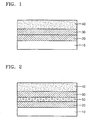
- FIG. 1 is a sectional view illustrating a P-type electrode structure with a metal layer and a reflective layer each having a different thickness.
- the P-type electrode structure includes a metal layer 30 and a reflective layer 40.
- the P-type electrode structure includes a III-group nitride-based P-type clad layer 20 formed on a substrate 10; and the metal layer 30 and the reflective layer 40 sequentially layered on the P-type clad layer 20.
- a characteristic experiment is made between the P-type clad layer 20 and the P-type electrode structure 30 and 40.
- the P-type clad layer 20 is required to have an improved Ohmic characteristic among an N-type clad layer and the P-type clad layer that face with each other centering on a light emitting layer of the III-group nitride-based light emitting-device.
- the P-type clad layer 20 uses III-group nitride compound with P-type dopants being doped.
- III-group nitride compound is expressed in a general formula Al x ln y Ga z N (0 ⁇ x ⁇ 1, 0 ⁇ y ⁇ 1, 0 ⁇ z ⁇ 1, 0 ⁇ x+y+z ⁇ 1).
- the P-type dopant can use Mg, Zn, Ca, Sr, Ba and the like.
- the metal layer 30 can employ metal or alloy that has a good reaction with the P-type clad layer 30.
- the metal layer 30 may employ metal, which can increase an effective carrier concentration of the P-type clad layer 20 and has a good primary reaction with a component, excepting for nitride, among the III-group nitride compound of the P-type clad layer 20.
- metal which can increase an effective carrier concentration of the P-type clad layer 20 and has a good primary reaction with a component, excepting for nitride, among the III-group nitride compound of the P-type clad layer 20.
- the metal layer 30 employs a GaN-based compound
- the metal layer 30 employs metal having a primary reaction with gallium (Ga) rather than nitride (N).
- the P-type clad layer 20 with a main ingredient being gallium nitride (GaN) has gallium vacancy that is formed on a surface thereof by the reaction of gallium (Ga) of the P-type clad layer 20 with the metal layer 30.
- the gallium vacancy of the P-type clad layer 20 functions as the P-type dopants to increase the effective carrier concentration on the surface of the P-type clad layer 20 by the reaction of the P-type clad layer 20 and the metal layer 30.
- the metal layer 30 satisfying the above condition is formed of any one selected from the first metal group consisting of Zinc (Zn), Indium (In) and Tin (Sn).
- the metal layer 30 can be formed of alloy that has any one main ingredient selected from the first metal group and any one additional ingredient selected from a second metal group.
- the metal layer 30 comprises tin.
- the second metal group includes Nickel (Ni), Cobalt (Co), Copper (Cu), Palladium (Pd), Platinum (Pt), Ruthenium (Ru), Rhodium (Rh), Iridium (Ir), Tantalium (Ta), Rhenium (Re), Tungsten (W), and Lanthanum (La).
- An addition ratio of the second metal group to the first metal group may be within 0.1 to 51 atomic percentages.
- the reflective layer 40 is an uppermost layer in the P-type electrode structure.
- the reflective layer 40 employs material suppressing a surface degradation, being stable against oxidation, having a non-varied characteristic, and having a high reflectivity power, at 300-600°C, which is a general temperature, in a process of manufacturing a flip-chip light emitting device.
- the reflective layer 40 may be formed of Silver (Ag) or Rhodium (Rh) that satisfies the above condition.
- the metal layer 30 and the reflective layer 40 may have a thickness of 0.1 nm to 10 ⁇ m.
- the metal layer 30 and the reflective layer 40 are formed using various well-known methods, for example, using Physical Vapor Deposition (PVD), Chemical Vapor Deposition (CVD), Plasma Laser Deposition (PLD), a dual-type thermal evaporator, sputtering and the like.
- PVD Physical Vapor Deposition
- CVD Chemical Vapor Deposition
- PLD Plasma Laser Deposition
- a dual-type thermal evaporator sputtering and the like.
- the metal layer 30 and the reflective layer 40 are generally deposited at a temperature of 20-1500°C in a reactor with a pressure of atmospheric pressure to about 10-12 torr.
- the metal layer 30 and the reflective layer 40 are annealed at 20-700°C for one second to 10 hours in a vacuum or gas atmosphere.
- the metal layer 30 and the reflective layer 40 are annealed in a reactor, at least one of nitrogen, argon, helium, oxygen, hydrogen and air is introduced into the reactor.
- a structure with the substrate 10 and the P-type clad layer 20, which is formed on the substrate and has the gallium nitride as the main ingredient is surface-cleaned at 60°C for five minutes in an ultrasonic bath using trichloroethylene, acetone, methanol, and distilled water, respectively, and then is hard-baked at 100°C for ten minutes for dehydration.
- the resultant structure is spin-coated at 400-500rpm to form a photo-resist on the P-type clad layer 20.
- the resultant is soft-baked for 15 minutes at 85°C, and a mask and a pattern are aligned to develop a mask pattern.
- the developed resultant is exposed for 15 seconds to ultraviolet (UV) with an intensity of 22.8mW, and then dipped for about 25 seconds into solution with a developing agent and the distilled water being mixed at a ratio of 1:4, for development.
- UV ultraviolet
- the developed resultant is dipped into BOE solution for five minutes so as to remove a pollution layer.
- the zinc-nickel alloy is deposited in an electron-beam evaporator to form the metal layer 30 on the P-type clad layer 20 at a thickness of 10nm, and then silver is deposited on the metal layer 30 in the electron-beam evaporator to form the reflective layer 40 at a thickness of 10nm.
- the resultant is processed in a lift-off process using acetone, and then is annealed using a Rapid Thermal Annealing (RTA) at 500°C for one minute in air atmosphere to manufacture the P-type electrode structure using Ohmic contact.
- RTA Rapid Thermal Annealing
- FIG. 2 is a sectional view illustrating a P-type electrode structure according to another embodiment of the present invention.
- a first metal layer 50, a second metal layer 30 and a reflective layer 40 are sequentially formed on a P-type clad layer 20 formed on a substrate 10.
- the P-type electrode structure includes a III-group nitride-based P-type clad layer 20 that is formed on a sapphire substrate 10; and the first metal layer 50, the second metal layer 30 and the reflective layer 40 that are sequentially layered on the P-type clad layer 20.
- a characteristic experiment is made between the P-type clad layer 20 and the P-type electrode structure.
- the first metal layer 50 may be formed of any one selected from the above-described second metal group, that is, the group consisting of Nickel (Ni), Cobalt (Co), Copper (Cu), Palladium (Pd), Platinum (Pt), Ruthenium (Ru), Rhodium (Rh), Iridium (Ir), Tantalium (Ta), Rhenium (Re), Tungsten (W), and Lanthanum (La).
- the second metal layer 30 is formed of the same material as that of the metal layer 30 described through FIG. 1 .
- the second metal layer 30 is formed of any one selected from the first metal group including Zinc (Zn), Indium (In) and Tin (Sn).
- the second metal layer 30 can be formed of any one main ingredient selected from the first metal group and any one additional ingredient selected from the above-described second metal group.
- the metal layer 30 comprises tin.
- the first metal layer 50, the second metal layer 30 and the reflective layer 40 have a total thickness of about 0.1 nm to 10 ⁇ m.
- the above P-type electrode structure performs a deposition process and an annealing process, as described above.
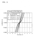
- FIGS. 3 and 4 are graphs illustrating measurement results of electrical characteristics before and after the P-type electrode structure is annealed in air atmosphere.
- the metal layer 30 is deposited using the zinc-nickel alloy on the P-type clad layer 20 and then, the reflective layer 40 is deposited using silver on the metal layer 30.
- the metal layer 30 and the reflective layer 40 are formed to have a different thickness, respectively.
- the P-type clad layer 20 has the main ingredient of the gallium nitride (GaN) with a carrier concentration of 4-5 x 10 17 cm -3 .
- FIG. 3 is a measurement result of the current-voltage characteristic in the P-type electrode structure having the metal layer 30 with a thickness of 10nm, and the reflective layer 40 with a thickness of 10nm.
- FIG. 4 is a measurement result of the current-voltage characteristic in the P-type electrode structure having the metal layer 30 with a thickness of 2.5nm, and the reflective layer 40 with a thickness of 100nm.
- the current-voltage characteristic after annealing is more improved than that before annealing, and the P-type electrode structure has a low relative contact resistance of 10 -4 to 10 -5 ⁇ cm 2 .
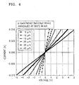
- FIG. 5 illustrates a measurement result of an Auger depth profile depending on a depth using an Auger spectroscope after the P-type electrode structure is annealed at 500°C for one minute in air atmosphere.
- the metal layer 30 is deposited using the zinc-nickel alloy on the P-type clad layer 20, and the reflective layer 40 is deposited using silver on the metal layer 30.
- the metal layer 30 and the reflective layer 40 are formed to have a thickness of 10nm, respectively.
- FIG. 6 illustrates a varied layer structure after the P-type electrode structure is annealed according to the Auger depth profile of FIG. 5 .
- the zinc oxide is diffused toward the uppermost layer to form a second metal oxide layer 31.
- a reflective layer 41 with the main ingredient being silver is located between the second metal oxide layer 31 and the first metal oxide layer 51 that contains silver.
- silver has -20 to 30 KJ/Kmole of enthalpy
- nickel has -239 KJ/Kmole
- zinc has -350.9KJ/Kmole.
- the enthalpy is energy for oxidizing metal and represents an oxidation capability. Accordingly, it can be understood that zinc and nickel are primarily oxidized at the time of annealing since they have enthalpies larger than silver by several dozens to several hundreds times.
- gallium oxide Ga 2 O 3
- metal used as the metal layer 30 is oxidized to be phase-transformed into a transparent conductive or semi-transparent conductive oxide. Accordingly, transparent conductive or semi-transparent conductive metal oxide layers 31 and 51 are formed, thereby reducing Schottky barrier height and width.
- tunneling conduction is generated at the interface between the P-type clad layer 20 and the P-type electrode structure by the gallium vacancy formed on the surface of the P-type clad layer 20, the reduction of the natural oxide, and the formation of the transparent conductive metal oxide layers 31 and 51.
- the P-type clad layer 20 functions as the dopant such that an effective hole concentration can be increased in the vicinity of the surface of the P-type clad layer 20.
- the Schottky barrier height is reduced when they are in contact with the P-type clad layer 20, thereby improving an Ohmic contact characteristic and providing transmission of almost 100%.
- the second metal oxide layer 31 being the natural oxide is formed on the surface of the uppermost layer, and the first metal oxide layer 51 being in contact with the P-type clad layer 20 is formed of the second metal group oxide (for example, Ni-O, Co-O and the like) containing silver, thereby reducing the Schottky barrier height.
- the reduced Schottky barrier height allows a high quality of Ohmic contact.
- a thick silver (Ag) layer 41 is interposed between the second metal oxide layer 31 being the zinc oxide layer and the first metal oxide layer 51 being the internally diffused second metal group oxide, thereby contributing to the conductivity improvement of nickel and functioning as an excellent reflective layer in flip-chip light emitting devices (FCLEDs).
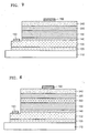
- FIG. 7 is a sectional view illustrating the light emitting device employing the P-type electrode structure of FIG. 1 according to an embodiment of the present invention.
- the light emitting device includes a substrate 110, a buffer layer 120, an N-type clad layer 130, a light emitting layer 140, a P-type clad layer 150, a metal layer 230 and a reflective layer 240 that are sequentially layered.
- Reference numeral 180 refers to a P-type electrode pad
- reference numeral 190 refers to a N-type electrode pad.
- the substrate 110 is formed of sapphire or silicon carbide (SiC).
- the buffer 120 can be omitted.
- Each layer between the buffer layer 120 to the P-type clad layer 150 is based on any compound selected from compounds expressed in the general formula Al x ln y Ga z N (0 ⁇ x ⁇ 1, 0 ⁇ y ⁇ 1, 0 ⁇ z ⁇ 1, 0 ⁇ x+y+z ⁇ 1) of the III-group nitride-based compound, and the N-type clad layer and the P-type clad layer have corresponding dopants added thereto.
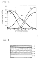
- the light emitting layer 140 can be constructed such as a single layer or a Multiple-Quantum Well (MQW) layer in the various well-known methods.
- MQW Multiple-Quantum Well
- the buffer layer 120 is formed of GaN
- the N-type clad layer 130 is formed with N-type dopants such as Si, Ge, Se, Te being added to GaN
- the P-type clad layer 150 is formed with P-type dopants such as Mg, Zn, Ca, Sr, Ba being added to GaN.
- the layers are respectively formed using various well-known deposition methods, for example, PVD, CVD, PLD, dual-type thermal evaporator, and sputtering.
- the electrode layer 230 is formed of the first metal group or the alloy having the second metal group added to the first metal group that are described above through FIG. 1 , and the reflective layer 240 is formed of silver or rhodium and then annealed.
- FIG. 8 is a sectional view illustrating a light emitting device employing a P-type electrode structure according to another embodiment of the present invention.
- the light emitting device includes a substrate 110, a buffer layer 120, an N-type clad layer 130, a light emitting layer 140, a P-type clad layer 150, a first metal layer 350, a second metal layer 330, and a reflective layer 340.
- the first metal layer 350 is formed of any one of the second metal group that is described above in FIG. 2 .
- the second metal layer 330 is formed of the first metal group or the second metal group added to the first metal group that are described above through FIG. 1 .
- the reflective layer 340 is formed of silver or rhodium.
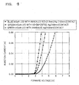
- FIG. 9 is a graph illustrating the comparative result of current-voltage characteristics of light emitting devices having the zinc-nickel alloy/silver deposited and annealed in the air atmosphere, and having only silver deposited and annealed in the air atmosphere.
- the light emitting device employing the above P-type electrode structure has an excellently improved electrical characteristic.
- a blue-light emitting diode with an InGaN structure has the metal layer 230 formed of the zinc-nickel alloy to have the thickness of 2.5nm and the reflective layer 240 formed of silver to have the thickness of 100nm.
- the above blue-light emitting diode has an operation voltage of 3.25V at 20mA.
- a blue-light emitting device having the reflective layer 240 formed of only silver at the thickness of 100nm has an operation voltage larger than the 3.25V.
- the light emitting device having only silver deposited to have the thickness of 100nm and then, annealed in the air atmosphere has the operation voltage greatly larger than before annealing, and has a considerable electrical degradation.
- the present invention describes, but is not limited to, an example of manufacturing the light emitting device.
- a surface treatment and a electron beam lithography for the P-type clad layer 150 are applied, in the same manner as the aforementioned embodiment, to the light emitting structure with the substrate, the buffer layer, the N-type clad layer, the light emitting layer and the P-type clad layer that have GaN as the main ingredient, excepting for the P-type electrode structure not yet deposited.
- the metal layer 230 is formed of the zinc-nickel alloy to have the thickness of 2.5nm, and then silver is deposited on the resultant to have the thickness of 100nm.
- the resultants is processed by the lift-off process using acetone, and then is annealed at 500°C for one minute in the air atmosphere in a rapid thermal annealing furnace. As a result, the light emitting diode is manufactured using the Ohmic contact.
- the nitride-based light emitting device and the manufacture method thereof according to the present invention provide an advantage in that the Ohmic contact characteristic with the P-type clad layer is improved to thereby enhance a wire bonding efficiency and a yield when the light emitting device is packaged, and the low relative contact resistance and the excellent current-voltage characteristic can improve a light emitting efficiency and a device life.
Description
- The present invention relates to a nitride-based light emitting device and a method of manufacturing the same, and more particularly, to a nitride-based light emitting device having an Ohmic contact structure for increasing a quantum efficiency, and a method of manufacturing the same.
- In order to embody a light emitting device such as a light emitting diode or a laser diode by using a nitride-based compound semiconductor, for example, a gallium nitride (GaN) semiconductor, Ohmic contact structure between a semiconductor and an electrode is of much importance. A gallium nitride-based light emitting device is formed on an insulating sapphire (Al2O3) substrate.
- The gallium nitride-based light emitting device is classified into Top-Emitting Light Emitting Diodes (TLEDs) and Flip-Chip Light Emitting Diodes (FCLEDs).
- The top-emitting light emitting diode allows light to emit through an Ohmic electrode layer that is in contact with a P-type clad layer, and provides a low electric conductivity of the P-type clad layer to allow smooth current injection through the Ohmic electrode layer with transparency and low resistance.
- The top-emitting light emitting diode is generally employing a structure of a nickel (Ni) layer and a gold (Au) layer sequential layered on the P-type clad layer.
- The nickel layer is known in the art to form a semi-transparent Ohmic contact layer that is annealed in oxygen (O2) atmosphere to have a relative contact resistance of about 10-3-10-4Ωcm2.
- When the semi-transparent Ohmic contact layer is annealed at about 500-600°C in the oxygen atmosphere, the semi-transparent Ohmic contact layer provide a low relative contact resistance between the gold (Au) layer and a lower layer portion where the nickel oxide (NiO) is island-shaped as a P-type semiconductor oxide between the gallium nitride that forms the P-type clad layer and the nickel layer that is used as the Ohmic contact layer. Accordingly, a Schottky Barrier Height (SBH) is reduced, thereby facilitate to supply holes as a majority carrier in the vicinity of a surface of the P-type clad layer. As a result, an effective carrier concentration is increased in the vicinity of the surface of the P-type clad layer.
- Further, after the nickel layer and the gold layer are formed on the P-type clad layer, a reactivation process using the annealing is performed to remove a Mg-H compound to thereby increase a concentration of Magnesium dopants at a surface of the gallium nitride. As a result, the effective carrier concentration of above 1019 is obtained at the surface of the P-type clad layer. Therefore, tunneling conduction is generated between the P-type clad layer and the Ohmic electrode layer that contains nickel oxide to provide an Ohmic conduction characteristic.
- However, since the top-emitking light emitting diode using a semi-transparent electrode film formed of nickel/gold has a low optic efficiency, it is difficult to embody a large-capacity and high-luminance light emitting device.
- In order to embody the large-capacity and high-luminance light emitting device, a flip-chip light emitting device using silver (Ag) or aluminum (A1) that is noticed as a high reflective material is being recently required for development.
- However, silver or aluminum can temporarily provide a high light-emitting efficiency due to its high reflection efficiency, but there is a drawback in that a device life is short since it is difficult to form an Ohmic contact with a lower resistance due to a small work function, and a stable device reliability is not provided since the adhesiveness with the gallium nitride is poor.
- In order to solve the above drawback, an Ohmic contact layer providing the high reflectivity despite the low relative contact resistance is being vigorously studied for development.
-
U.S. Patent Publication No.: 2002-0190260A1 discloses a structure with nickel/silver sequential layered on the P-type clad layer, but has a drawback in that contact resistance is high, and adhesiveness is low at the time of annealing. -
WO 01/47038 - According to an aspect of the present invention, there is provided a nitride-based light emitting device according to
claim 1. - An addition ratio of the second metal group to tin may be 0.1 to 51 atomic percentages.
- The reflective layer may be formed of silver or rhodium.
- The metal layer may include: a first metal layer formed on the P-type clad layer; and a second metal layer formed between the first metal layer and the reflective layer, the first metal layer is formed of any one of selected from the second metal group consisting of nickel, cobalt, copper, palladium, platinum, ruthenium, rhodium, iridium, tantalum, rhenium, tungsten, and a lanthanum-based metal, and the second metal layer may be formed of tin.
- The second metal layer is formed by addition of any one selected from the second metal group to any one selected from the first metal group.
- The metal layer and the reflective layer have a thickness of 0.1 nm to 10 µm.
- The N-type clad layer is formed on a substrate that is formed of light transmission material.
- In another aspect of the present invention, there is provided a method of manufacturing a nitride-based light emitting device according to
claim 10. - The annealing may be performed at 20°C to 700°C, and the annealing may be performed in gas atmosphere containing at least one of nitrogen, argon, helium, oxygen, hydrogen, and air within a reactor in which the layer structure is installed.
- The present invention provides a nitride-based light emitting device having an electrode structure for providing a low resistance characteristic and a high reflectivity, and a method of manufacturing the same.
- The above and other features and advantages of the present invention will become more apparent by describing in detail exemplary embodiments thereof with reference to the attached drawings in which:
-
FIG. 1 is a sectional view illustrating a P-type electrode structure according to an embodiment of the present invention; -
FIG. 2 is a sectional view illustrating a P-type electrode structure according to another embodiment of the present invention; -
FIGS. 3 and4 are graphs illustrating current-voltage characteristics measured before and after a P-type electrode structure ofFIG. 1 is annealed; -
FIG. 5 is a graph illustrating an Auger depth profile after a zinc-nickel alloy/silver is deposited on a P-type clad layer, and then annealed at 500°C for one minute in air atmosphere; -
FIG. 6 is a sectional view illustrating a varied layer structure after a P-type electrode structure is annealed according to an Auger depth profile ofFIG. 6 ; -
FIG. 7 is a sectional view illustrating a light emitting device employing a P-type electrode structure according to an embodiment of the present invention; -
FIG. 8 is a sectional view illustrating a light emitting device employing a P-type electrode structure according to another embodiment of the present invention; and -
FIG. 9 is a graph illustrating the comparative result of current-voltage characteristics of light emitting devices with a zinc-nickel alloy/silver deposited and annealed in air atmosphere and with only silver deposited and annealed in air atmosphere. - The present invention will now be described more fully with reference to the accompanying drawings, in which exemplary embodiments of the invention are shown. In the drawings, the thicknesses of layers and regions are exaggerated for clarity. It will also be understood that when a layer is referred to as being "on" another layer or substrate, it can be directly on the other layer or substrate, or intervening layers may also be present.
-
FIG. 1 is a sectional view illustrating a P-type electrode structure with a metal layer and a reflective layer each having a different thickness. - Referring to
FIG. 1 , the P-type electrode structure includes ametal layer 30 and areflective layer 40. - In
FIG. 1 , the P-type electrode structure includes a III-group nitride-based P-type clad layer 20 formed on asubstrate 10; and themetal layer 30 and thereflective layer 40 sequentially layered on the P-type clad layer 20. A characteristic experiment is made between the P-type clad layer 20 and the P-type electrode structure type clad layer 20 is required to have an improved Ohmic characteristic among an N-type clad layer and the P-type clad layer that face with each other centering on a light emitting layer of the III-group nitride-based light emitting-device. - The P-
type clad layer 20 uses III-group nitride compound with P-type dopants being doped. - Here, the III-group nitride compound is expressed in a general formula AlxlnyGazN (0≤ x≤ 1, 0≤ y≤ 1, 0≤ z≤ 1, 0≤ x+y+z≤ 1).
- Further, the P-type dopant can use Mg, Zn, Ca, Sr, Ba and the like.
- The
metal layer 30 can employ metal or alloy that has a good reaction with the P-type clad layer 30. - The
metal layer 30 may employ metal, which can increase an effective carrier concentration of the P-type clad layer 20 and has a good primary reaction with a component, excepting for nitride, among the III-group nitride compound of the P-type clad layer 20. For example, when themetal layer 30 employs a GaN-based compound, themetal layer 30 employs metal having a primary reaction with gallium (Ga) rather than nitride (N). - As one example, the P-
type clad layer 20 with a main ingredient being gallium nitride (GaN) has gallium vacancy that is formed on a surface thereof by the reaction of gallium (Ga) of the P-type clad layer 20 with themetal layer 30. The gallium vacancy of the P-type clad layer 20 functions as the P-type dopants to increase the effective carrier concentration on the surface of the P-type clad layer 20 by the reaction of the P-type clad layer 20 and themetal layer 30. - The
metal layer 30 satisfying the above condition is formed of any one selected from the first metal group consisting of Zinc (Zn), Indium (In) and Tin (Sn). - Otherwise, the
metal layer 30 can be formed of alloy that has any one main ingredient selected from the first metal group and any one additional ingredient selected from a second metal group. - According to the present invention, the
metal layer 30 comprises tin. - The second metal group includes Nickel (Ni), Cobalt (Co), Copper (Cu), Palladium (Pd), Platinum (Pt), Ruthenium (Ru), Rhodium (Rh), Iridium (Ir), Tantalium (Ta), Rhenium (Re), Tungsten (W), and Lanthanum (La).
- An addition ratio of the second metal group to the first metal group may be within 0.1 to 51 atomic percentages.
- The
reflective layer 40 is an uppermost layer in the P-type electrode structure. Thereflective layer 40 employs material suppressing a surface degradation, being stable against oxidation, having a non-varied characteristic, and having a high reflectivity power, at 300-600°C, which is a general temperature, in a process of manufacturing a flip-chip light emitting device. - The
reflective layer 40 may be formed of Silver (Ag) or Rhodium (Rh) that satisfies the above condition. - Furthermore, the
metal layer 30 and thereflective layer 40 may have a thickness of 0.1 nm to 10µm. - The
metal layer 30 and thereflective layer 40 are formed using various well-known methods, for example, using Physical Vapor Deposition (PVD), Chemical Vapor Deposition (CVD), Plasma Laser Deposition (PLD), a dual-type thermal evaporator, sputtering and the like. - The
metal layer 30 and thereflective layer 40 are generally deposited at a temperature of 20-1500°C in a reactor with a pressure of atmospheric pressure to about 10-12 torr. - After that, the
metal layer 30 and thereflective layer 40 are annealed at 20-700°C for one second to 10 hours in a vacuum or gas atmosphere. - When the
metal layer 30 and thereflective layer 40 are annealed in a reactor, at least one of nitrogen, argon, helium, oxygen, hydrogen and air is introduced into the reactor. - Hereinafter, a method of manufacturing the P-type electrode structure is described.
- First, a structure with the
substrate 10 and the P-type cladlayer 20, which is formed on the substrate and has the gallium nitride as the main ingredient, is surface-cleaned at 60°C for five minutes in an ultrasonic bath using trichloroethylene, acetone, methanol, and distilled water, respectively, and then is hard-baked at 100°C for ten minutes for dehydration. - After that, the resultant structure is spin-coated at 400-500rpm to form a photo-resist on the P-type clad
layer 20. Next, the resultant is soft-baked for 15 minutes at 85°C, and a mask and a pattern are aligned to develop a mask pattern. After that, the developed resultant is exposed for 15 seconds to ultraviolet (UV) with an intensity of 22.8mW, and then dipped for about 25 seconds into solution with a developing agent and the distilled water being mixed at a ratio of 1:4, for development. - Next, the developed resultant is dipped into BOE solution for five minutes so as to remove a pollution layer. The zinc-nickel alloy is deposited in an electron-beam evaporator to form the
metal layer 30 on the P-type cladlayer 20 at a thickness of 10nm, and then silver is deposited on themetal layer 30 in the electron-beam evaporator to form thereflective layer 40 at a thickness of 10nm. After that, the resultant is processed in a lift-off process using acetone, and then is annealed using a Rapid Thermal Annealing (RTA) at 500°C for one minute in air atmosphere to manufacture the P-type electrode structure using Ohmic contact. -
FIG. 2 is a sectional view illustrating a P-type electrode structure according to another embodiment of the present invention. - Elements having the same functions as those of
FIG. 1 are denoted using the same reference numerals. - Referring to
FIG. 2 , afirst metal layer 50, asecond metal layer 30 and areflective layer 40 are sequentially formed on a P-type cladlayer 20 formed on asubstrate 10. - As described above, also in
FIG. 2 , the P-type electrode structure includes a III-group nitride-based P-type cladlayer 20 that is formed on asapphire substrate 10; and thefirst metal layer 50, thesecond metal layer 30 and thereflective layer 40 that are sequentially layered on the P-type cladlayer 20. A characteristic experiment is made between the P-type cladlayer 20 and the P-type electrode structure. - The
first metal layer 50 may be formed of any one selected from the above-described second metal group, that is, the group consisting of Nickel (Ni), Cobalt (Co), Copper (Cu), Palladium (Pd), Platinum (Pt), Ruthenium (Ru), Rhodium (Rh), Iridium (Ir), Tantalium (Ta), Rhenium (Re), Tungsten (W), and Lanthanum (La). - The
second metal layer 30 is formed of the same material as that of themetal layer 30 described throughFIG. 1 . - That is, the
second metal layer 30 is formed of any one selected from the first metal group including Zinc (Zn), Indium (In) and Tin (Sn). - Otherwise, the
second metal layer 30 can be formed of any one main ingredient selected from the first metal group and any one additional ingredient selected from the above-described second metal group. - According to the present invention, the
metal layer 30 comprises tin. - The
first metal layer 50, thesecond metal layer 30 and thereflective layer 40 have a total thickness of about 0.1 nm to 10µm. - The above P-type electrode structure performs a deposition process and an annealing process, as described above.
- Hereinafter, an experimental result for the above-described P-type electrode structure that is formed on the P-type clad
layer 20 having the gallium nitride (GaN) as the main ingredient is described with reference toFIGS. 3 through 5 . -
FIGS. 3 and4 are graphs illustrating measurement results of electrical characteristics before and after the P-type electrode structure is annealed in air atmosphere. - In the P-type electrode structure, the
metal layer 30 is deposited using the zinc-nickel alloy on the P-type cladlayer 20 and then, thereflective layer 40 is deposited using silver on themetal layer 30. Themetal layer 30 and thereflective layer 40 are formed to have a different thickness, respectively. The P-type cladlayer 20 has the main ingredient of the gallium nitride (GaN) with a carrier concentration of 4-5 x 1017 cm -3. -
FIG. 3 is a measurement result of the current-voltage characteristic in the P-type electrode structure having themetal layer 30 with a thickness of 10nm, and thereflective layer 40 with a thickness of 10nm.FIG. 4 is a measurement result of the current-voltage characteristic in the P-type electrode structure having themetal layer 30 with a thickness of 2.5nm, and thereflective layer 40 with a thickness of 100nm. - As appreciated from the drawings, the current-voltage characteristic after annealing is more improved than that before annealing, and the P-type electrode structure has a low relative contact resistance of 10-4 to 10-5 Ω cm2.
- In order to analyze a cause of improving a relative contact resistance after annealing,
FIG. 5 illustrates a measurement result of an Auger depth profile depending on a depth using an Auger spectroscope after the P-type electrode structure is annealed at 500°C for one minute in air atmosphere. - In the P-type electrode structure, the
metal layer 30 is deposited using the zinc-nickel alloy on the P-type cladlayer 20, and thereflective layer 40 is deposited using silver on themetal layer 30. Themetal layer 30 and thereflective layer 40 are formed to have a thickness of 10nm, respectively. -
FIG. 6 illustrates a varied layer structure after the P-type electrode structure is annealed according to the Auger depth profile ofFIG. 5 . - As appreciated from
FIGS. 5 and 6 , external oxygen is supplied through annealing, thereby causing the phase transformation from zinc to zinc oxide and from nickel to nickel oxide. Further, the nickel oxide and silver is diffused toward the P-type cladlayer 20 to form a firstmetal oxide layer 51 that is in contact with the P-type cladlayer 20. - The zinc oxide is diffused toward the uppermost layer to form a second
metal oxide layer 31. Areflective layer 41 with the main ingredient being silver is located between the secondmetal oxide layer 31 and the firstmetal oxide layer 51 that contains silver. - At a room temperature, silver has -20 to 30 KJ/Kmole of enthalpy, nickel has -239 KJ/Kmole, and zinc has -350.9KJ/Kmole. The enthalpy is energy for oxidizing metal and represents an oxidation capability. Accordingly, it can be understood that zinc and nickel are primarily oxidized at the time of annealing since they have enthalpies larger than silver by several dozens to several hundreds times.
- The above result is caused when the annealing process is performed after the formation of the P-type clad
layer 20, and reduces gallium oxide (Ga2O3) being a natural oxide that remains on a surface of the P-type cladlayer 20 while functioning as an obstacle of carrier flow at an interface between the P-type cladlayer 20 and themetal layer 30 deposited thereon. Further, metal used as themetal layer 30 is oxidized to be phase-transformed into a transparent conductive or semi-transparent conductive oxide. Accordingly, transparent conductive or semi-transparent conductive metal oxide layers 31 and 51 are formed, thereby reducing Schottky barrier height and width. - Besides, tunneling conduction is generated at the interface between the P-type clad
layer 20 and the P-type electrode structure by the gallium vacancy formed on the surface of the P-type cladlayer 20, the reduction of the natural oxide, and the formation of the transparent conductive metal oxide layers 31 and 51. - As a result, the P-type clad
layer 20 functions as the dopant such that an effective hole concentration can be increased in the vicinity of the surface of the P-type cladlayer 20. - Further, since the zinc oxide (ZnO) formed at the time of annealing in air or oxygen atmosphere and a zinc-based or magnesium-based alloy or the metal selected from the second metal group have almost the same work function as gallium nitride, the Schottky barrier height is reduced when they are in contact with the P-type clad
layer 20, thereby improving an Ohmic contact characteristic and providing transmission of almost 100%. - Furthermore, the second
metal oxide layer 31 being the natural oxide is formed on the surface of the uppermost layer, and the firstmetal oxide layer 51 being in contact with the P-type cladlayer 20 is formed of the second metal group oxide (for example, Ni-O, Co-O and the like) containing silver, thereby reducing the Schottky barrier height. The reduced Schottky barrier height allows a high quality of Ohmic contact. At this time, a thick silver (Ag)layer 41 is interposed between the secondmetal oxide layer 31 being the zinc oxide layer and the firstmetal oxide layer 51 being the internally diffused second metal group oxide, thereby contributing to the conductivity improvement of nickel and functioning as an excellent reflective layer in flip-chip light emitting devices (FCLEDs). -
FIG. 7 is a sectional view illustrating the light emitting device employing the P-type electrode structure ofFIG. 1 according to an embodiment of the present invention. - Referring to
FIG. 7 , the light emitting device includes asubstrate 110, abuffer layer 120, an N-type cladlayer 130, alight emitting layer 140, a P-type cladlayer 150, ametal layer 230 and a reflective layer 240 that are sequentially layered. -
Reference numeral 180 refers to a P-type electrode pad, andreference numeral 190 refers to a N-type electrode pad. - The
substrate 110 is formed of sapphire or silicon carbide (SiC). - The
buffer 120 can be omitted. - Each layer between the
buffer layer 120 to the P-type cladlayer 150 is based on any compound selected from compounds expressed in the general formula AlxlnyGazN (0≤ x≤ 1, 0≤ y≤ 1, 0≤ z≤ 1, 0≤ x+y+z≤ 1) of the III-group nitride-based compound, and the N-type clad layer and the P-type clad layer have corresponding dopants added thereto. - Further, the
light emitting layer 140 can be constructed such as a single layer or a Multiple-Quantum Well (MQW) layer in the various well-known methods. - As one example, the
buffer layer 120 is formed of GaN, the N-type cladlayer 130 is formed with N-type dopants such as Si, Ge, Se, Te being added to GaN, and the P-type cladlayer 150 is formed with P-type dopants such as Mg, Zn, Ca, Sr, Ba being added to GaN. - The layers are respectively formed using various well-known deposition methods, for example, PVD, CVD, PLD, dual-type thermal evaporator, and sputtering.
- The
electrode layer 230 is formed of the first metal group or the alloy having the second metal group added to the first metal group that are described above throughFIG. 1 , and the reflective layer 240 is formed of silver or rhodium and then annealed. -
FIG. 8 is a sectional view illustrating a light emitting device employing a P-type electrode structure according to another embodiment of the present invention. - Elements having the same functions are denoted by the same reference numerals.
- Referring to
FIG. 8 , the light emitting device includes asubstrate 110, abuffer layer 120, an N-type cladlayer 130, alight emitting layer 140, a P-type cladlayer 150, afirst metal layer 350, asecond metal layer 330, and areflective layer 340. - The
first metal layer 350 is formed of any one of the second metal group that is described above inFIG. 2 . - The
second metal layer 330 is formed of the first metal group or the second metal group added to the first metal group that are described above throughFIG. 1 . - The
reflective layer 340 is formed of silver or rhodium. -
FIG. 9 is a graph illustrating the comparative result of current-voltage characteristics of light emitting devices having the zinc-nickel alloy/silver deposited and annealed in the air atmosphere, and having only silver deposited and annealed in the air atmosphere. - As appreciated in
FIG. 9 , the light emitting device employing the above P-type electrode structure has an excellently improved electrical characteristic. - That is, a blue-light emitting diode with an InGaN structure has the
metal layer 230 formed of the zinc-nickel alloy to have the thickness of 2.5nm and the reflective layer 240 formed of silver to have the thickness of 100nm. The above blue-light emitting diode has an operation voltage of 3.25V at 20mA. However, a blue-light emitting device having the reflective layer 240 formed of only silver at the thickness of 100nm has an operation voltage larger than the 3.25V. - Especially, the light emitting device having only silver deposited to have the thickness of 100nm and then, annealed in the air atmosphere has the operation voltage greatly larger than before annealing, and has a considerable electrical degradation.
- Hereinafter, the present invention describes, but is not limited to, an example of manufacturing the light emitting device.
- First, a surface treatment and a electron beam lithography for the P-type clad
layer 150 are applied, in the same manner as the aforementioned embodiment, to the light emitting structure with the substrate, the buffer layer, the N-type clad layer, the light emitting layer and the P-type clad layer that have GaN as the main ingredient, excepting for the P-type electrode structure not yet deposited. - After the surface treatment and the electron beam lithography, the
metal layer 230 is formed of the zinc-nickel alloy to have the thickness of 2.5nm, and then silver is deposited on the resultant to have the thickness of 100nm. After that, the resultants is processed by the lift-off process using acetone, and then is annealed at 500°C for one minute in the air atmosphere in a rapid thermal annealing furnace. As a result, the light emitting diode is manufactured using the Ohmic contact. - As described above, the nitride-based light emitting device and the manufacture method thereof according to the present invention provide an advantage in that the Ohmic contact characteristic with the P-type clad layer is improved to thereby enhance a wire bonding efficiency and a yield when the light emitting device is packaged, and the low relative contact resistance and the excellent current-voltage characteristic can improve a light emitting efficiency and a device life.
Claims (22)
- A nitride-based light emitting device comprising:a light emitting layer between an N-type clad layer and a P-type clad layer (20);a reflective layer (40) which reflects light emitting from the light emitting layer; andat least one metal layer (30, 50) which is formed between the reflective layer and the P-type clad layer;characterised in that the at least one metal layer (30, 50) comprises tin.
- The light emitting device of claim 1, wherein the metal layer comprises any one of selected from a metal group consisting of nickel, cobalt, copper, palladium, platinum, ruthenium, rhodium, iridium, tantalum, rhenium, tungsten, and a lanthanum-based metal, in addition to tin.
- The light emitting device of claim 3, wherein an addition ratio of the metal group to tin is 0.1 to 51 atomic percentages.
- The light emitting device of any preceding claim, wherein the reflective layer is formed of silver.
- The light emitting device of any of claims 1 to 3, wherein the reflective layer is formed of rhodium.
- The light emitting device of any preceding claim, wherein the at least one metal layer comprises:a first metal layer formed on the P-type clad layer; anda second metal layer formed between the first metal layer and the reflective layer,the first metal layer is formed of any one of selected from a second metal group consisting of nickel, cobalt, copper, palladium, platinum, ruthenium, rhodium, iridium, tantalum, rhenium, tungsten, and a lanthanum-based metal, andthe second metal layer is formed of tin.
- The light emitting device of claim 6, wherein the second metal layer is formed by addition of any one selected from the second metal group to tin.
- The light emitting device of any preceding claim, wherein the metal layer and the reflective layer have a thickness of 0.1 nm to 10 µm.
- The light emitting device of claim 1, wherein the N-type clad layer is formed on a substrate that is formed of light transmission material.
- The light emitting device of claim 9, wherein the substrate is formed of sapphire.
- A method of manufacturing a nitride-based light emitting device having a light emitting layer between an N-type clad layer and a P-type clad layer, the method comprising:forming at least one metal layer on the P-type clad layer of a light emitting structure with the N-type clad layer, the light emitting layer and the P-type clad layer sequentially layered on a substrate;forming a reflective layer on the metal layer; andannealing the resultant layer structure having the reflective layer;characterised in that the at least one metal layer (30, 50) comprises tin.
- The method of claim 11, wherein the metal layer comprises of any one of selected from a second metal group consisting of nickel, cobalt, copper, palladium, platinum, ruthenium, rhodium, iridium, tantalum, rhenium, tungsten, and a lanthanum-based metal, in addition to tin.
- The method of claim 12, wherein an addition ratio of the second metal group to tin is 0.1 to 51 atomic percentages.
- The method of any of claims 10 to 13, wherein the reflective layer is formed of silver.
- The method of any of claims 10 to 14, herein the reflective layer is formed of rhodiurn.
- The method of any of claims 10 to 15, wherein the forming of the metal layer comprises:forming a first metal layer on the P-type clad layer; andforming a second metal layer between the first metal layer and the reflective layer,the first metal layer is formed of any one of selected from a second metal group consisting of nickel, cobalt, copper, palladium, platinum, ruthenium, rhodium, iridium, tantalum, rhenium, tungsten, and a lanthanum-based metal, andthe second metal layer is formed of any one of selected from a first metal group consisting of zinc, indium and tin.
- The method of claim 16, wherein the second metal layer is formed by addition of any one selected from the second metal group to any one selected from the first metal group.
- The method of any of claims 10 to 17, wherein the metal layer and the reflective layer have a thickness of 0.1 nm to 10µm.
- The method of any of claims 10 to 18, wherein the N-type clad layed is formed on a substrate that is formed of light transmission material.
- The method of claim 19, wherein the substrate is formed of sapphire.
- The method of any of claims 10 to 21, wherein the annealing is performed at 20°C to 700°C.
- The method of claim 21, wherein the annealing is performed in gas atmosphere containing at least one of nitrogen, argon, helium, oxygen, hydrogen, and air within a reactor in which the layer structure is installed.
Applications Claiming Priority (2)
| Application Number | Priority Date | Filing Date | Title |
|---|---|---|---|
| KR2003058841 | 2003-08-25 | ||
| KR1020030058841A KR100624411B1 (en) | 2003-08-25 | 2003-08-25 | light emitting device and method of manufacturing the same |
Publications (3)
| Publication Number | Publication Date |
|---|---|
| EP1511091A2 EP1511091A2 (en) | 2005-03-02 |
| EP1511091A3 EP1511091A3 (en) | 2006-12-13 |
| EP1511091B1 true EP1511091B1 (en) | 2014-01-01 |
Family
ID=34101837
Family Applications (1)
| Application Number | Title | Priority Date | Filing Date |
|---|---|---|---|
| EP04254402.3A Active EP1511091B1 (en) | 2003-08-25 | 2004-07-23 | Nitride-based light emitting device, and method of manufacturing the same |
Country Status (5)
| Country | Link |
|---|---|
| US (1) | US7462877B2 (en) |
| EP (1) | EP1511091B1 (en) |
| JP (2) | JP2005072603A (en) |
| KR (1) | KR100624411B1 (en) |
| CN (1) | CN100361324C (en) |
Families Citing this family (23)
| Publication number | Priority date | Publication date | Assignee | Title |
|---|---|---|---|---|
| KR100571816B1 (en) * | 2003-09-08 | 2006-04-17 | 삼성전자주식회사 | light emitting device and method of manufacturing the same |
| KR100647278B1 (en) | 2003-10-27 | 2006-11-17 | 삼성전자주식회사 | GaN-based III - V group compound semiconductor and p-typed electrode for the semiconductor |
| KR100601971B1 (en) * | 2003-12-22 | 2006-07-18 | 삼성전자주식회사 | Top emitting light emitting device and method of manufacturing thereof |
| KR20050082040A (en) * | 2004-02-17 | 2005-08-22 | 어드밴스드 에피텍시 테크날리지 | Method of forming light emitting diode |
| TWI292631B (en) * | 2005-02-05 | 2008-01-11 | Epistar Corp | Light emitting diode and method of the same |
| EP1750309A3 (en) * | 2005-08-03 | 2009-07-29 | Samsung Electro-mechanics Co., Ltd | Light emitting device having protection element |
| CN1909238B (en) * | 2005-08-03 | 2010-11-03 | 三星电机株式会社 | Light emitting device having protection element and method of manufacturing the light emitting device |
| JP2007157852A (en) * | 2005-12-01 | 2007-06-21 | Sony Corp | Semiconductor light-emitting element, and method of manufacturing same |
| JP2007157853A (en) * | 2005-12-01 | 2007-06-21 | Sony Corp | Semiconductor light-emitting element, and method of manufacturing same |
| US7501295B2 (en) * | 2006-05-25 | 2009-03-10 | Philips Lumileds Lighting Company, Llc | Method of fabricating a reflective electrode for a semiconductor light emitting device |
| JP5197186B2 (en) * | 2008-06-30 | 2013-05-15 | 株式会社東芝 | Semiconductor light emitting device |
| CN101728451B (en) * | 2008-10-21 | 2013-10-30 | 展晶科技(深圳)有限公司 | Semiconductor photoelectric element |
| JP5498723B2 (en) * | 2009-04-10 | 2014-05-21 | スタンレー電気株式会社 | Zinc oxide based semiconductor device and method for manufacturing the same |
| JP5845557B2 (en) * | 2010-03-30 | 2016-01-20 | ソニー株式会社 | Manufacturing method of semiconductor light emitting device |
| CN102696122A (en) * | 2010-04-01 | 2012-09-26 | 松下电器产业株式会社 | Nitride semiconductor element and manufacturing method therefor |
| EP2530747A4 (en) * | 2010-04-02 | 2013-09-04 | Panasonic Corp | Nitride semiconductor element and manufacturing method therefor |
| JP5132739B2 (en) * | 2010-09-06 | 2013-01-30 | 株式会社東芝 | Semiconductor element |
| WO2012071107A1 (en) * | 2010-11-23 | 2012-05-31 | Qd Vision, Inc. | Device including semiconductor nanocrystals & method |
| JP5646423B2 (en) * | 2011-09-26 | 2014-12-24 | 株式会社東芝 | Semiconductor light emitting device and manufacturing method thereof |
| WO2013068878A1 (en) * | 2011-11-07 | 2013-05-16 | Koninklijke Philips Electronics N.V. | Improved p-contact with more uniform injection and lower optical loss |
| JP2013062535A (en) * | 2012-12-18 | 2013-04-04 | Toshiba Corp | Semiconductor light-emitting device and method of manufacturing the same |
| KR20140140166A (en) * | 2013-05-28 | 2014-12-09 | 포항공과대학교 산학협력단 | Light emitting diode device |
| CN109037200B (en) * | 2018-07-18 | 2020-06-30 | 易美芯光(北京)科技有限公司 | LED array structure and preparation method thereof |
Family Cites Families (24)
| Publication number | Priority date | Publication date | Assignee | Title |
|---|---|---|---|---|
| JP3754120B2 (en) * | 1996-02-27 | 2006-03-08 | 株式会社東芝 | Semiconductor light emitting device |
| JP3499385B2 (en) * | 1996-11-02 | 2004-02-23 | 豊田合成株式会社 | Method for forming group III nitride semiconductor electrode |
| JP3737226B2 (en) * | 1996-12-24 | 2006-01-18 | ローム株式会社 | Semiconductor light emitting device |
| JPH10308533A (en) * | 1997-05-09 | 1998-11-17 | Toshiba Corp | Galium-nitride-based compound semiconductor light emitting element, its manufacture and light emitting element |
| JP4183299B2 (en) * | 1998-03-25 | 2008-11-19 | 株式会社東芝 | Gallium nitride compound semiconductor light emitting device |
| DE19921987B4 (en) | 1998-05-13 | 2007-05-16 | Toyoda Gosei Kk | Light-emitting semiconductor device with group III element-nitride compounds |
| JP3736181B2 (en) | 1998-05-13 | 2006-01-18 | 豊田合成株式会社 | Group III nitride compound semiconductor light emitting device |
| US6287947B1 (en) * | 1999-06-08 | 2001-09-11 | Lumileds Lighting, U.S. Llc | Method of forming transparent contacts to a p-type GaN layer |
| US6903376B2 (en) * | 1999-12-22 | 2005-06-07 | Lumileds Lighting U.S., Llc | Selective placement of quantum wells in flipchip light emitting diodes for improved light extraction |
| US6992334B1 (en) | 1999-12-22 | 2006-01-31 | Lumileds Lighting U.S., Llc | Multi-layer highly reflective ohmic contacts for semiconductor devices |
| TW439304B (en) * | 2000-01-05 | 2001-06-07 | Ind Tech Res Inst | GaN series III-V compound semiconductor devices |
| JP3795298B2 (en) * | 2000-03-31 | 2006-07-12 | 豊田合成株式会社 | Method for manufacturing group III nitride compound semiconductor light emitting device |
| US6693352B1 (en) * | 2000-06-05 | 2004-02-17 | Emitronix Inc. | Contact structure for group III-V semiconductor devices and method of producing the same |
| JP4024994B2 (en) * | 2000-06-30 | 2007-12-19 | 株式会社東芝 | Semiconductor light emitting device |
| JP2002170990A (en) * | 2000-12-04 | 2002-06-14 | Nippon Telegr & Teleph Corp <Ntt> | Method for forming p type ohmic junction to nitride semiconductor |
| JP4925512B2 (en) * | 2001-02-16 | 2012-04-25 | スタンレー電気株式会社 | Wavelength conversion type semiconductor device |
| JP5283293B2 (en) | 2001-02-21 | 2013-09-04 | ソニー株式会社 | Semiconductor light emitting device |
| JP3972670B2 (en) * | 2002-02-06 | 2007-09-05 | 豊田合成株式会社 | Light emitting device |
| KR100612832B1 (en) * | 2003-05-07 | 2006-08-18 | 삼성전자주식회사 | Metal thin film and the produce method for development of ohmic contact using Ni-based solid solution for high-quality optical devices related to GaN |
| US6969874B1 (en) * | 2003-06-12 | 2005-11-29 | Sandia Corporation | Flip-chip light emitting diode with resonant optical microcavity |
| KR100568269B1 (en) * | 2003-06-23 | 2006-04-05 | 삼성전기주식회사 | GaN LED for flip-chip bonding and manufacturing method therefor |
| US20050072968A1 (en) * | 2003-10-06 | 2005-04-07 | Tzong-Liang Tsai | Light-emitting device |
| KR100571818B1 (en) * | 2003-10-08 | 2006-04-17 | 삼성전자주식회사 | light emitting device and method of manufacturing the same |
| US7009215B2 (en) * | 2003-10-24 | 2006-03-07 | General Electric Company | Group III-nitride based resonant cavity light emitting devices fabricated on single crystal gallium nitride substrates |
-
2003
- 2003-08-25 KR KR1020030058841A patent/KR100624411B1/en active IP Right Grant
-
2004
- 2004-07-15 US US10/891,014 patent/US7462877B2/en active Active
- 2004-07-23 EP EP04254402.3A patent/EP1511091B1/en active Active
- 2004-07-23 CN CNB2004100545391A patent/CN100361324C/en active Active
- 2004-08-25 JP JP2004245933A patent/JP2005072603A/en active Pending
-
2011
- 2011-06-08 JP JP2011128659A patent/JP2011181961A/en active Pending
Also Published As
| Publication number | Publication date |
|---|---|
| EP1511091A2 (en) | 2005-03-02 |
| JP2005072603A (en) | 2005-03-17 |
| KR20050022242A (en) | 2005-03-07 |
| EP1511091A3 (en) | 2006-12-13 |
| US7462877B2 (en) | 2008-12-09 |
| JP2011181961A (en) | 2011-09-15 |
| KR100624411B1 (en) | 2006-09-18 |
| CN1591917A (en) | 2005-03-09 |
| US20050045907A1 (en) | 2005-03-03 |
| CN100361324C (en) | 2008-01-09 |
Similar Documents
| Publication | Publication Date | Title |
|---|---|---|
| EP1511091B1 (en) | Nitride-based light emitting device, and method of manufacturing the same | |
| KR100580634B1 (en) | light emitting device and method of manufacturing thereof | |
| US7485897B2 (en) | Nitride-based light-emitting device having grid cell layer | |
| JP5177638B2 (en) | Flip chip type nitride light emitting device | |
| EP2262013B1 (en) | Method of manufacturing a gallium nitride-based light emitting diode | |
| US8395176B2 (en) | Top-emitting nitride-based light-emitting device with ohmic characteristics and luminous efficiency | |
| KR100624416B1 (en) | flip-chip light emitting diodes and method of manufacturing thereof | |
| KR100590532B1 (en) | Flip-chip light emitting diodes and method of manufacturing thereof | |
| JP5084099B2 (en) | Top-emitting nitride-based light emitting device and method for manufacturing the same | |
| JP5220409B2 (en) | Method for manufacturing top-emitting nitride-based light emitting device | |
| KR20040096207A (en) | Metal thin film and the produce method for development of ohmic contact using Ni-based solid solution for high-quality optical devices related to GaN | |
| KR100638862B1 (en) | flip-chip light emitting diodes and method of manufacturing thereof | |
| KR100561841B1 (en) | Transparant Film Electrode for Ohmic Contact of p-Type Semiconductor Comprising N, Ga for High-quality Light Emitting Diodes and Laser Diodes | |
| KR20060007948A (en) | Top emitting light emitting device and method of manufacturing thereof | |
| KR100611640B1 (en) | Flip-chip light emitting device and method of manufacturing thereof | |
| KR100601971B1 (en) | Top emitting light emitting device and method of manufacturing thereof | |
| KR100574104B1 (en) | Flip-chip light emitting device and method of manufacturing thereof | |
| KR100574103B1 (en) | Flip-chip light emitting device and method of manufacturing thereof | |
| KR100574105B1 (en) | Top emitting light emitting device and method of manufacturing thereof | |
| KR100574102B1 (en) | Flip-chip light emitting device and method of manufacturing thereof |
Legal Events
| Date | Code | Title | Description |
|---|---|---|---|
| PUAI | Public reference made under article 153(3) epc to a published international application that has entered the european phase |
Free format text: ORIGINAL CODE: 0009012 |
|
| AK | Designated contracting states |
Kind code of ref document: A2 Designated state(s): AT BE BG CH CY CZ DE DK EE ES FI FR GB GR HU IE IT LI LU MC NL PL PT RO SE SI SK TR |
|
| AX | Request for extension of the european patent |
Extension state: AL HR LT LV MK |
|
| PUAL | Search report despatched |
Free format text: ORIGINAL CODE: 0009013 |
|
| AK | Designated contracting states |
Kind code of ref document: A3 Designated state(s): AT BE BG CH CY CZ DE DK EE ES FI FR GB GR HU IE IT LI LU MC NL PL PT RO SE SI SK TR |
|
| AX | Request for extension of the european patent |
Extension state: AL HR LT LV MK |
|
| 17P | Request for examination filed |
Effective date: 20070321 |
|
| AKX | Designation fees paid |
Designated state(s): DE FR GB |
|
| 17Q | First examination report despatched |
Effective date: 20071106 |
|
| RAP1 | Party data changed (applicant data changed or rights of an application transferred) |
Owner name: GWANGJU INSTITUTE OF SCIENCE AND TECHNOLOGY Owner name: SAMSUNG LED CO., LTD. |
|
| RAP1 | Party data changed (applicant data changed or rights of an application transferred) |
Owner name: GWANGJU INSTITUTE OF SCIENCE AND TECHNOLOGY Owner name: SAMSUNG ELECTRONICS CO., LTD. |
|
| GRAP | Despatch of communication of intention to grant a patent |
Free format text: ORIGINAL CODE: EPIDOSNIGR1 |
|
| INTG | Intention to grant announced |
Effective date: 20130909 |
|
| GRAS | Grant fee paid |
Free format text: ORIGINAL CODE: EPIDOSNIGR3 |
|
| GRAA | (expected) grant |
Free format text: ORIGINAL CODE: 0009210 |
|
| AK | Designated contracting states |
Kind code of ref document: B1 Designated state(s): DE FR GB |
|
| REG | Reference to a national code |
Ref country code: GB Ref legal event code: FG4D |
|
| REG | Reference to a national code |
Ref country code: DE Ref legal event code: R096 Ref document number: 602004044131 Country of ref document: DE Effective date: 20140220 |
|
| REG | Reference to a national code |
Ref country code: DE Ref legal event code: R097 Ref document number: 602004044131 Country of ref document: DE |
|
| PLBE | No opposition filed within time limit |
Free format text: ORIGINAL CODE: 0009261 |
|
| STAA | Information on the status of an ep patent application or granted ep patent |
Free format text: STATUS: NO OPPOSITION FILED WITHIN TIME LIMIT |
|
| 26N | No opposition filed |
Effective date: 20141002 |
|
| REG | Reference to a national code |
Ref country code: DE Ref legal event code: R097 Ref document number: 602004044131 Country of ref document: DE Effective date: 20141002 |
|
| GBPC | Gb: european patent ceased through non-payment of renewal fee |
Effective date: 20140723 |
|
| REG | Reference to a national code |
Ref country code: FR Ref legal event code: ST Effective date: 20150331 |
|
| PG25 | Lapsed in a contracting state [announced via postgrant information from national office to epo] |
Ref country code: FR Free format text: LAPSE BECAUSE OF NON-PAYMENT OF DUE FEES Effective date: 20140731 Ref country code: GB Free format text: LAPSE BECAUSE OF NON-PAYMENT OF DUE FEES Effective date: 20140723 |
|
| P01 | Opt-out of the competence of the unified patent court (upc) registered |
Effective date: 20230524 |
|
| PGFP | Annual fee paid to national office [announced via postgrant information from national office to epo] |
Ref country code: DE Payment date: 20230531 Year of fee payment: 20 |